Article

Simulation of Light-Trapping Characteristics of Self-Assembled Nano-Ridges in Ternary Organic Film

1
Key Laboratory of Hunan Province on Information Photonics and Freespace Optical Communications, College of Physics and Electronics, Hunan Institute of Science and Technology, Yueyang 414006, China
2
College of Electronic Information and Optical Engineering, Nankai University, Tianjin 300071, China
*
Authors to whom correspondence should be addressed.
Coatings 2022, 12(9), 1340; https://doi.org/10.3390/coatings12091340
Submission received: 19 August 2022 / Revised: 7 September 2022 / Accepted: 11 September 2022 / Published: 15 September 2022
(This article belongs to the Special Issue Chemical Vapor Deposition (CVD) of Coatings and Films)

Abstract

:
The presence of self-assembled nano-ridged (SANR) structures in PTB7-Th:PC70BM:PC60BM ternary organic blend film with the specific component ratio was experimentally clarified, and the light-trapping effect of the SANR structures was demonstrated. On this basis, the light-trapping characteristics of the PTB7-Th:PC70BM:PC60BM ternary blend film with the SANR structures were investigated by using the finite-difference time-domain (FDTD) algorithm. The results showed that the SANR structures have a light-trapping effect, which can effectively reduce the transmittance and reflectance of the incident photons at the specific wavelengths and thus exhibit stronger photon absorption, especially for the photons in the wavelength range of 550–650 nm. The light-trapping effect of the SANR structures does not depend on the direction of photon incidence, and the active layer traps the photons incident from both its top and bottom. The dimensional variation of the SANR has a significant effect on the light-trapping characteristics of the active layer, and the effect caused by the height variation is overwhelmingly superior compared with that of the width variation. In addition, the higher the density of the SANR, the more significant the light-trapping effect of the active layer. This work provides a theoretical basis for the further experimental enhancement of the photon absorption capacity of the PTB7-Th:PC70BM:PC60BM active layer with SANR structures.

Graphical Abstract

1. Introduction

Ternary organic solar cells (TOSCs) based on the solution method have become a hotspot in the field of organic solar cells (OSCs) research due to their unique advantages [1,2,3,4]. At present, the OSCs with a power conversion efficiency (PCE) of over 19% reported in the literature use a ternary blended active layer [5,6], which fully demonstrates the advanced and research value of the ternary system. The core advantage of the TOSCs is that, firstly, they can enhance the photon utilization rate of the active layer through the addition of the third component without increasing the process difficulty, thus significantly improving the short-circuit current density (Jsc) of the devices [7]. Secondly, the reasonable screening of the third component enables the active layer to form a cascade-type energy band, which can effectively reduce the recombination loss and thus increase the open-circuit voltage (Voc) of the devices [8]. Finally, the regulation of the ratio of the ternary components can effectively improve the bulk morphology of the ternary active layer, optimize the separation and transport of the excitons, and thus improve the filling factor (FF) of the devices [9]. The simultaneous increased in Jsc, Voc, and FF can achieve a significant increase in PCE.
Although the TOSCs have made good progress, further improving the PCE is still worthy of continuous attention [10,11]. The ternary and binary OSCs face the same challenge, i.e., the contradiction between active layer thickness and photon absorption. It has been confirmed that the OSCs can still show high PCE when the active layer thickness exceeds 200 nm [12] or even reaches 400 nm [13]. However, for most of the OSCs, especially those with a higher PCE, the optimal thickness of the active layer is basically maintained at ~100 nm [14,15], which is significantly smaller than that of other types of solar cells [16,17], resulting in a relatively weak photon absorption capacity of the OSCs. Increasing the thickness of the active layer can increase the absorption of photons in the OSCs, but, paradoxically, the mobility of organic materials is relatively weak [18], and a thicker active layer is not conducive to the transport and extraction of the charges. The absorbed photons cannot be converted into effective photocurrent, and blindly increasing the thickness of the active layer will only be detrimental to device performance.
To solve the above contradictory problems, organic materials with higher absorption coefficients can be designed and synthesized to achieve more efficient photon absorption with the constant thickness [19,20,21]. Additionally, organic materials with higher mobility can be designed and synthesized to guarantee the efficient charge transport and extraction while reasonably increasing the active layer thickness [22,23,24]. In addition, the probability of photons being absorbed can be increased by extending the optical path length of the photons in the active layer with a constant thickness. The introduction of light-trapping structures can effectively increase the photons’ optical path length, and various methods have been reported, such as employing periodic or random textured electrodes [25,26], surface-relief grating [27], surface plasmon resonance with metallic nanostructures [28,29], optical cavities [30], and incorporating periodic nanostructures based on nanoimprint technology [31]. Instead, we reported a more convenient and effective strategy for the ternary organic active layer with self-assembled nano-ridged (SANR) structures [32]. We prepared a one-donor (PTB7-Th) and two-acceptors (PC70BM and PC60BM) ternary organic blend film by the spin-coating process, and the detailed methods for solution formulation as well as thin film deposition can be found in our published work [32]. Our results indicated that the SANR structures are present in the PTB7-Th:PC70BM:PC60BM blend film when the composition ratio of PC60BM in the fullerenes is 50% (the component ratio of PTB7-Th, PC70BM, and PC60BM is 1:7.5:7.5). More importantly, the active layer with the SANR structures exhibits an obvious light-trapping effect, which can effectively enhance the photon absorption in the specific wavelength range, thereby increasing the Jsc of the devices. Although many issues remain to be further investigated, such as the formation mechanism of the SANR and size regulation factors, our work provides a convenient and feasible solution for the preparation of the OSCs with light-trapping.
We experimentally confirmed the light-trapping effect of SANR structures and their positive effects on the Jsc of devices, but it is far from enough, because the influence of the size of the SANR structures on the light-trapping performance of the ternary active layer is not clear. However, the process technology to precisely control the size of the SANR structures is still immature, so it is challenging to carry out in-depth research in experiments. In order to theoretically reveal the light-trapping characteristics of the SANR in more detail, the optical characteristics of the PTB7-Th:PC70BM:PC60BM ternary blend film with the SANR structures were investigated by the finite-difference time-domain (FDTD) algorithm. The results showed that the SANR structures have a light-trapping effect; the active layer with SANR structures (textured surface) has a stronger photon absorption capacity than the active layer without SANR structures (flat surface); and the light-trapping effect of the SANR structures does not depend on the direction of photon incidence. Additionally, the dimensional variation (aspect ratio) of the SANR structures has a significant effect on the light-trapping characteristics of the active layer, and the effect caused by the height variation is overwhelmingly superior compared with that of the width variation. In addition, the higher the density of the SANR, the more significant the light-trapping effect of the active layer.

2. Numerical Model

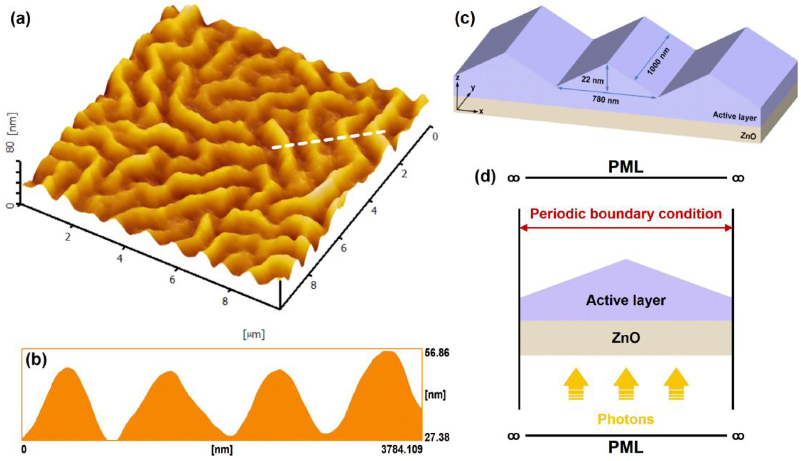
2.1. Numerical Conditions and Parameters

The simulation was performed by the FDTD algorithm [33], which is able to rigorously solve Maxwellʼs equations and makes it possible to obtain the electromagnetic field versus time and position. In the FDTD algorithm, Maxwellʼs equations are solved by a second-order approximation, the space is divided into a discrete grid, i.e., the Yee grid, and the fields are evolved in time using discrete time steps [33]. In this work, the simulation zone presented periodic conditions in the X- and Y-directions and perfectly matched layers (PML) along the Z-direction, which absorb all waves moving toward the exterior of the simulation area without reintroducing reflection [34]. The simulation mesh size was fixed at 1 nm in the Z-direction and 2 nm in the X- and Y-directions. A plane wave in normal incidence with a 200–900 nm wavelength range was used as an electromagnetic source along the Z-axis (incident from the ZnO layer). The reflectance (R) and transmittance (T) were calculated using two infinite sensors, which received all the reflected and transmitted energies, and the absorptance was derived from 1–R–T. The two sensors were considered sufficiently far from the device to avoid near-field effects [35]. The dispersion curves of the complex refractive indices of the materials are important for the accuracy of the simulation results. The real and imaginary parts of the complex refractive index, n and k, of the ZnO and PTB7-Th:PC70BM:PC60BM films were, respectively, taken from Dias [36] and Shim [37]. The ZnO film was considered a flat surface without any roughness.

2.2. Numerical Model

In the present work, we simulated the light-trapping characteristics of the SANR structures, and the establishment of equivalent numerical models with high fidelity was crucial for the credibility of the results. Therefore, we combined scanning electron microscopy (SEM, JSM-7800F, JEOL, Tokyo, Japan) and atomic force microscopy (AFM, SPA 400, Seiko instrumental, Tokyo, Japan) images for a detailed analysis of the morphology of the SANR structures. The SEM images of the SANR structures at different sizes are exhibited in Figure 1. The surface of the PTB7-Th:PC70BM:PC60BM blend film shows a large number of randomly oriented ridge-like texture structures, most of which are more than 2 µm in length, and some even more than 10 µm. In addition, the distance between adjacent textures is also random. The ridge-like texture morphology is also well-demonstrated in the AFM image (as displayed in Figure 2a), where the texture is clearly visible in the 10 µm × 10 µm area. More importantly, as revealed in Figure 2b, the cross-sectional morphology of the ridge-like texture is intact in the AFM image. The cross-section of the texture structures exhibits a ridge-like feature, and the average width and height of the ridges were 780 and 22 nm, respectively. More detailed information on the SANR structures can be found in our previously published work [32]. Based on the surface and cross-sectional morphological features of the SANR structures, we developed an equivalent numerical model, as shown in Figure 2c, where ZnO has a size of 60 nm in the Z-direction (height), and the active layer consists of a rectangle at the bottom (height 88 nm) and multiple isosceles trigonal prisms at the top (height 22 nm), with the single isosceles trigonal prism having dimensions of 780 and 1000 nm in the X- and Y-directions (width and length), respectively. The spacing between adjacent isosceles trigonal prisms is zero. The side view of the unit cell of the simulation model is displayed in Figure 2d. As a reference, we also constructed a numerical model of the flat active layer without any roughness.

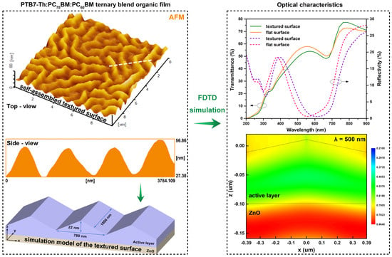
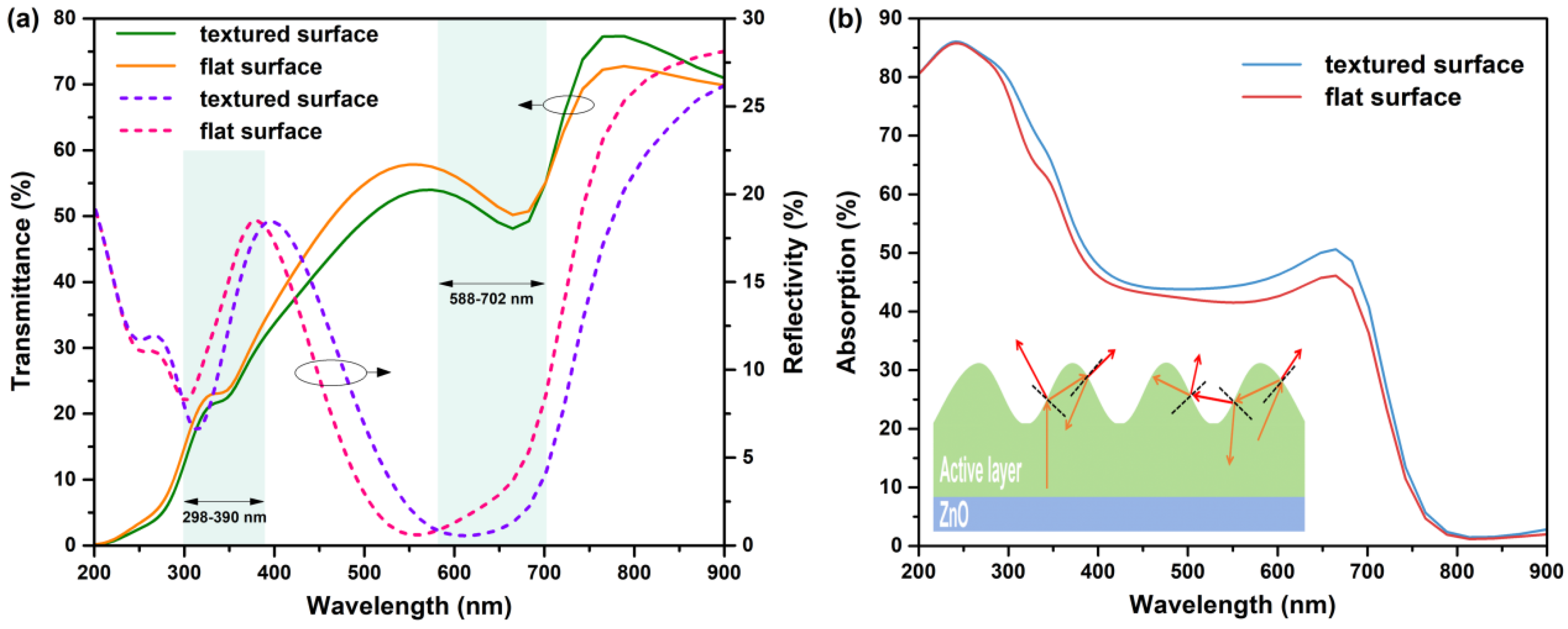
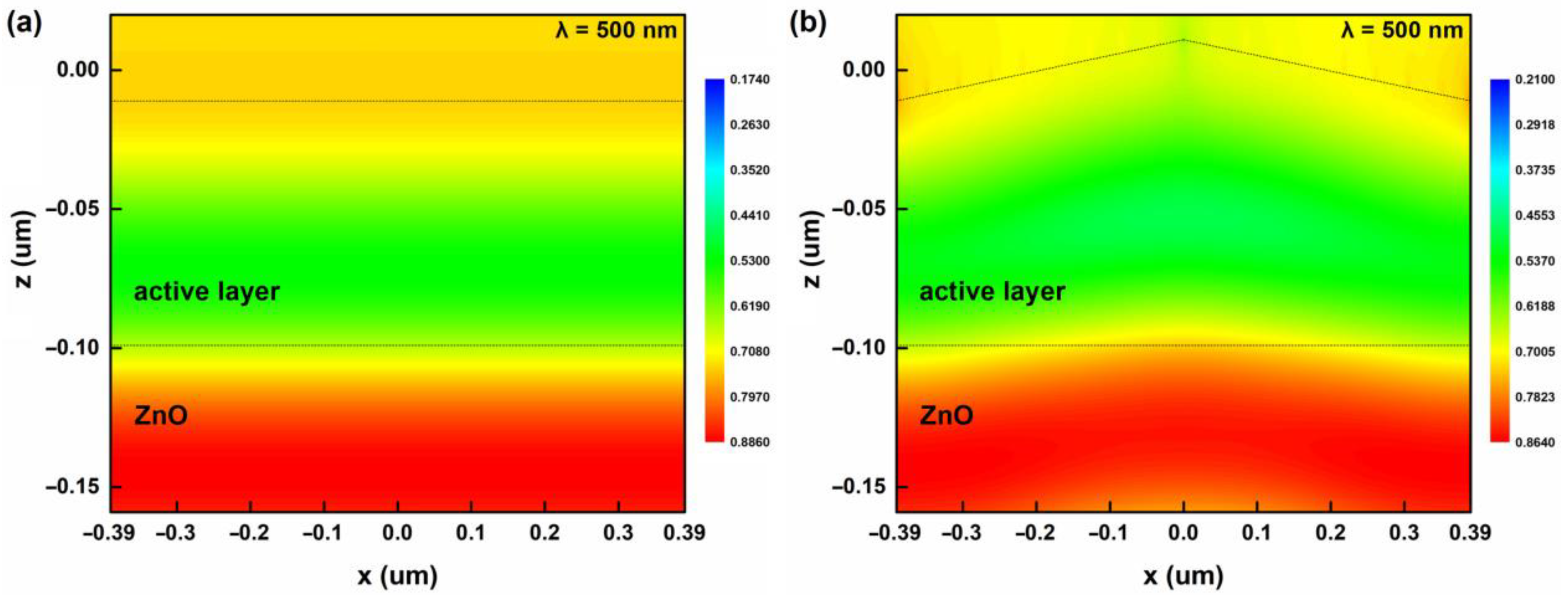
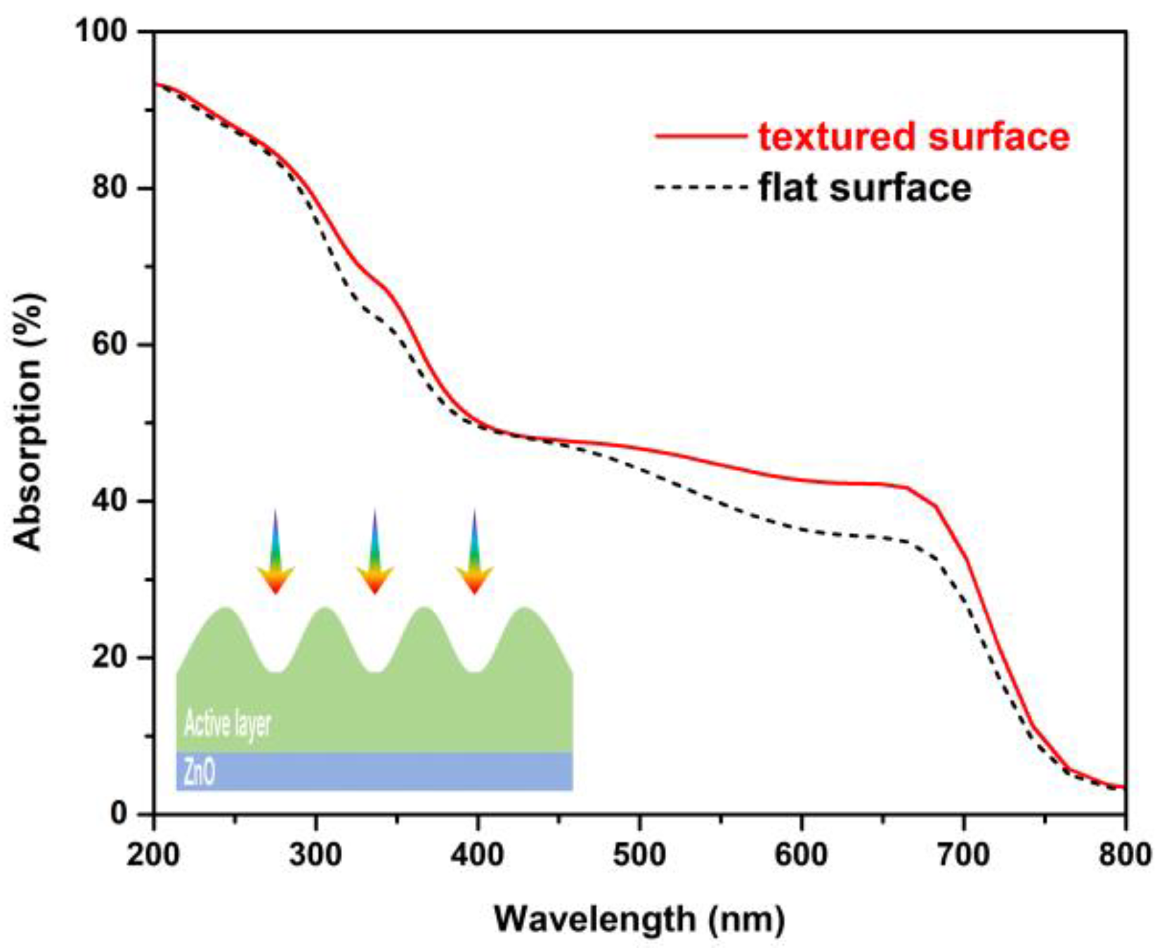
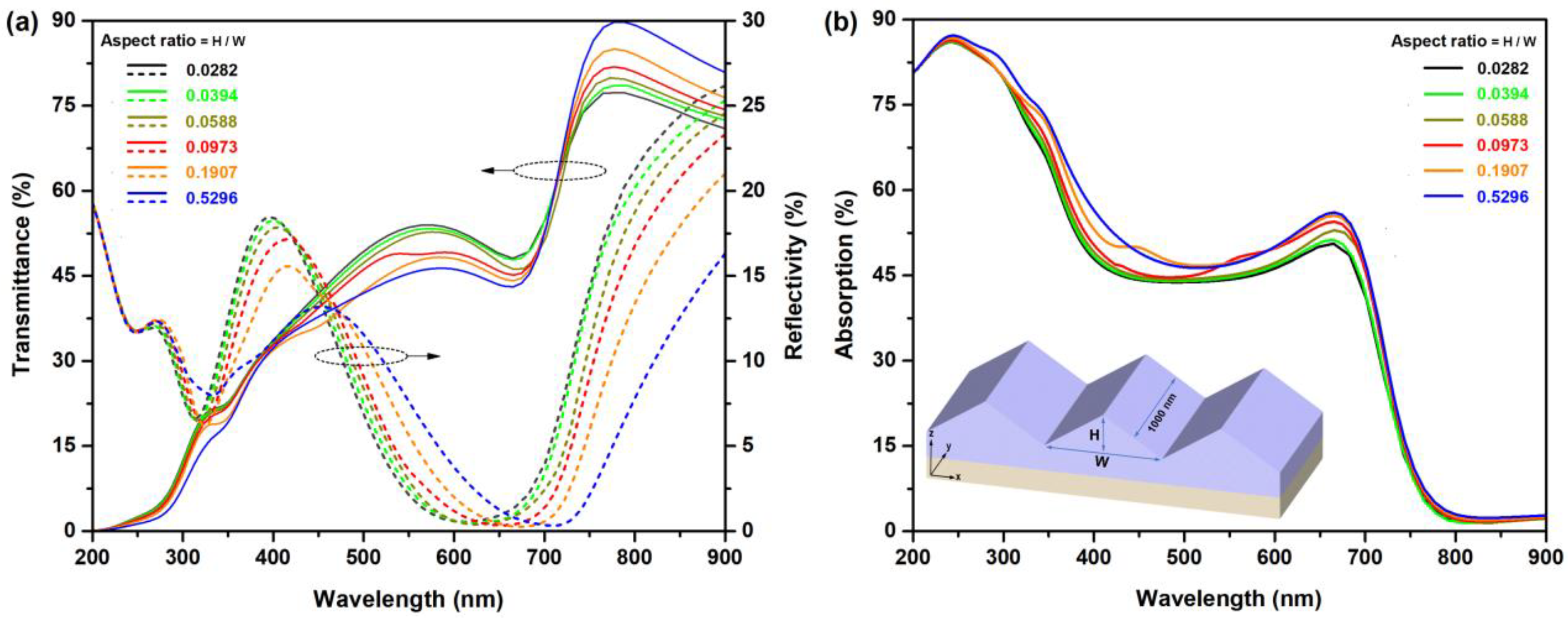
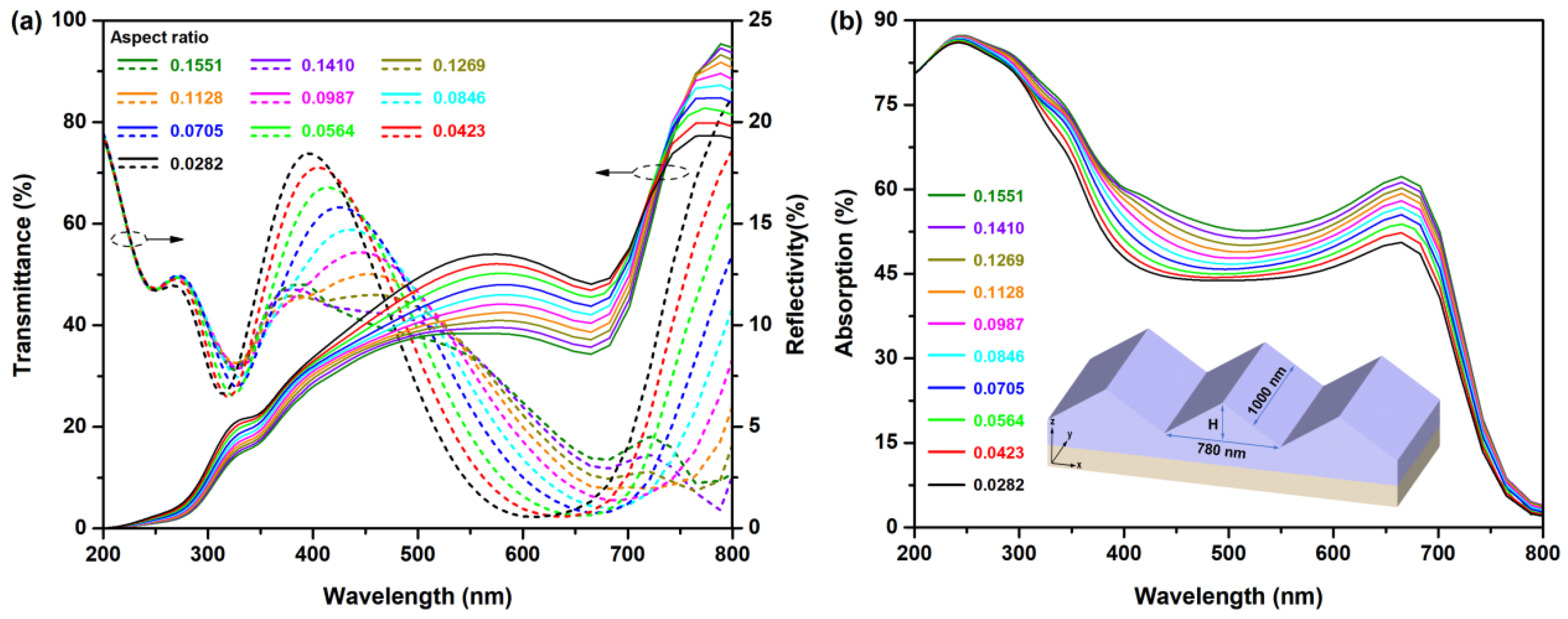
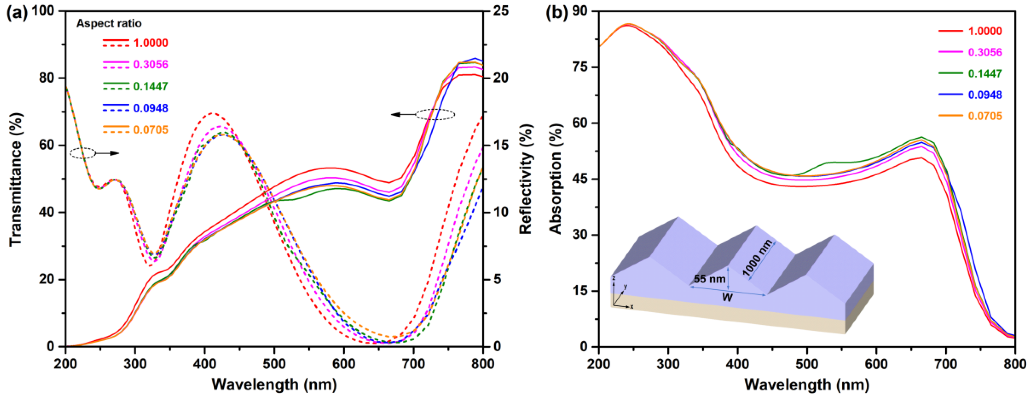
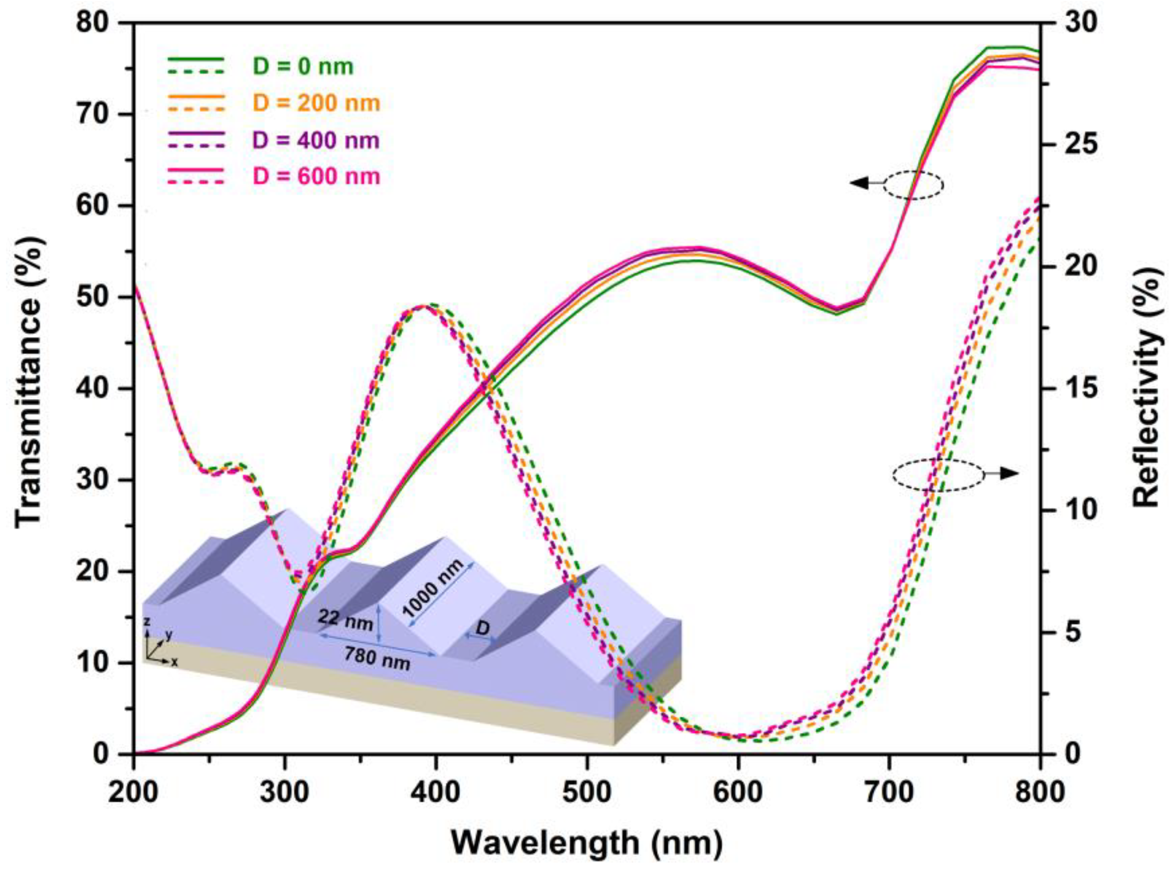
3. Results and Discussion

Our previous work provided preliminary experimental confirmation of the light-trapping effect of SANR structures, but a more comprehensive insight into their light-trapping characteristics was still necessary. It is challenging to experimentally carry out this work, so we used the FDTD algorithm to carry out prior simulation research on the light-trapping characteristics of SANR structures. The transmission and reflection spectra of the ternary blend film with SANR structures (textured surface) are shown in Figure 3a; compared with the ternary blend film without SANR structures (flat surface), the textured surface can significantly reduce the photons’ transmittance in the wavelength range of 400–600 nm and the photons’ reflectivity in the wavelength range of 600–900 nm. Although there was an increase in the photons’ transmittance and reflectance in some wavelength ranges, the overall light-trapping effect was positive. A simultaneous decrease in the photons’ transmittance and reflectance occurred in the wavelength ranges 298–390 nm and 588–702 nm, creating an effective trap for the photons. The absorption spectra obtained by 1–R–T extrapolation are listed in Figure 3b, where the photon absorption capacity of the textured surface is significantly improved, especially in the above-mentioned wavelength ranges with significant light-trapping effect. As illustrated in the inset in Figure 3b, the presence of SANR structures leads to the formation of a rough textured surface, which can increase the number of reflections and refractions of the photons at the surface, thereby increasing the optical path length of the photons in the active layer and the probability of being absorbed [38].
Figure 4 presents the cross-section images of the electric field intensity |E|2 distribution at incident wavelength of 500 nm for the blend films with flat and textured surfaces. The results illustrated that the presence of SANR structures can influence the optical field distribution of incident light within the PTB7-Th:PC70BM:PC60BM blend active layer, especially near the interface between the active layer and ZnO, and more high-energy photons are trapped near the interface, indicating that the absorption of the incident light energy is enhanced in the active layer [39]. In addition, the results revealed that the light-trapping effect of SANR structures does not depend on the direction of photon incidence. In the results in Figure 3, the photons are incident from the ZnO layer, while in the results in Figure 5, the photons are incident from the top of the active layer. It can be seen from the absorption spectra that the photon absorption of the active layer is similarly significantly enhanced, especially for the photons in the 500–700 nm wavelength range.
It is clear from the SEM and AFM images that the distribution of SANR structures has a certain randomness, and the sizes of adjacent SANR are not uniform or even very different. Therefore, it was necessary to clarify the influence of the size of the SANR structures on the light-trapping effect. Based on the established equivalent numerical model, the cross-sectional width and height were identified as the critical feature dimensions of the SANR structures. The initial feature size was 780 nm wide and 22 nm high with a cross-sectional area of 8.58 × 10³ nm2. We first kept the cross-sectional area constant and investigated the effect of changing the aspect ratio (H/W) of the numerical model on the light-trapping effect; the specific dimensional parameters are listed in Table 1. Figure 6a presents the transmission and reflection spectra of the textured surface with different aspect ratios of the SANR structures. The change in aspect ratio has a significant effect on the transmission and reflection spectra of the active layer. As the height of the SANR structures increases and the width decreases, the transmittance of the active layer to the photons in the wavelength range of 400–600 nm significantly decreases, while the transmittance to the long-wavelength (>700 nm) photons continuously increases. The reflection spectra more significantly vary with decreasing reflectance for the photons in the wavelength ranges of 320–450 nm and 700–900 nm, while with increasing reflectance for the photons in the wavelength range of 400–600 nm. The photon absorption capacity of the active layer is effectively improved by the reductions in transmittance and reflectance. With the gradual increase in the aspect ratio, the photon absorption capacity in the broad spectral wavelength range of 300–700 nm improves, as shown in Figure 6b. Reducing the width of the SANR structures corresponds to increasing the number of SANR structures per unit area (surface density), which helps to enhance the surface roughness of the active layer, and a rough surface is more conducive to light trapping [40], which is consistent with the effect of increasing the height of the SANR structures. Based on the simulation results, we inferred that in the PTB7-Th:PC70BM:PC60BM blend film with SANR structures, the size regulation of the SANR is the key to further enhancing the photon absorption capacity.
The above results clarify the dependence of the photon absorption capacity on the aspect ratio of the SANR structures, but it is obviously not enough, and we needed to further understand the effects of the independent control of the height and width of the SANR structures on the photon absorption capacity. The first focus was on the effects of height on the photon absorption capacity. We fixed the width to 780 nm and increased the height to increase the aspect ratio; the corresponding transmission and reflection spectra of the active layer are displayed in Figure 7a. With the continuous increase in the height of the SANR structures, the reflectivity to the photons with wavelengths less than 700 nm significantly decreased, especially for the photons with wavelengths in the range of 500–660 nm. When the height reached 121 nm (aspect ratio of 0.1551), compared with the height of 22 nm (aspect ratio of 0.0282), the transmittance to the photons with the wavelength of 550 nm decreased by 28.4%. Additionally, the reflectivity to the photons significantly changed, with a significant decrease for the short-wavelength photons (320–470 nm), a significant increase for the medium-wavelength photons (470–700 nm), and a significant decrease for the long-wavelength photons (>700 nm). When the height reached 121 nm, compared with the height of 22 nm, the reflectivity decreased by 36.4% and 69.0% for the photons with the wavelengths of 400 nm and 750 nm, respectively, and increased by 29.8% for the photons with the wavelength of 550 nm. The corresponding absorption spectra of the active layer are shown in Figure 7b, where the photon absorption capacity of the active layer continuously increases with the increase in the height of the SANR structures. When the height reaches 121 nm, compared with the height of 22 nm, the absorption increased by 25.0% and 20.0% for the photons with the wavelengths of 400 nm and 550 nm, respectively. Notably, the increase in height of the SANR structures is equivalent to increasing the average thickness of the active layer, which is also beneficial for improving the photon absorption capacity, and the positive effect of the increased average thickness is also shown in the results in Figure 6. Based on the simulation results, we inferred that in the PTB7-Th:PC70BM:PC60BM blend film with the SANR structures, increasing the height of the SANR structures as much as possible by regulating the process parameters will be necessary and effective to enhance the photon absorption capacity.
The effects of the width on the photon absorption capacity was our next area of interest. The above results showed that the higher the SANR, the stronger the photon absorption. However, the low stiffness of organic thin-film materials makes it more difficult to experimentally realize SANR structures with a height of 121 nm; additionally, as mentioned above, the optimal thickness of the active layer in most OSCs is around 100 nm. For this reason, it is not very reasonable to set an excessively large height of the SANR structures. Therefore, combining the characteristics of the PTB7-Th:PC70BM:PC60BM blend film with those of the SANR structures, we fixed the height at 55 nm and investigated the effects of the width on the photon absorption capacity of the active layer. The transmission, reflection, and absorption spectra of the corresponding active layer are exhibited in Figure 8. The variation in the width of the SANR has an effect on the photon transmission and reflection properties of the active layer, but the effect is much smaller than that caused by the variation in the height of the SANR structures. As revealed in Figure 8b, the reduction in the width from 780 to 180 nm does not result in a significant change in the absorption capacity of the active layer for the photons. Although the absorption spectrum of the active layer with a SANR structure width of 380 nm shows a clear absorption peak at ~530 nm, the positive effect is very limited. When the width is further reduced to 55 nm (aspect ratio of 1.0), a significant decrease in the photon absorption capacity of the active layer occurs. Combined with the results in Figure 7, the light-trapping characteristics of the PTB7-Th:PC70BM:PC60BM SANR structures are more dependent on the height of the SANR structures rather than on the width of the SANR.
Finally, attention was paid to the effects of the distance between adjacent SANR structures on the photon absorption capacity. The numerical model is illustrated in the inset in Figure 9, where the width, height, and length of the SANR structures are 780, 22, and 1000 nm, respectively. The distance between adjacent SANR structures is D, which takes the values of 0, 200, 400, and 600 nm, separately. The corresponding transmission and reflection spectra are displayed in Figure 9. Compared with the height and width of the SANR structures, the variation in the distance between adjacent SANR structures has less effect on the transmission and reflection spectra of the active layer. In general, the smaller the spacing between adjacent SANR structures, the more favorable it is to reduce the transmittance and reflectivity of the active layer for the photons in the specific wavelength ranges. When the spacing is zero, the photon absorption capacity of the active layer is optimal. Based on the simulation results, we inferred that in the PTB7-Th:PC70BM:PC60BM blend film with SANR structures, increasing the number of the SANR structures per unit area (surface density) helps to improve the photon absorption of the active layer, which is consistent with the results in Figure 6.

4. Conclusions

In this work, the light-trapping characteristics of the PTB7-Th:PC70BM:PC60BM ternary blend film with the SANR structures were investigated by using the FDTD algorithm. The results showed that the SANR structures have a light-trapping effect, which can effectively reduce the transmittance and reflectance of the incident photons at specific wavelengths and thus exhibit stronger photon absorption, especially for the photons in the wavelength range of 550–650 nm. The light-trapping effect of the SANR structures does not depend on the direction of photon incidence, and the active layer traps the photons incident from both its top and bottom. Additionally, the dimensional variation (ratio of height to width) of the SANR structures has a significant effect on the light-trapping characteristics of the active layer, and the effect caused by height variation is overwhelmingly superior compared with that of width variation. In addition, the light-trapping characteristics of the active layer is also influenced by the density of the SANR structures; the more SANR structures per unit area (i.e., the higher the surface density), the more significant the light-trapping effect of the active layer. Our work provides a basis for further experimental enhancement of the photon absorption capacity of the PTB7-Th:PC70BM:PC60BM active layer with SANR structures.

Author Contributions

Conceptualization, C.L.; methodology, C.L. and Z.Y.; software, F.L. and G.L.; validation, J.T.; formal analysis, M.C.; investigation, M.C.; resources, G.L.; data curation, C.L. and Z.Z.; writing-original draft preparation, C.L.; writing-review and editing, X.S. and J.Z.; visualization, C.L.; supervision, J.T.; project administration, X.S. and Z.Y.; funding acquisition, X.S. All authors have read and agreed to the published version of the manuscript.

Funding

This work was supported by the Hunan Provincial Natural Science Foundation of China (grant no. 2021JJ40227), the Education Department of Hunan Province (grant nos. 21B0593 and 21B0405), and the Training Program of Innovation and Entrepreneurship for Undergraduates of Hunan Province (grant no. 3726). We acknowledge the financial support of the Science and Technology Program of Hunan Province (grant no. 2019TP1014).

Institutional Review Board Statement

Not applicable.

Informed Consent Statement

Informed consent was obtained from all subjects involved in the study.

Data Availability Statement

All research results are presented in the paper, and no other supplementary materials are available.

Conflicts of Interest

The authors declare no conflict of interest.

References

  1. Zhao, C.C.; Wang, J.X.; Zhao, X.Y.; Du, Z.L.; Yang, R.Q.; Tang, J.G. Recent advances, challenges and prospects in ternary organic solar cells. Nanoscale 2021, 13, 2181–2208. [Google Scholar] [CrossRef] [PubMed]
  2. Doumon, N.Y.; Yang, L.L.; Rosei, F. Ternary organic solar cells: A review of the role of the third element. Nano Energy 2022, 94, 106915. [Google Scholar] [CrossRef]
  3. Chang, L.C.; Sheng, M.; Duan, L.P.; Uddin, A. Ternary organic solar cells based on non-fullerene acceptors: A review. Org. Electron. 2021, 90, 106063. [Google Scholar] [CrossRef]
  4. Ni, Y.F.; Liu, X.; Liu, Y.; Feng, Z.D.; Tu, D.D.; Guo, X.; Li, C. Nonalloy model-based ternary organic solar cells. ACS Appl. Mater. Interfaces 2022, 14, 12461–12468. [Google Scholar] [CrossRef]
  5. Zhu, L.; Zhang, M.; Xu, J.Q.; Li, C.; Yan, J.; Zhou, G.Q.; Zhong, W.K.; Hao, T.Y.; Song, J.L.; Xue, X.N.; et al. Single-junction organic solar cells with over 19% efficiency enabled by a refined double-fibril network morphology. Nat. Mater. 2022, 21, 656–663. [Google Scholar] [CrossRef]
  6. Sun, R.; Wu, Y.; Yang, X.; Gao, Y.; Chen, Z.; Li, K.; Qiao, J.W.; Wang, T.; Guo, J.; Liu, C.; et al. Single-junction organic solar cells with 19.17% efficiency enabled by introducing one asymmetric guest acceptor. Adv. Mater. 2022, 34, 2110147. [Google Scholar] [CrossRef]
  7. Sun, X.X.; Ni, J.; Li, C.; Huang, L.K.; Xu, R.; Li, Z.L.; Cai, H.K.; Li, J.; Zhang, J.J. Air-processed high performance ternary blend solar cell based on PTB7-Th: PCDTBT: PC70BM. Org. Electron. 2016, 37, 222–227. [Google Scholar] [CrossRef]
  8. Liu, Z.Y.; Wang, N. Small energy loss in ternary organic solar cells with a blend of cascade energy levels: Two fullerene-free acceptors as the electron acceptor. J. Mater. Chem. C 2019, 7, 10039–10048. [Google Scholar] [CrossRef]
  9. Zeng, Y.H.; Li, D.Q.; Xiao, Z.; Wu, H.B.; Chen, Z.; Hao, T.Y.; Xiong, S.B.; Ma, Z.F.; Zhu, H.M.; Ding, L.M.; et al. Exploring the charge dynamics and energy loss in ternary organic solar cells with a fill factor exceeding 80%. Adv. Energy Mater. 2021, 11, 2101338. [Google Scholar] [CrossRef]
  10. Adil, M.A.; Iqbal, M.J.; Zhang, J.; Wei, Z. Unconventional third components for ternary organic solar cells. Mater. Today Energy 2021, 21, 100728. [Google Scholar] [CrossRef]
  11. Zheng, Z.; Wang, J.Q.; Bi, P.Q.; Ren, J.Z.; Wang, Y.F.; Yang, Y.; Liu, X.Y.; Zhang, S.Q.; Hou, J.H. Tandem organic solar cell with 20.2% efficiency. Joule 2022, 6, 171–184. [Google Scholar] [CrossRef]
  12. Wang, H.T.; Zhang, Z.H.; Yu, J.S.; Liu, X.; Tang, W.H. High mobility acceptor as third component enabling high-performance large area and thick active layer ternary solar cells. Chem. Eng. J. 2021, 418, 129539. [Google Scholar] [CrossRef]
  13. Pan, F.L.; Luo, M.; Liu, X.C.; Jiang, H.Y.; Wang, Z.; Yuan, D.; Wang, Q.; Qing, L.C.; Zhang, Z.S.; Zhang, L.J.; et al. Binary non-fullerene-based polymer solar cells with a 430 nm thick active layer showing 15.39% efficiency and 73.38% fill factor. J. Mater. Chem. A 2021, 9, 7129–7136. [Google Scholar] [CrossRef]
  14. Guo, X.; Fan, Q.P.; Wu, J.N.; Li, G.W.; Peng, Z.X.; Su, W.Y.; Lin, J.; Hou, L.T.; Qin, Y.P.; Ade, H.; et al. Optimized active layer morphologies via ternary copolymerization of polymer donors for 17.6% efficiency organic solar cells with enhanced fill factor. Angew. Chem. 2021, 133, 2352–2359. [Google Scholar] [CrossRef]
  15. Yang, W.Y.; Wang, W.; Wang, Y.H.; Sun, R.; Guo, J.; Li, H.N.; Shi, M.M.; Guo, J.; Wu, Y.; Wang, T.; et al. Balancing the efficiency, stability, and cost potential for organic solar cells via a new figure of merit. Joule 2021, 5, 1209–1230. [Google Scholar] [CrossRef]
  16. Kumar, N.S.; Naidu, K.C.B. A review on perovskite solar cells (PSCs), materials and applications. J. Mater. 2021, 7, 940–956. [Google Scholar]
  17. Sobayel, M.K.; Chowdhury, M.S.; Hossain, T.; Alkhammash, H.I.; Islam, S.; Shahiduzzaman, M.; Akhtaruzzaman, M.; Techato, K.; Rashid, M.J. Efficiency enhancement of CIGS solar cell by cubic silicon carbide as prospective buffer layer. Sol. Energy 2021, 224, 271–278. [Google Scholar] [CrossRef]
  18. Shuai, Z.G.; Wang, L.J.; Li, Q.K. Evaluation of charge mobility in organic materials: From localized to delocalized descriptions at a first-principles level. Adv. Mater. 2011, 23, 1145–1153. [Google Scholar] [CrossRef]
  19. Lin, Y.B.; Nugraha, M.I.; Firdaus, Y.; Scaccabarozzi, A.D.; Aniés, F.; Emwas, A.H.; Yengel, E.; Zheng, X.P.; Liu, J.K.; Wahyudi, W.; et al. A simple n-dopant derived from diquat boosts the efficiency of organic solar cells to 18.3%. ACS Energy Lett. 2020, 5, 3663–3671. [Google Scholar] [CrossRef]
  20. Zhao, C.C.; Wang, J.X.; Jiao, J.Q.; Huang, L.J.; Tang, J. Recent advances of polymer acceptors for high-performance organic solar cells. J. Mater. Chem. C 2020, 8, 28–43. [Google Scholar] [CrossRef]
  21. Tong, Y.; Xiao, Z.; Du, X.Y.; Zuo, C.T.; Li, Y.L.; Lv, M.L.; Yuan, Y.B.; Yi, C.Y.; Hao, F.; Hua, Y.; et al. Progress of the key materials for organic solar cells. Sci. China Chem. 2020, 63, 758–765. [Google Scholar] [CrossRef]
  22. Wang, L.J.; Nan, G.J.; Yang, X.D.; Peng, Q.; Li, Q.K.; Shuai, Z.G. Computational methods for design of organic materials with high charge mobility. Chem. Soc. Rev. 2010, 39, 423–434. [Google Scholar] [CrossRef]
  23. Wang, Y.F.; Liang, Z.Z.; Li, X.M.; Qin, J.C.; Ren, M.L.; Yang, C.Y.; Bao, X.C.; Xia, Y.J.; Li, J.F. Self-doping n-type polymer as a cathode interface layer enables efficient organic solar cells by increasing built-in electric field and boosting interface contact. J. Mater. Chem. C 2019, 7, 11152–11159. [Google Scholar] [CrossRef]
  24. Gao, W.; An, Q.S.; Hao, M.H.; Sun, R.; Yuan, J.; Zhang, F.J.; Ma, W.; Min, J.; Yang, C.L. Thick-film organic solar cells achieving over 11% efficiency and nearly 70% fill factor at thickness over 400 nm. Adv. Funct. Mater. 2020, 30, 1908336. [Google Scholar] [CrossRef]
  25. Kang, D.J.; Kang, H.; Cho, C.; Kim, K.H.; Jeong, S.; Lee, J.Y.; Kim, B.J. Efficient light trapping in inverted polymer solar cells by a randomly nanostructured electrode using monodispersed polymer nanoparticles. Nanoscale 2013, 5, 1858–1863. [Google Scholar] [CrossRef]
  26. Chen, J.Y.; Yu, M.H.; Chang, C.Y.; Chao, Y.H.; Sun, K.W.; Hsu, C.S. Enhanced performance of organic thin film solar cells using electrodes with nanoimprinted light-diffraction and light-diffusion structures. ACS Appl. Mater. Interfaces 2014, 6, 6164–6169. [Google Scholar] [CrossRef]
  27. Na, S.I.; Kim, S.S.; Jo, J.; Oh, S.H.; Kim, J.; Kim, D.Y. Efficient polymer solar cells with surface relief gratings fabricated by simple soft lithography. Adv. Funct. Mater. 2008, 18, 3956–3963. [Google Scholar] [CrossRef]
  28. Qiao, L.F.; Wang, D.; Zuo, L.J.; Ye, Y.Q.; Qian, J.; Chen, H.Z.; He, S.L. Localized surface plasmon resonance enhanced organic solar cell with gold nanospheres. Appl. Energy 2011, 88, 848–852. [Google Scholar] [CrossRef]
  29. Wu, J.L.; Chen, F.C.; Hsiao, Y.S.; Chien, F.C.; Chen, P.; Kuo, C.H.; Huang, M.H.; Hsu, C.S. Surface plasmonic effects of metallic nanoparticles on the performance of polymer bulk heterojunction solar cells. ACS Nano 2011, 5, 959–967. [Google Scholar] [CrossRef]
  30. Pastorelli, F.; Romero-Gomez, P.; Betancur, R.; Martinez-Otero, A.; Mantilla-Perez, P.; Bonod, N.; Martorell, J. Enhanced light harvesting in semitransparent organic solar cells using an optical metal cavity configuration. Adv. Energy Mater. 2015, 5, 1400614. [Google Scholar] [CrossRef]
  31. Yang, Y.; Mielczarek, K.; Aryal, M.; Zakhidov, A.; Hu, W. Nanoimprinted polymer solar cell. ACS Nano 2012, 6, 2877–2892. [Google Scholar] [CrossRef]
  32. Li, C.; Tao, J.Y.; Zou, Z.J.; Liao, G.H.; Li, F.; Wang, J.F.; Sun, X.X.; Ni, J.; Zhang, J.J. Broad spectrum light-trapping ternary polymer solar cells based on self-assembled nano-ridged active layer. Sol. Energy 2020, 198, 1–7. [Google Scholar] [CrossRef]
  33. Oskooi, A.F.; Roundy, D.; Ibanescu, M.; Bermel, P.; Joannopoulos, J.D.; Johnson, S.G. MEEP: A flexible free-software package for electromagnetic simulations by the FDTD method. Comput. Phys. Commun. 2010, 181, 687–702. [Google Scholar] [CrossRef]
  34. Vedraine, S.; Torchio, P.; Duché, D.; Flory, F.; Simon, J.J.; Le Rouzo, J.; Escoubas, L. Intrinsic absorption of plasmonic structures for organic solar cells. Sol. Energy Mater. Sol. Cells 2011, 95, S57–S64. [Google Scholar] [CrossRef]
  35. Duche, D.; Torchio, P.; Escoubas, L.; Monestier, F.; Simon, J.J.; Flory, F.; Mathian, G. Improving light absorption in organic solar cells by plasmonic contribution. Sol. Energy Mater. Sol. Cells 2009, 93, 1377–1382. [Google Scholar] [CrossRef]
  36. Aguilar, O.; de Castro, S.; Godoy, M.P.F.; Dias, M.R.S. Optoelectronic characterization of Zn1-xCdxO thin films as an alternative to photonic crystals in organic solar cells. Opt. Mater. Express 2019, 9, 3638–3648. [Google Scholar] [CrossRef]
  37. Shin, S.C.; Vincent, P.; Bae, J.H.; Lee, J.J.; Nam, M.; Ko, D.H.; Kim, H.; Shim, J.W. Quaternary indoor organic photovoltaic device demonstrating panchromatic absorption and power conversion efficiency of 10%. Dye. Pigment. 2019, 163, 48–54. [Google Scholar] [CrossRef]
  38. Chen, P.Z.; Hou, G.F.; Fan, Q.H.; Ni, J.; Zhang, J.J.; Huang, Q.; Zhang, X.D.; Zhao, Y. Combining randomly textured surfaces and one-dimensional photonic crystals as efficient light-trapping structures in hydrogenated amorphous silicon solar cells. Sol. Energy Mater. Sol. Cells 2015, 143, 435–441. [Google Scholar] [CrossRef]
  39. Chen, J.D.; Cui, C.H.; Li, Y.Q.; Zhou, L.; Ou, Q.D.; Li, C.; Li, Y.F.; Tang, J.X. Single-junction polymer solar cells exceeding 10% power conversion efficiency. Adv. Mater. 2015, 27, 1035–1041. [Google Scholar] [CrossRef]
  40. Palanchoke, U.; Jovanov, V.; Kurz, H.; Dewan, R.; Magnus, P.; Stiebig, H.; Knipp, D. Influence of back contact roughness on light trapping and plasmonic losses of randomly textured amorphous silicon thin film solar cells. Appl. Phys. Lett. 2013, 102, 083501. [Google Scholar] [CrossRef]
Figure 1. SEM images of the PTB7-Th:PC70BM:PC60BM blend film with SANR structures under different scales: (a) 2 μm, (b) 1 μm, and (c) 200 nm.
Coatings 12 01340 g001
Figure 2. (a) Top view and (b) side view of the AFM images of the PTB7-Th:PC70BM:PC60BM blend film with SANR structures, (c) schematic diagram of the numerical model, and (d) side view of the unit cell of the simulation model.
Coatings 12 01340 g002
Figure 3. (a) Transmission and reflection spectra of the blend films with textured and flat surface and (b) corresponding absorption spectra. The inset shows the light-trapping mechanism of the textured surface.
Coatings 12 01340 g003
Figure 4. The normalized cross-section near-field profiles of TM-polarized light for normal-incidence monochromatic illumination at the wavelength of 500 nm in the blend films with (a) flat and (b) textured surfaces.
Coatings 12 01340 g004
Figure 5. Absorption spectra of the blend films with textured and flat surfaces. The photons are incident from the top of the active layer as demonstrated in the inset.
Coatings 12 01340 g005
Figure 6. (a) Transmission and reflection spectra of the textured surface with different aspect ratios of the SANR structures and (b) corresponding absorption spectra. The inset demonstrates the structural parameters of the numerical model; the specific values are listed in Table 1.
Coatings 12 01340 g006
Figure 7. (a) Transmission and reflection spectra of the textured surface with different aspect ratios of the SANR structures and (b) corresponding absorption spectra. The inset demonstrates the structural parameters of the numerical model: the width was fixed at 780 nm and the height was changed, thus changing the aspect ratio.
Coatings 12 01340 g007
Figure 8. (a) Transmission and reflection spectra of the textured surface with different aspect ratios of the SANR structures and (b) corresponding absorption spectra. The inset demonstrates the structural parameters of the numerical model; the height was fixed at 55 nm and the width was changed, thus changing the aspect ratio.
Coatings 12 01340 g008
Figure 9. Transmission and reflection spectra of the textured surface with different spacings between adjacent SANR structures. The inset demonstrates the structural parameters of the numerical model: the width, height, and length of each ridge were fixed at 780, 22, and 1000 nm, respectively.
Coatings 12 01340 g009
Table 1. Specific parameters for the equivalent SANR structures with different aspect ratios.
Height (nm)Width (nm)Aspect Ratio (H/W)
22 7800.0282
266600.0394
31.8 5400.0588
40.9 4200.0973
57.2 3000.1907
95.3 1800.5296
Publisher’s Note: MDPI stays neutral with regard to jurisdictional claims in published maps and institutional affiliations.

