Article

On the Control of Hot Nickel Target Magnetron Sputtering by Distribution of Power Pulses

by
Rafal Chodun
1,*,
Bartosz Wicher
1,
Katarzyna Nowakowska-Langier
2,
Roman Minikayev
3,
Marlena Dypa-Uminska
1 and
Krzysztof Zdunek
1
1
Faculty of Materials Science and Engineering, Warsaw University of Technology, Woloska 141, 02-507 Warsaw, Poland
2
National Centre for Nuclear Research, Andrzeja Soltana 7, 05-400 Otwock-Swierk, Poland
3
Institute of Physics of the Polish Academy of Sciences, al. Lotnikow 32/46, 02-668 Warsaw, Poland
*
Author to whom correspondence should be addressed.
Coatings 2022, 12(7), 1022; https://doi.org/10.3390/coatings12071022
Submission received: 1 July 2022 / Revised: 11 July 2022 / Accepted: 16 July 2022 / Published: 19 July 2022
(This article belongs to the Special Issue Advances in Thin Film Fabrication by Magnetron Sputtering)

Abstract

:
This paper presents the experimental results of high-temperature sputtering of nickel targets by the Gas Injection Magnetron Sputtering (GIMS) technique. The GIMS technique is a pulsed magnetron sputtering technique that involves the generation of plasma pulses by injecting small doses of gas into the zone of the magnetron target surface. Using a target with a dedicated construction to limit heat dissipation and the proper use of injection parameters and electrical power density, the temperature of the target during sputtering can be precisely controlled. This feature of the GIMS technique was used in an experiment with sputtering nickel targets of varying thicknesses and temperatures. Plasma emission spectra and current-voltage waveforms were studied to characterize the plasma process. The thickness, structure, phase composition, and crystallite size of the nickel layers produced on silicon substrates were investigated. Our experiment showed that although the most significant increase in growth kinetics was observed for high temperatures, the low sputtering temperature range may be the most interesting from a practical perspective. The excited plasma has the highest energy in the sputtering temperature range, just above the Curie temperature.

1. Introduction

One branch of magnetron sputtering technology has attracted strong interest recently. This branch is the so-called Hot Target Magnetron Sputtering (HTMS) technique [1,2]. HTMS aims to run a cathode sputtering process with an increased temperature. It is possible by modifying the construction of the magnetron target and involves the creation of a break in the contact area with the cooled surface. The flux of dissipated heat is reduced, and the target itself accumulates a significant heat load in its volume, raising its temperature. The primary purpose of this procedure is to increase the target material’s vapor pressure and lead to its sublimation. The stream of particles produced during such a process of sputtering and reaching the substrate is significantly enriched by the stream of sublimated species. Densified plasma flux is reflected in a considerable increase in the growth kinetics of the coatings and leads to a significant economization of the technological process [3]. One of the varieties of HTMS processes is the intentional increase in target temperature above the melting point of Liquid Target Magnetron Sputtering [4]. This way, the species flux reaching the substrate is enriched with evaporated particles. The kinetics of growth is one of the critical parameters determining the applicability of the magnetron sputtering technique and seems to be of particular importance in its variants where low growth kinetics is a genetic feature of the technique. This group of methods includes pulsed methods such as High Power Magnetron Sputtering (HiPIMS). A variation in HTMS has also found positive effects in HiPIMS technology [5,6,7,8,9].
One practical purpose of using HTMS is to sputter target ferromagnetic materials effectively. Sputtering of magnetic materials is highly difficult in standard magnetron sputtering techniques as ferromagnetic materials confine magnetic field lines within their volume. The magnetic field strength above the surface of the target is attenuated, resulting in difficulty initiating and sustaining a glow discharge [10]. Magnetron sputtering technology employs various approaches to overcome these obstacles, such as using additional sources of plasma excitation [11,12,13], thin targets [14], and particular magnetic field configuration [15,16]. Although the mentioned methods have undoubted advantages, they are not ideal, and new solutions are still being sought. One of the more exciting and newer ideas is the HTMS technique to conduct the sputtering process at the target temperature above the Curie temperature TC. This way, sputtering of ferromagnetic materials is efficient. The HTMS technique has already been used to sputter nickel targets [17,18]. So far, the authors are not aware of any published work showing the application of HTMS in the cases of iron and cobalt. This is due to the shielding effect of the magnetic field and the difficulty in controlling the temperature. These metals have much higher TC than nickel, 770 and 1121 °C, respectively. The magnitude of the difficulty is mainly indicated by the approach of the TC to the melting point; in these cases, they are, respectively: 1538 and 1495 °C. “Temperature window” of sputtering processes is thus narrower and at a higher temperature. The most promising development track of the HTMS technique is the effective control of the target temperature.
Target temperature control is a critical issue in HTMS technology. Without it, the magnetron target can be plastically deformed due to creeping or whole magnetron construction can be seriously damaged. The permanent magnet system is particularly vulnerable. Another risk is the possibility of melting the target material. Another factor to consider is the effect of heat radiation on the plasma and the substrate–growing coating system. These issues have not yet been widely discussed in the literature, and the reason can be speculated to be the difficulty in achieving arbitrary sputtering temperature determination. The factor that is standardly used to establish the temperature of the target, the electrical power density, is probably insufficient in HTMS technological practice. Recently, our team has used Gas Injection Magnetron Sputtering (GIMS) for HTMS technology [19]. At that stage, we thought that by using GIMS, we would introduce a crucial temperature control parameter. The GIMS technique is a pulsed technique that uses the generation of discrete plasma streams (plasma pulses) in an environment of dynamically varying working gas concentration, controlled by high-speed pulsed gas valves [20,21]. Typically, in GIMS, layers are produced due to the generation of 10–102 ms plasma pulses at frequencies of 10−1–101 s. The pulse power density is of the order of 102 W/cm2. Controlling the pulsing parameter, i.e., frequency and single pulse lifetime, allowed us to set the sputtering temperature reasonably precisely.
In this experiment, we aimed to exploit the advantages of using the GIMS technique in HTMS technology and see if it is effective in sputtering nickel targets. The second objective of our experiment was to characterize the HTMS process of nickel targets with varying thicknesses (magnetic field shielding strength) at various temperatures.

2. Materials and Methods
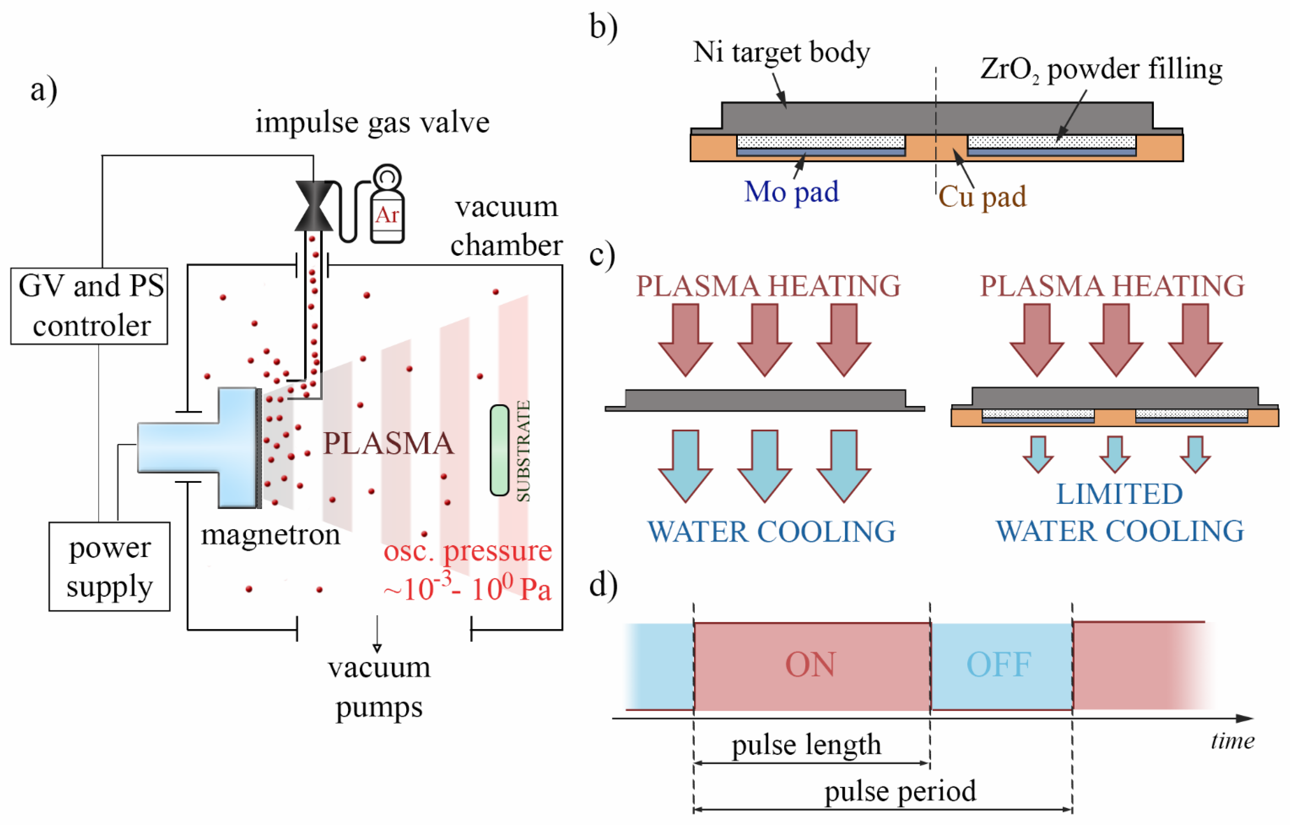
2.1. Apparatus

HTMS processes were carried out in a vacuum apparatus presented in Figure 1a. The vacuum chamber was equipped with a vacuum pump system consisting of turbomolecular, roots, and rotary pumps. The vacuum pump unit could reach a base pressure of 5 × 10⁻³ Pa. An extremely unbalanced, according to Gencoa criterion [22], circular magnetron was used as the plasma source. The 50 mm diameter nickel targets (Grade 1 purity) were installed in the magnetron.
Figure 1b presents the sandwich construction of the used targets. The target sandwich consisted of a nickel target, ZrO2 powder filling, molybdenum foil, and a copper pad. The 1.5, 2, 2.5, and 3 mm thick nickel targets were used for the experiment. A 1.5-mm deep channel was fabricated in the copper pad. The channel was filled with ZrO2 powder to provide low thermal conductivity at the high-temperature zone of the target system. Additionally, a zirconia filling prevented material deformation due to high temperature. During the coating deposition, the bottom surface of the copper pad was cooled with water. The qualitative difference between hot and standard sputtering is presented in Figure 1c.

2.2. Coatings Deposition Process

Coating deposition processes were carried out using argon as sputtering gas (N5.0 purity). The working atmosphere was created by injections from a fast pulse valve directly at the target surface. The pressure at the valve inlet was set at 1.5 × 10⁵ Pa. The opening time of the Ar valve was fixed at 4 ms. The applied gas settings resulted in a pressure oscillation with a peak of about 10−1 Pa. A precise determination of the oscillation was impossible due to the high time inertia of the used vacuum gauge. Pawlak in [23] studied a more accurate study of the pressure characteristic in GIMS.
The plasma 500 ms pulse length and period were the parameters controlling the target temperature in the experiment. Individual power pulses are electronically coupled to the opening moment of the pulsed gas valve. The electronic coupling of the power supply to the valve operation allows the precise determination of the glow discharge at a fixed time from the gas injection. In this experiment, we established the discharge when opening the valve and sustaining it for 500 ms. The interaction of plasma energetic species with the target surface induces thermal energy in the target material. The energy distribution has a pulsed manner in GIMS. Therefore, relatively frequent events of thermal excitation (plasma pulses) increase the temperature of the target material. During the interval between pulses, the accumulated heat is partially dissipated. The heat dissipation is effective when the impulse interval is longer [19]. The pulse length and pulse periods are described in detail in Table 1 with the other process parameters. Figure 1d schematically presents the power pulses time distribution in the GIMS process. The nature of the thermal excitation was pulsed, and the target was continuously heated up during the plasma phase until a specific target temperature resulting from the system’s ability to dissipate heat was established. Each discharge is followed by the period of the dissipation of the accumulated heat. The temperature characteristics during the process of sputtering can be considered quasi-stationary. The temperature of the targets was measured using an MM2MH Raytek pyrometer and high-speed Optris Xi400 thermal camera. The center of the target was the spot with the highest temperature. The temperature data in Table 1 shows the pyrometer measurement results at the target’s center. As the sensitivity of the pyrometer starts at 450 °C, the process labeled “<450” in the table was performed at low-temperature conditions, below the TC.
The n-type 100 silicon substrates were prepared by ultrasonic cleaning in acetone and drying. After that, they were located perpendicularly to the magnetron Z-axis at 10 cm from its surface. The substrate stage was electrically grounded during coating deposition with the magnetron anode and vacuum chamber. The magnetron system was powered using a Dora Power Systems pulsed DC power supply with a carrier frequency of 125 kHz [24,25].
The power waveforms were calculated from the current and voltage characteristics, measured using the 1 A: 0.1 V Rogowski coil and 1 kV: 1 V voltage, and registered by a Rigol oscilloscope. The pulse energy was calculated using the integral over time. All the calculations were made using the Origin Lab software. The distribution of normal magnetic field B at the surface of the nickel targets used in the experiments was investigated by SMS-102 Asonik Hall effect meter.

2.3. Plasma Characterization

The optical emission spectroscopy (OES) measurements were obtained using an Optel energy-dispersive optical spectrometer at a wavelength of 200–900 nm. The signals were collected through a quartz window and an optical fiber. The exposition time was set at a full single plasma pulse. During these experiments, the optical collimator was perpendicular to the magnetron Z-axis and placed 55 mm away from the cathode surface.

2.4. Coatings Characterization

The deposited coatings were further characterized by scanning electron microscopy (SEM). The cross-section of nickel coatings fabricated at silicon substrates was observed at a 45° to the surface plane using a ZEISS Ultra Plus device. The cross-sections of the samples were obtained by brittle fracture just after cooling them in liquid nitrogen.
The crystal structure of the coatings was analyzed by X-ray diffraction (XRD) using Cu-Kα radiation. The XRD profiles of the layers were measured at a 2θ range of 15–120°. The Debye–Scherrer equation was used to calculate the size of crystallites. Crystalline size D , is expressed:
D = K λ β cos θ
where D is the size of the grain, K is known as the Scherer’s constant (K = ~0.9), λ is the X-ray wavelength (for Cu 1.54178Å), β is full width at half maximum (FWHM) of the diffraction peak, and θ is the angle of diffraction.

3. Results and Discussion

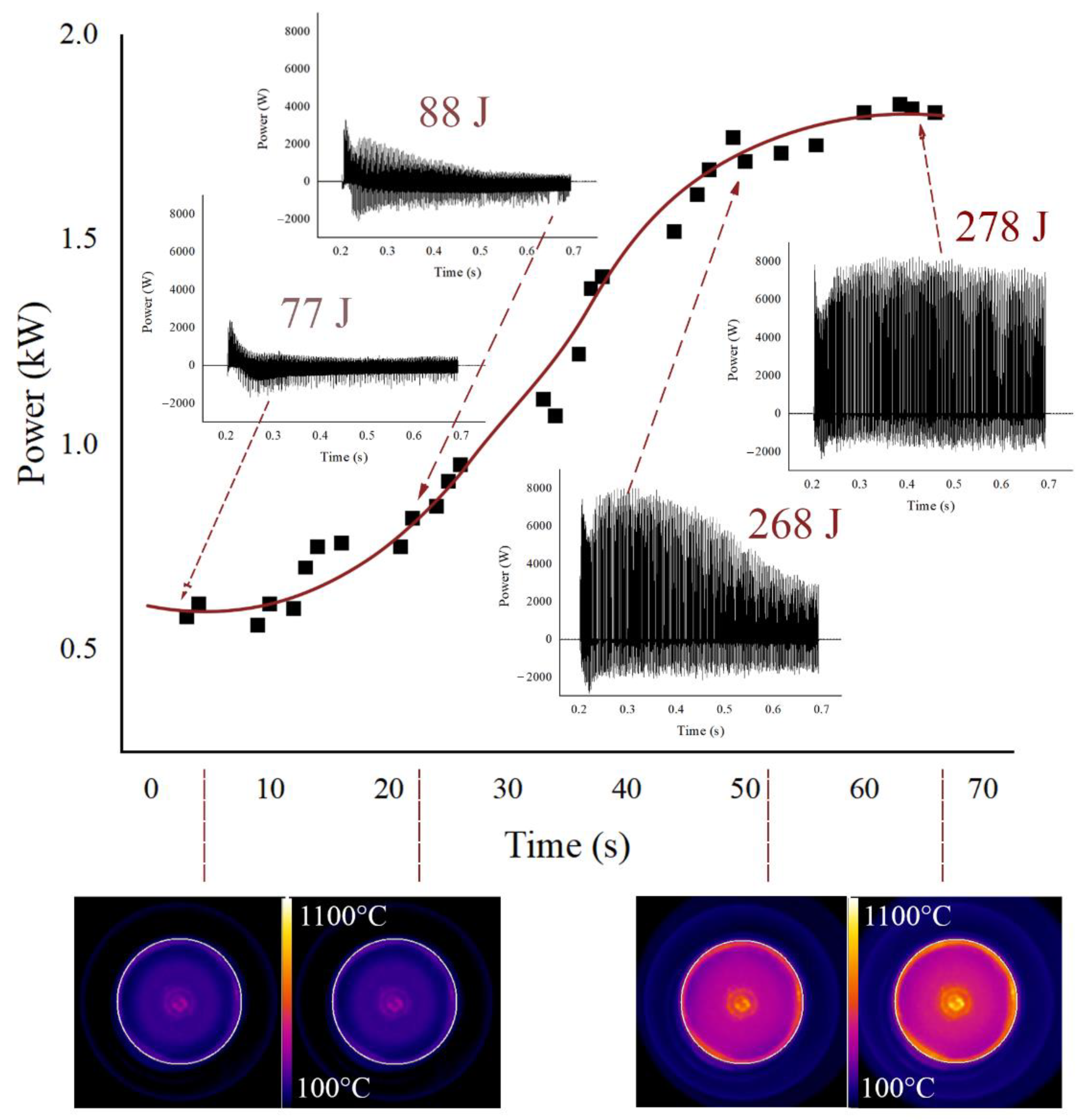
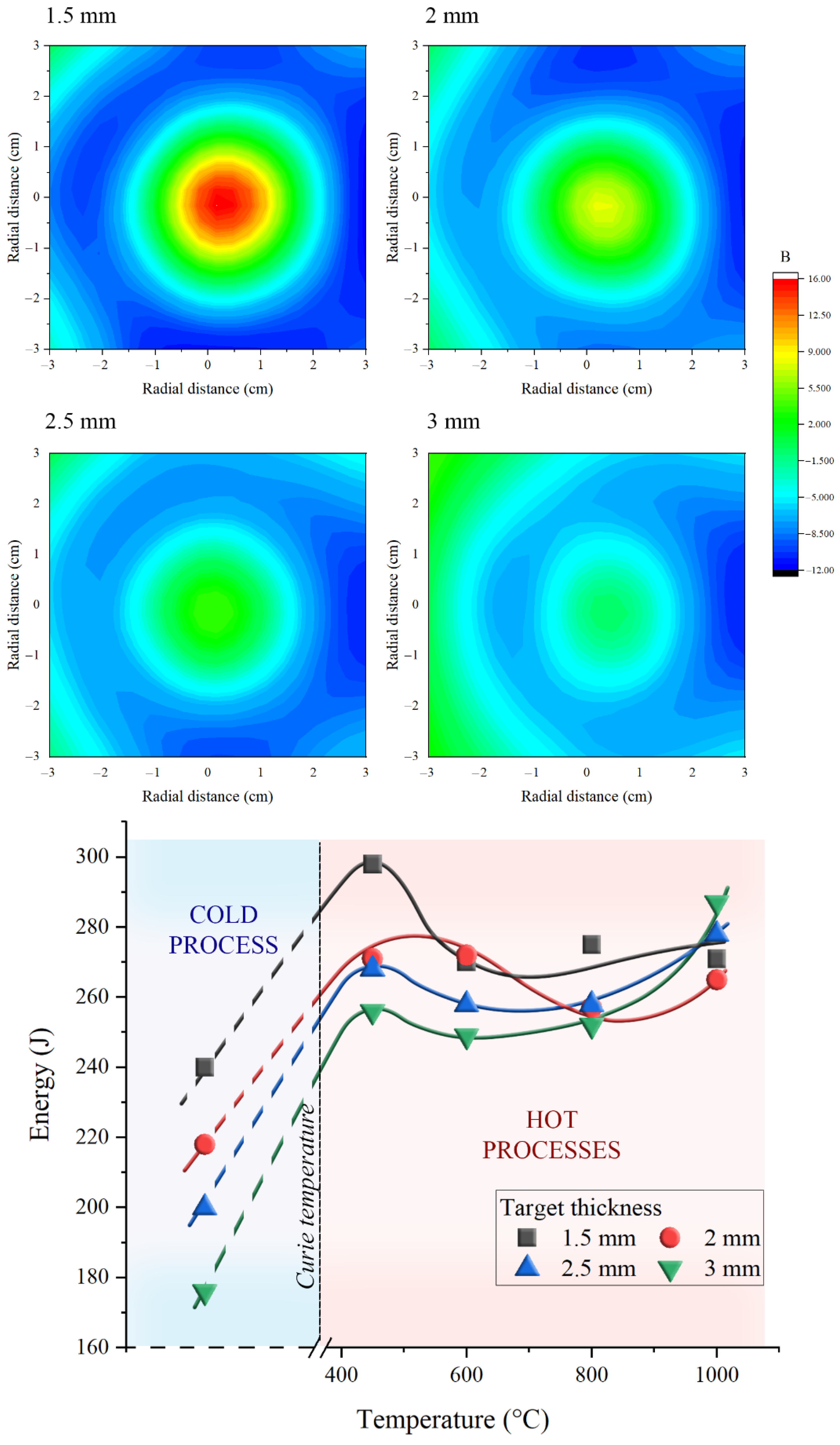
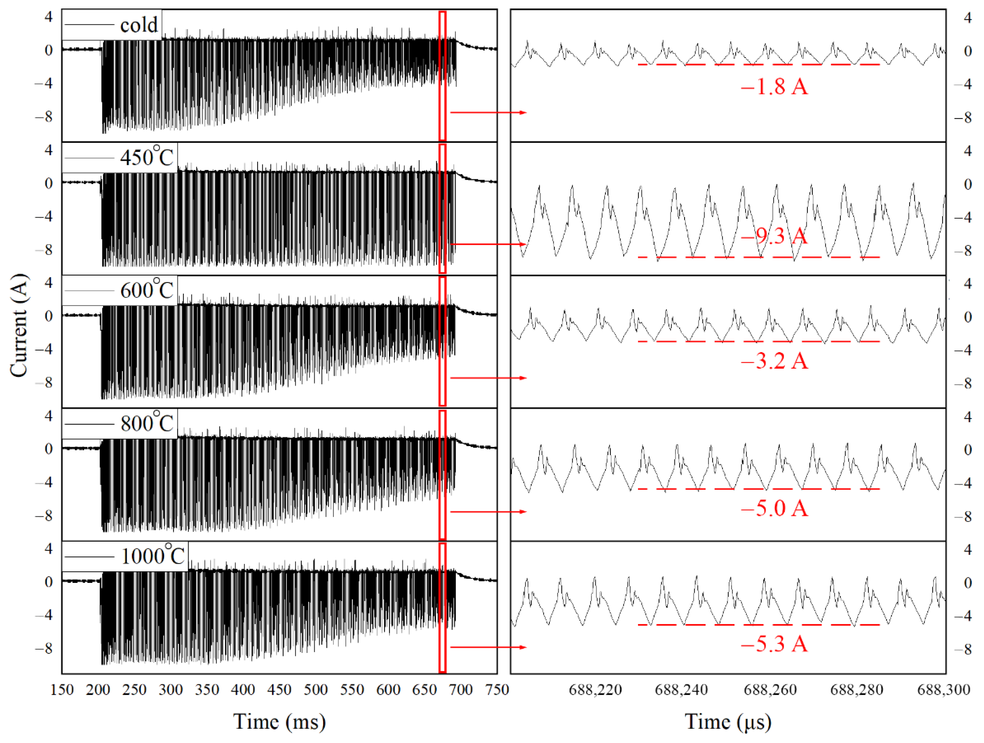
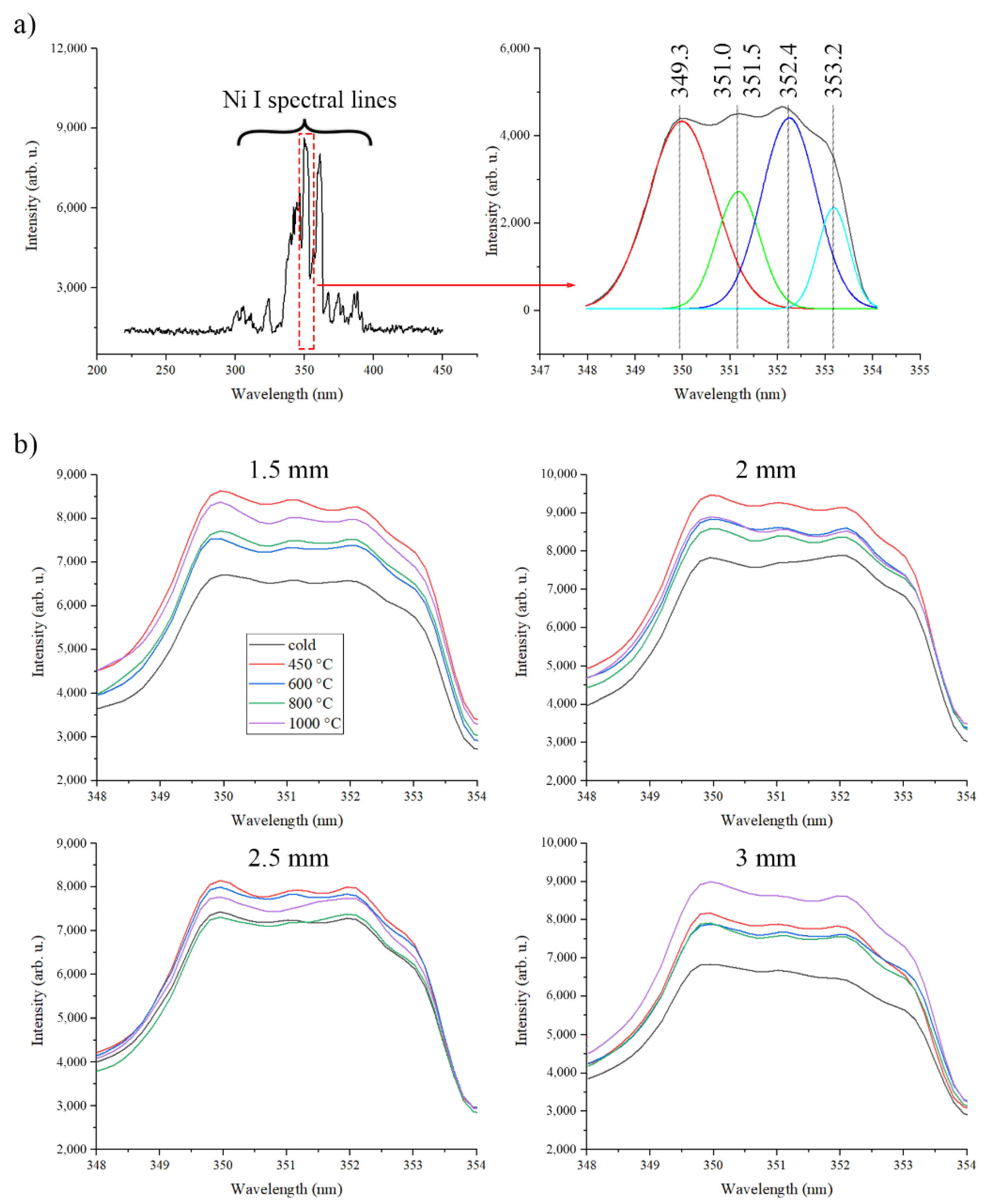
3.1. Plasma Characterization

The first step in the experiment was to characterize the sputtering process of the nickel target during its progressive heating. For this purpose, current and voltage waveforms were measured at distinct stages of heating a nickel target 1.5 mm thick. Power waveforms were determined based on the indications of the electric power supply integrating the current and voltage waveforms in situ during its operation. The results are shown in Figure 2. The figure shows the fitting of the discharge power curve during the heating of the target. At the initial stage, when the target material’s volume is below the Curie temperature, the glow discharge is characterized by relatively low power. The power increases when an increased volume of the target material exhibits a transition from a ferromagnetic state to a non-magnetic state. The nature of the transition is relatively smooth and is associated with a gradual increase in the volume of the non-magnetic fraction of the nickel target. In the final part of the curve, the power value stabilizes. Power stabilization is associated with forming a constant volume of non-magnetic material of the target. Images taken with a thermal camera at distinct stages of heating the target are attached to the figure. When considering the temperature of the target in the HTMS process, it is necessary to keep in mind its irregular distribution in the volume. The images clearly show that its hottest parts are primarily in the center. As the sputtering temperature increases, the pulse power waveforms also change significantly. The figure presents examples of the curve’s power waveforms measured in characteristic parts. The power pulses were integrated, and the energy of a single pulse was determined—also shown in the figure. The nature of the changes in the energy values is related to the amplitude of the power waveform, which is the result of changes in the discharge current waveform.
The next stage of our experiment was to study the effect of temperature and thickness of the nickel target on the energy of the glow discharge. Sputtering processes of nickel targets were carried out in the temperature range up to 1000 °C. The temperature was controlled by adjusting the period of triggering the plasma pulse according to Table 1. Targets with thicknesses of 1.5, 2, 2.5, and 3 mm were sputtered. Using targets of different thicknesses, we could characterize the discharge under various magnetic field energy supports. The effect of target thickness on B is shown in Figure 3. The magnetron used in the initial state has a maximum intensity of 90 mT. Using a cathode system with a 1.5 mm nickel target reduced the B maximum to ~16 mT. B of ~1.5 mT characterized the 3 mm target. The magnetic field intensity distribution over the target itself does not change much. Figure 3 also shows the energy characteristics as a function of sputtering temperature. The thickness of the target, that is, the B value, significantly affects the pulse energy. The characteristics themselves are interesting. In the range of temperatures, in which we conducted measurements, the maximum energy was noted at temperatures ~100 °C above TC. In the range of about 500–900 °C, we observed a decrease in the pulse’s energy. At temperatures above 900 °C, the energy value increased again.
The parameter controlling the pulse energy value is the character of the power waveform, which in turn is determined by the discharge current characteristics. Figure 4 shows the discharge current waveforms measured while sputtering a 1.5 mm nickel target at different temperatures. Temperatures at which the pulse energy was relatively low are characterized by current decay at the end of the discharge duration.
The observed decay is not an effect related to the characteristics of the GIMS process, i.e., dissipation of the gas doses in the volume of the vacuum chamber. The gas dosage settings we use are established by years of practice, and so far, we have not observed this effect. In our opinion, the disappearance of the discharge current in the temperature range of 500–900 °C can be caused by the so-called gas rarefaction phenomenon [26,27,28]. The rarefaction phenomenon occurs when the gas is overheated due to high-power sources and additional heat sources for synthesis [29]. The effect of this phenomenon is the thinning of the gas atmosphere and, thus, the disappearance of current electric carriers, which is reflected in the measured current characteristics. This effect is evident at the end of the discharge since there is a temperature peak, even though the target temperature is quasistationary. At very high temperatures, we observed an increase in the current amplitude value. It seems that the increase in the population in the gaseous atmosphere of sublimating molecules is responsible for this state. We can expect sublimation to occur as early as <900 °C. However, its effects are not so apparent since the flux of particles produced during sublimation depends on the emitting surface, and the temperature distribution on the surface of the target is not homogeneous.
OES studies were performed to determine how the sputtering temperature affects the nickel particle population in the plasma and whether the measured spectra are reflected in previous studies. Although the intensities of the optical emission lines do not directly indicate the species population in the plasma, the changes in the line intensity ratios between each species group can provide valuable information on the plasma content with the change of process parameters [30]. Figure 5 shows exemplary sections of the plasma emission spectrum created during the sputtering of a 1.5 mm nickel target. For presentation purposes, the spectral range in which the intensity of excited nickel N I particles was the highest was selected for analysis. The presented range included the lines with the characteristics listed in Table 2. The rest of the figure shows the spectral intensity for different target thicknesses and temperatures.
Comparison of the individual spectra leads to the conclusion that these results are consistent with calculated energy pulses (Figure 3). The intensity of the lines is correlated with the pulse energy and indicates the sputtering effectiveness of the nickel target surface. The sputtering process’s spectrum at T < TC shows the lowest intensity. The highest intensity was registered for a temperature of 450 °C. The spectra collected in the range of 500–900 °C are moderate intensities.

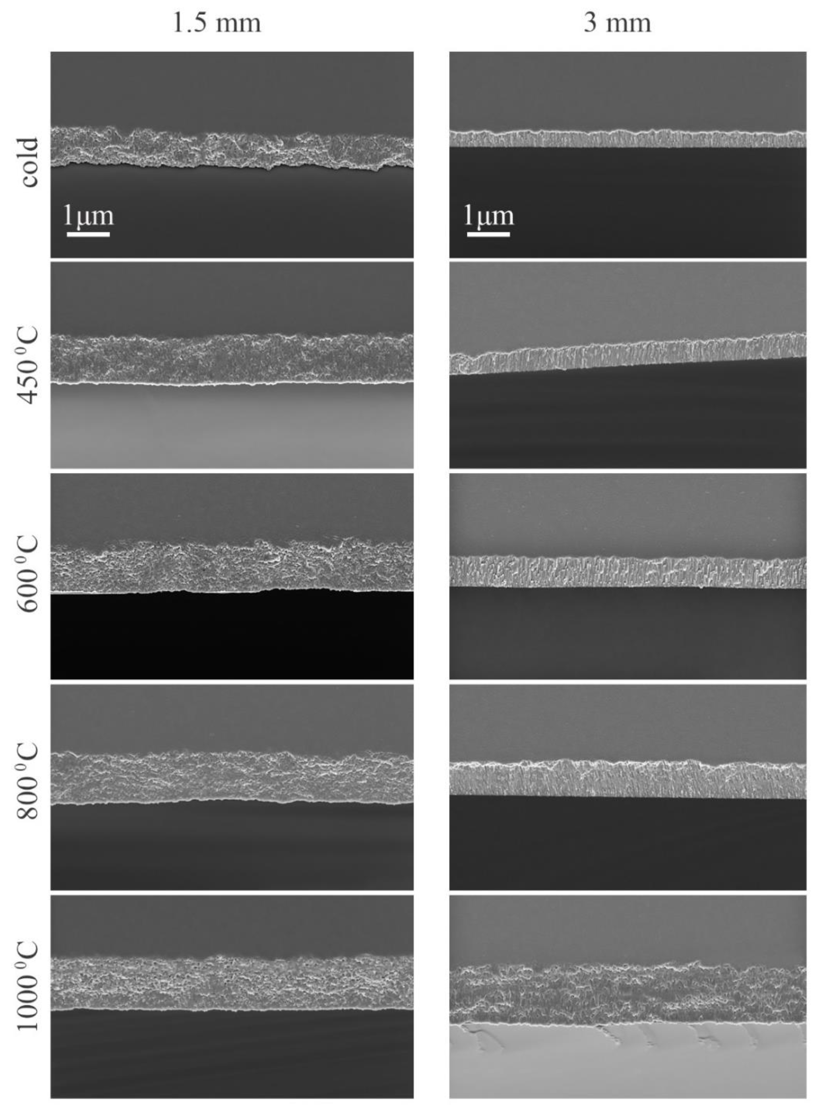
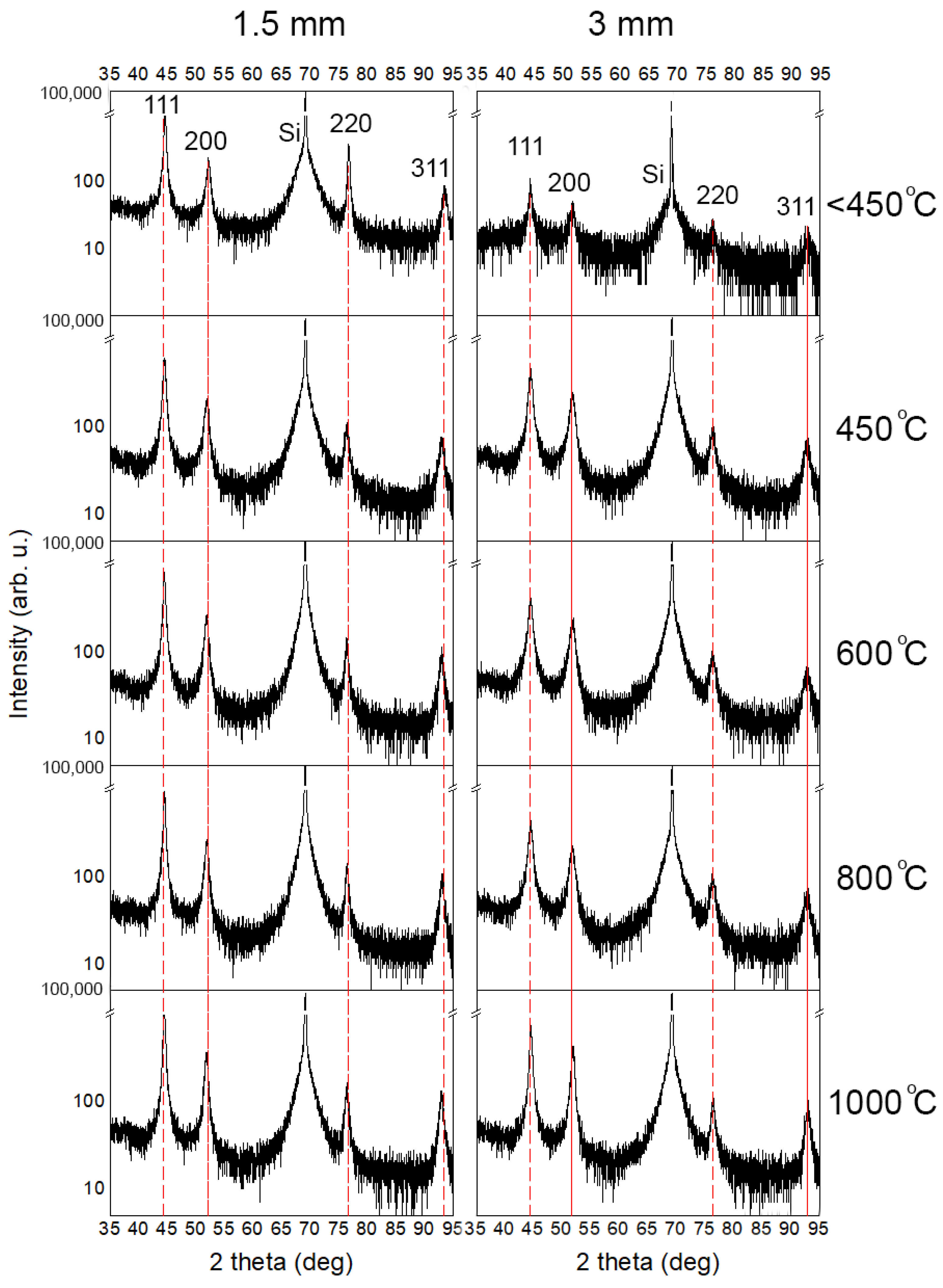
3.2. Coatings Characterization

The SEM images of the nickel coatings’ structure was shown in Figure 6. SEM investigations show the structural morphology of the deposited coatings and their thickness. The structure of the coatings is columnar, typical for the magnetron sputtering method [32,33]. In some cases, it is difficult to observe the columnar structure, probably due to the plastic deformation during the cracking, despite prior freezing by liquid nitrogen. Thickness results read from the images are shown in Table 3.
The conclusion that comes immediately to mind is that the coatings deposited by sputtering a 3 mm nickel target are characterized by a smaller thickness than those obtained with a thinner target. As expected, the thin nickel target sputters more efficiently than the thick target. The effect of the transformation of ferromagnetic to non-magnetic material is mainly evident in the case of the thick target. The growth kinetics in its case increased by 200%, while the thin target increased by only 22%. There is a noticeable increase in the thickness of coatings from a temperature of 450 °C in both cases. Previous results indicated that the best thickness results could be expected at 450 °C. However, it seems that the effects of high discharge energies and the presence of energetic particles in the plasma cannot be combined with the density of the particle flux emitted from the targets. The jet of sputtered particles is enriched with sublimated particles. These, in turn, are low-energy and do not participate in the processes of ionization and internal excitation, which is why previous studies have not considered their contribution to the population.
XRD technique was used to examine the structure of the coatings in more detail. Figure 7 shows a comparison of the diffraction patterns of the fabricated coatings. We have limited the image to the coatings deposited by sputtering 1.5 and 3 mm nickel targets for presentation purposes. Diffraction patterns are very similar to each other. Reflections from the same set of crystallographic planes were identified in all coatings. XRD peaks were used to calculate the size of the crystallites, according to equation 1. The averaged values of the crystallite size are shown in Table 4.
A certain consistency can be seen in the results, in which the smallest crystallites presented layers fabricated at mid-range temperature. Previous studies have suggested that plasma species may have the highest energy under such conditions. This is reflected in the structure and size of the crystallites. It is known that the coating tends to defect and defragment the crystallites during growth under energetic particles bombardment [34]. Above this temperature, an increase in size is observed. This may be due to the increased fraction of low-energy particles originating from sublimation.

4. Conclusions

In this article, we have attempted to actively employ the technological parameters of the GIMS technique to control the temperature in the HTMS process of nickel targets. The period of plasma pulses distribution was a parameter by which we could precisely establish the sputtering temperature. As part of the experiment, we attempted to characterize the sputtering process of a temperature-controlled target, and as we expected, the most significant increase in growth kinetics was observed for the highest temperatures. Our experiment also showed that the sputtering model of ferromagnetic targets at temperatures slightly above TC is exciting and worthy of closer study. From our preliminary findings, one may be inclined to the thesis that this temperature range may be the most favorable for the generation of plasmas whose particles have the highest energies. In this temperature range, we recorded the highest-energy discharges, and the OES spectrum of the plasma excited under these conditions was most enriched with excited particles of sputtered nickel. The preservation of high energy of plasma particles during film fabrication is one of the most raised issues in the literature. Acquiring control over the execution of HTMS processes is a crucial skill in mastering this important parameter of the plasma state. The GIMS technique, at its current stage of development, seems to enable this satisfactorily. As a result, we can use this tool in our future research plans.

Author Contributions

Conceptualization, R.C. and B.W.; methodology, R.C. and B.W.; formal analysis, R.C.; investigation, R.C., K.N.-L., R.M., and M.D.-U.; resources, B.W.; data curation, R.C. and M.D.-U.; writing—original draft preparation, R.C.; writing—review and editing, R.C.; visualization, R.C.; supervision, R.C.; project administration, K.Z.; funding acquisition, K.Z. All authors have read and agreed to the published version of the manuscript.

Funding

This research was funded by the National Science Centre (grant no. 2018/31/B/ST8/00635).

Institutional Review Board Statement

Not applicable.

Informed Consent Statement

Not applicable.

Data Availability Statement

Data is contained within the article.

Conflicts of Interest

The authors declare no conflict of interest.

References

  1. Wolfe, J.C.; He, W.-S.; Licon, D.L.; Chau, R.Y. Ion Assisted Deposition Process with Reactive Source Gassification. U.S. Patent 5,415,756, 16 May 1995. [Google Scholar]
  2. Chau, R.Y.; He, W.-S.; Wolfe, J.C.; Licon, D.L. Effect of target temperature on the reactive d.c.-sputtering silicon and niobium oxides. Thin Solid Films 1996, 287, 57–64. [Google Scholar] [CrossRef]
  3. Bleykher, G.A.; Borduleva, A.O.; Krivobokov, V.P.; Sidelev, D.V. Evaporation factor in productivity increase of hot target magnetron sputtering systems. Vacuum 2016, 132, 62–69. [Google Scholar] [CrossRef]
  4. Sidelev, D.V.; Bleykher, G.A.; Bestetti, M.; Krivobokov, V.P.; Vicenzo, A.; Franz, S.; Brunella, M.F. A comparative study on the properties of chromium coatings deposited by magnetron sputtering with hot and cooled target. Vacuum 2017, 143, 479–485. [Google Scholar] [CrossRef]
  5. Karzin, V.V.; Komlev, A.E.; Karapets, K.I.; Lebedev, N.K. Simulation of heating of the target during high-power impulse magnetron sputtering. Surf. Coat. Technol. 2018, 334, 269–273. [Google Scholar] [CrossRef]
  6. Tesař, J.; Rezek, J.M. On surface temperatures during high power pulsed magnetron sputtering using a hot target. Surf. Coat. Technol. 2011, 206, 1155–1159. [Google Scholar] [CrossRef]
  7. Bleykher, G.A.; Sidelev, D.V.; Grudinin, V.A.; Krivobokov, V.P.; Bestetti, M. Surface erosion of hot Cr target and deposition rates of Cr coatings in high power pulsed magnetron sputtering. Surf. Coat. Technol. 2018, 354, 161–168. [Google Scholar] [CrossRef]
  8. Grudinin, A.; Bleykher, G.A.; Sidelev, D.V.; Krivobokov, V.P.; Bestetti, M.; Vicenzo, A.; Franz, S. Chromium films deposition by hot target high power pulsed magnetron sputtering: Deposition conditions and film properties. Surf. Coat. Technol. 2019, 375, 352–362. [Google Scholar] [CrossRef]
  9. Sidelev, D.V.; Bleykher, G.A.; Krivobokov, V.P.; Koishybayeva, Z. High-rate magnetron sputtering with hot target. Surf. Coat. Technol. 2016, 308, 168–173. [Google Scholar] [CrossRef]
  10. Chodun, R.; Nowakowska-Langier, K.; Zdunek, K.; Okrasa, S. The role of magnetic energy on plasma localization during the glow discharge under reduced pressure. Nukleonika 2016, 61, 191–194. [Google Scholar] [CrossRef] [Green Version]
  11. Meckel, B.B. Magnetic Target Plate for Use in Magnetron Sputtering of Magnetic Films. U.S. Patent No. 4,299,678, 10 November 1981. [Google Scholar]
  12. Ho, K.K.; Carman, G.P. Sputter deposition of NiTi thin film shape memory alloy using a heated target. Thin Solid Films 2000, 370, 18–29. [Google Scholar] [CrossRef]
  13. Loch, D.A.; Gonzalvo, Y.A.; Ehiasarian, A.P. Nickel coatings by inductively coupled impulse sputtering (ICIS). Surf. Coat. Technol. 2015, 267, 98–104. [Google Scholar] [CrossRef] [Green Version]
  14. Brewer, J.A.; Migliuolo, M.; Belan, R.M. Magnetron sputter deposition of magnetic materials from thick targets. Proc. Annu. Tech. Conf. Soc. Vac. Coaters. 1990, 33, 37–42. [Google Scholar]
  15. Chang, S.A.; Skolnik, M.B.; Altman, C. High rate sputtering deposition of nickel using dc magnetron mode. J. Vac. Sci. Technol. A 1986, 4, 413–416. [Google Scholar] [CrossRef]
  16. Wegmann, U. A Cathode Arrangement for the Erosion of Material of a Target in an Apparatus for Cathodic Sputter Coating. G.B. Patent No. 2,090,872, 10 November 1983. [Google Scholar]
  17. Sidelev, D.V.; Bleykher, G.A.; Grudinin, V.A.; Krivobokov, V.P.; Bestetti, M.; Syrtanov, M.S.; Erofeev, E.V. Hot target magnetron sputtering for ferromagnetic films deposition. Surf. Coat. Technol. 2018, 334, 61–70. [Google Scholar] [CrossRef]
  18. Caillard, A.; El’Mokh, M.; Lecas, T.; Thomann, A.L. Effect of the target temperature during magnetron sputtering of nickel. Vacuum 2018, 147, 82–91. [Google Scholar] [CrossRef]
  19. Chodun, R.; Dypa, M.; Wicher, B.; Nowakowska-Langier, K.; Okrasa, S.; Minikayev, R.; Zdunek, K. The sputtering of titanium magnetron target with increased temperature in reactive atmosphere by gas injection magnetron sputtering technique. Appl. Surf. Sci. 2022, 574, 151597. [Google Scholar] [CrossRef]
  20. Chodun, R.; Nowakowska-Langier, K.; Wicher, B.; Okrasa, S.; Kwiatkowski, R.; Zaloga, D.; Dypa, M.; Zdunek, K. The state of coating–substrate interfacial region formed during TiO2 coating deposition by Gas Injection Magnetron Sputtering technique. Surf. Coat. Technol. 2020, 398, 126092. [Google Scholar] [CrossRef]
  21. Chodun, R.; Nowakowska-Langier, K.; Wicher, B.; Okrasa, S.; Minikayev, R.; Dypa, M.; Zdunek, K. TiO2 coating fabrication using gas injection magnetron sputtering technique by independently controlling the gas and power pulses. Thin Solid Films 2021, 728, 138695. [Google Scholar] [CrossRef]
  22. Gencoa: Balanced and Unbalanced. Available online: https://www.gencoa.com/balance-unbalance (accessed on 26 June 2022).
  23. Pawlak, W.; Jakubowska, M.; Sobczyk-Guzenda, A.; Makówka, M.; Szymanowski, H.; Wendler, B.; Gazicki-Lipman, M. Photo activated performance of titanium oxide coatings deposited by reactive gas impulse magnetron sputtering. Surf. Coat. Technol. 2018, 349, 647–654. [Google Scholar] [CrossRef]
  24. Posadowski, W.M.; Wiatrowski, A.; Dora, J.; Radzimski, Z.J. Magnetron sputtering process control by medium-frequency power supply parameter. Thin Solid Films 2008, 516, 4478–4482. [Google Scholar] [CrossRef]
  25. Dora, J. Resonant Power Supply. Polish Patent 313150, 6 March 1996. [Google Scholar]
  26. Palmero, A.; Rudolph, H.; Habraken, F.H. Study of the gas rarefaction phenomenon in a magnetron sputtering system. Thin Solid Films 2006, 515, 631–635. [Google Scholar] [CrossRef]
  27. Huo, C.; Raadu, M.A.; Lundin, D.; Gudmundsson, J.T.; Anders, A.; Brenning, N. Gas rarefaction and the time evolution of long high-power impulse magnetron sputtering pulses. Plasma Sources Sci. Technol. 2012, 21, 045004. [Google Scholar] [CrossRef]
  28. Horwat, S.; Anders, A. Compression and strong rarefaction in high power impulse magnetron sputtering discharges. J. Appl. Phys. 2010, 108, 123306. [Google Scholar] [CrossRef] [Green Version]
  29. Palmero, A.; Rudolph, H.; Habraken, F.H. Gas heating in plasma-assisted sputter deposition. Appl. Phys. Lett. 2005, 87, 071501. [Google Scholar] [CrossRef]
  30. Ganesan, R.; Murdoch, B.J.; Treverrow, B.; Ross, A.E.; Falconer, I.S.; Kondyurin, A.; McCulloch, D.G.; Partridge, J.G.; McKenzie, D.R.; Bilek, M. The role of pulse length in target poisoning during reactive HiPIMS: Application to amorphous HfO2. Plasma Sources Sci. Technol. 2015, 24, 035015. [Google Scholar] [CrossRef]
  31. Meggers, W.F.; Corliss, C.H.; Scribner, B.F. Tables of Spectral-Line Intensities, Part I – Arranged by Elements, Part II—Arranged by Wavelengths. Nat. Bur. Stand. U.S. 1975, 600. [Google Scholar] [CrossRef]
  32. Thornton, J. Influence of apparatus geometry and deposition conditions on the structure and topography of thick sputtered coatings. J. Vac. Sci. Technol. 1974, 11, 666. [Google Scholar] [CrossRef]
  33. Messier, R.; Giri, A.P.; Roy, R.A. Revised structure zone model for thin films physical structure. J. Vac. Sci. Technol. A 1984, 2, 500. [Google Scholar] [CrossRef]
  34. Anders, A. A structure zone diagram including plasma-based deposition and ion etching. Thin Solid Films 2010, 518, 4087. [Google Scholar] [CrossRef] [Green Version]
Figure 1. Diagram illustrating: (a) the apparatus configuration, (b) construction of the hot target system, (c) the heat transfer through the standard (left) and hot (right) target system, (d) plasma pulse distribution over the time.
Coatings 12 01022 g001
Figure 2. Diagram presenting the evolution of glow discharge power during the sputtering of hot nickel target and images of temperature distribution on the target surface.
Coatings 12 01022 g002
Figure 3. Distribution of B at the surface of nickel targets with various thickness and characteristics of plasma pulse energy during the sputtering process.
Coatings 12 01022 g003
Figure 4. Current waveforms measured during the sputtering of 1.5 mm nickel target at various temperatures.
Coatings 12 01022 g004
Figure 5. OES spectrum of plasma registered and fitted with basic components during the sputtering of nickel target (a) and collection of OES spectra registered at various temperatures (b).
Coatings 12 01022 g005
Figure 6. SEM images of nickel coatings structures deposited during the sputtering at various temperatures.
Coatings 12 01022 g006
Figure 7. Diffraction patterns of nickel coatings deposited in the experiment.
Coatings 12 01022 g007
Table 1. Parameters of hot nickel target sputtering in the experiment.
Target Thickness (mm)TemperaturePeriod (ms)Deposition Time (s)
1.5<4502000720
4501300468
6001150414
800900324
1000650234
2<4502000720
4501500540
6001100396
800900324
1000650234
2.5<4502000720
4501100396
600730263
800580209
1000550198
3<4502000720
4501500540
6001000360
800650234
1000550198
Table 2. OES lines attributed to the measured spectra [31].
SpecieWavelength (nm)Rel. IntensityLower LevelUpper Level
Ni I349.355003d9(2D)4s3d9(2D)4p
Ni I351.026003d9(2D)4s3d9(2D)4p
Ni I351.566003d9(2D)4s3d9(2D)4p
Ni I352.482003d9(2D)4s3d9(2D)4p
Ni I353.211003d8(3F)4s23d9(2D)4p
Table 3. Nickel coatings thickness deposited during the HTMS processes.
1.5 mm Thick Target3 mm Thick TargetTemperature (°C)
900 nm380 nm<450
950 nm500 nm450
1070 nm640 nm600
1080 nm680 nm800
1100 nm1140 nm1000
Table 4. Averaged crystallites’ size of nickel coatings deposited in experiment.
1.5 mm Thick Target3 mm Thick TargetTemperature (°C)
7.8 nm18.2 nm<450
7.3 nm10.2 nm450
7.2 nm13.1 nm600
7.7 nm15.2 nm800
12.6 nm15.0 nm1000
Publisher’s Note: MDPI stays neutral with regard to jurisdictional claims in published maps and institutional affiliations.

