Article

Bi Layer Properties in the Bi–FeNi GMR-Type Structures Probed by Spectroscopic Ellipsometry

1
Lebedev Physical Institute, Russian Academy of Sciences, Leninsky Prospect 53, 119991 Moscow, Russia
2
Institute of Physics, Academy of Sciences of the Czech Republic, Na Slovance 2, 18221 Prague, Czech Republic
*
Authors to whom correspondence should be addressed.
Coatings 2022, 12(6), 872; https://doi.org/10.3390/coatings12060872
Submission received: 18 May 2022 / Revised: 13 June 2022 / Accepted: 17 June 2022 / Published: 20 June 2022
(This article belongs to the Special Issue Recent Advances in the Growth and Characterizations of Thin Films)

Abstract

:
Bismuth (Bi) having a large atomic number is characterized by a strong spin–orbit coupling (SOC) and is a parent compound of many 3D topological insulators (TIs). The ultrathin Bi films are supposed to be 2D TIs possessing a nontrivial topology, which opens the possibility of developing new efficient technologies in the field of spintronics. Here we aimed at studying the dielectric function properties of ultrathin Bi/FeNi periodic structures using spectroscopic ellipsometry. The [Bi(d)–FeNi(1.8 nm)] N GMR-type structures were grown by rf sputtering deposition on Sitall-glass (TiO 2 ) substrates. The ellipsometric angles Ψ ( ω ) and Δ ( ω ) were measured for the grown series (d = 0.6, 1.4, 2.0, and 2.5 nm, N = 16) of the multilayered film samples at room temperature for four angles of incidence of 60 , 65 , 70 , and 75 in a wide photon energy range of 0.5–6.5 eV. The measured ellipsometric angles, Ψ ( ω ) and Δ ( ω ) , were simulated in the framework of the corresponding multilayer model. The complex (pseudo)dielectric function spectra of the Bi layer were extracted. The GMR effects relevant for the studied Bi–FeNi MLF systems were estimated from the optical conductivity zero-limit (optical GMR effect). The obtained results demonstrated that the Bi layer possessed the surface metallic conductivity induced by the SOC effects, which was strongly enhanced on vanishing the semimetallic-like phase contribution on decreasing the layer thickness, indicating its nontrivial 2D topology properties.

1. Introduction

The relativistic effect of spin–orbit (SOC) coupling is involved in the so-called Rashba effect [1]. This phenomenon arises from the apparent loss of crystalline inversion symmetry near the surface or heterojunction leading to the lifting of the spin degeneracy and generating spin-polarized surface metallic states. In this respect, 3D (2D) topological insulators (TIs) also exhibit spin-polarized surface metallic states due to SOC. However, contrary to the Rashba effect, the surface metallic bands of a TI are determined by its bulk characteristics. The TIs host metallic surface states in a bulk energy gap, which are topologically protected. The surface (or interface) states of TIs can be topologically trivial or nontrivial. In the latter case, for example, electrons cannot be backscattered by impurities. Bismuth (Bi), having a large atomic number, is characterized by a strong SOC and is a parent compound of many 3D TIs, such as Bi 1 x Sb x or Bi 2 Se 3 , even though 3D bulk Bi itself is topologically trivial. The specific feature of the electronic band structure of bulk Bi having R 3 ¯ m rhombohedral symmetry [2,3,4] is its inverted band gaps at both the Γ and M points of the Brillouin zone due to the strong SOC. The uniqueness of Bi films associated with surface metallic states [5,6] and the semiconductor-to-metal transition [7,8] are well documented in the literature.
Theoretical analyses predict a 1-bilayer (BL) Bi(111) film to be a 2D TI [9,10]. If there is no or weak inter-BL coupling, a stack of the odd–even 1-BL films will exhibit nontrivial to trivial oscillations of topology (where the topological number ν [11] is equal to 1 or 0, respectively). However, for the nontrivial topology in a stack of 1-BL films, the intermediate inter-BL coupling strength, which is, for example, higher than the van der Waals strengths, is a mandatory condition. The direct ( Γ point) and indirect band gap values were calculated by Liu et al. as a function of the Bi film thickness [12]. It was established that below four BLs the film is a semiconductor with the direct gap open at the Γ point and the positive indirect band gap leading to nontrivial topology characteristic of an intrinsic 2D TI. Above four BLs the indirect band gap becomes negative resulting in a semiconductor– semimetal transition due to the overlapping of two bands at the Fermi level around the Γ and M points. This suggests that the Bi films from five to eight BLs represent a 2D TI situated between two trivial metallic surfaces [12].
A comprehensive study of the associated SOC effects in ultrathin Bi layers opens the possibility of developing new efficient technologies in the field of spintronics. For this purpose, here we aimed at studying the dielectric function properties of ultrathin periodic structures Bi/Ni 79 Fe 21 , prepared by rf sputter deposition, which is one of the most common technologies used to grow coatings and multilayered films (MLFs) exhibiting a giant magnetoresistance (GMR) effect for various existing and modern nanotechnological applications. In earlier work, we demonstrated that the electronic band structure and surface electronic properties of ultrathin Bi layers in real GMR-type (Bi–FeNi) N MLF structures incorporating nanoisland FeNi layers could be successfully studied by spectroscopic ellipsometry (SE) [13]. Here, by applying the elaborated SE approach, we investigated (Bi–FeNi) MLFs, where the thickness of the FeNi layer was 1.8 nm, corresponding to the FeNi layer structural percolation threshold [14,15], and the Bi spacer layer was 0.6, 1.4, 2.0, and 2.5 nm thick, incorporating about two, four, six, and eight Bi 012 -type planes, respectively. We found that the Bi spacer layers have a metallic surface conductivity, which demonstrates strongly enhanced metallicity properties on vanishing the Bi semimetallic-like phase contribution on decreasing the layer thickness, which can be constructive in finding new nontrivial 2D topology properties of the (Bi–FeNi) GMR-type structures for their different nanotechnological applications.

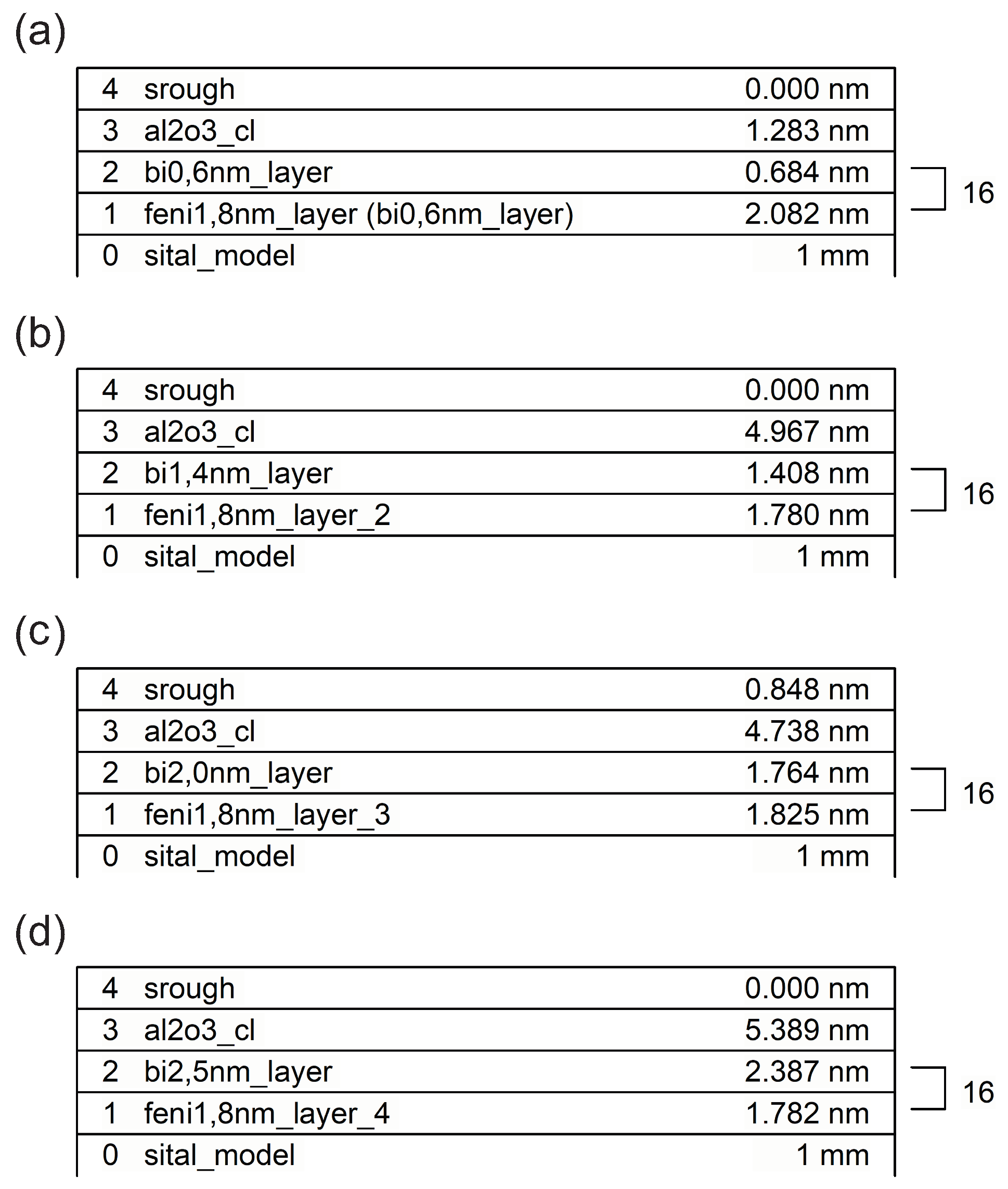
2. Materials and Methods

The (Bi–FeNi) N MLFs were prepared in a sputter deposition system by cathode sputtering from 99.95% pure Bi and Fe 21 Ni 79 targets in an alternative way. The base pressure in a sputter deposition chamber was 2 × 10 6 Torr. The multilayers were deposited at approximately 80 C in an argon atmosphere of 6 × 10 4 Torr on insulating glassy Sitall (TiO 2 ) substrates. We utilized the substrates having typical dimensions 15 × 5 × 0.6 mm 3 . The nominal thicknesses of the FeNi and Bi layers were controlled by the layer deposition times in accordance with the material deposition rates. A series consisting of four MLF samples was prepared. In the series of the grown (Bi–FeNi) N samples, the nominal thickness of the FeNi layer was 1.8 nm, the Bi layer thickness was 0.6, 1.4, 2.0, and 2.5 nm, and the number N of periodically repeated Bi/FeNi layers was 16. The thickness of the FeNi layer was chosen to be 1.8 nm, matching the structural percolation threshold [14,15]. The Bi layer thicknesses were chosen in such a way that the conditions for ferromagnetic (FM) or antiFM coupling in the GMR-type structures would be optimized. To prevent degradation of the MLFs, the deposited (Bi–FeNi) 16 –FeNi/Sitall samples were covered in situ with a 2.1 nm thick Al 2 O 3 capping layer.
The related [Bi–FeNi(0.8, 1.2 nm)] N samples prepared by rf sputtering deposition onto the Sitall substrates under similar conditions were investigated by X-ray diffraction (XRD) as well as by the X-ray reflectivity (XRR) experimental techniques from our previous study (see Supplementary online information for the article [13]). The XRR spectra proved to have a good periodicity and consistency with the corresponding nominal thicknesses of the FeNi and Bi slices in the Bi/FeNi MLF structures, as well as a relatively low interface roughness between the constituent layers. The XRD characterization suggested a (012)-type Bi plane orientation, where the interlayer distance was 3.28 Å. It followed from this that in the studied MLF structures, the Bi layers with a thickness corresponding to 0.6, 1.4, 2.0, and 2.5 nm incorporated two, four, six, and eight Bi(012)-type planes, respectively.
In the present study, the surface morphology of the Bi–FeNi(1.8 nm) MLF samples, prepared by rf sputtering deposition on the Sitall (TiO 2 ) substrates, was studied at room temperature using an ambient AFM (Bruker, Dimension Icon) in the PeakForce Tapping mode with ScanAsyst-Air tips (Bruker, k = 0.4 N/m, nominal tip radius 2 nm). The SE measurements for the investigated Al 2 O 3 /(Bi–FeNi) 16 /Sitall samples were performed at room temperature in a wide photon energy range of 0.5–6.5 eV using a J.A. Woollam VUV–VASE ellipsometer (see the scheme illustrating the SE study of the (Bi–FeNi) N MLFs in Ref. [13], Figure 1a). The measured ellipsometry spectra are represented by real values of the angles Ψ ( ω ) and Δ ( ω ) , which are defined through the complex Fresnel reflection coefficients for light-polarized parallel r p and perpendicular r s to the plane of incidence, tan Ψ e i Δ = r p r s . The ellipsometric angles, Ψ ( ω ) and Δ ( ω ) , measured for the Bi–FeNi MLF samples were simulated using the multilayer model simulation available in J.A. Woollam VASE software [16]. From the multilayer model simulations, the (pseudo)dielectric function spectra of the ultrathin 0.6, 1.4, 2.0, and 2.5 nm Bi layers and 1.8 nm FeNi layer inside the Bi–FeNi MLF structures were extracted. The corresponding calculated optical conductivity spectra were analyzed.

3. Results

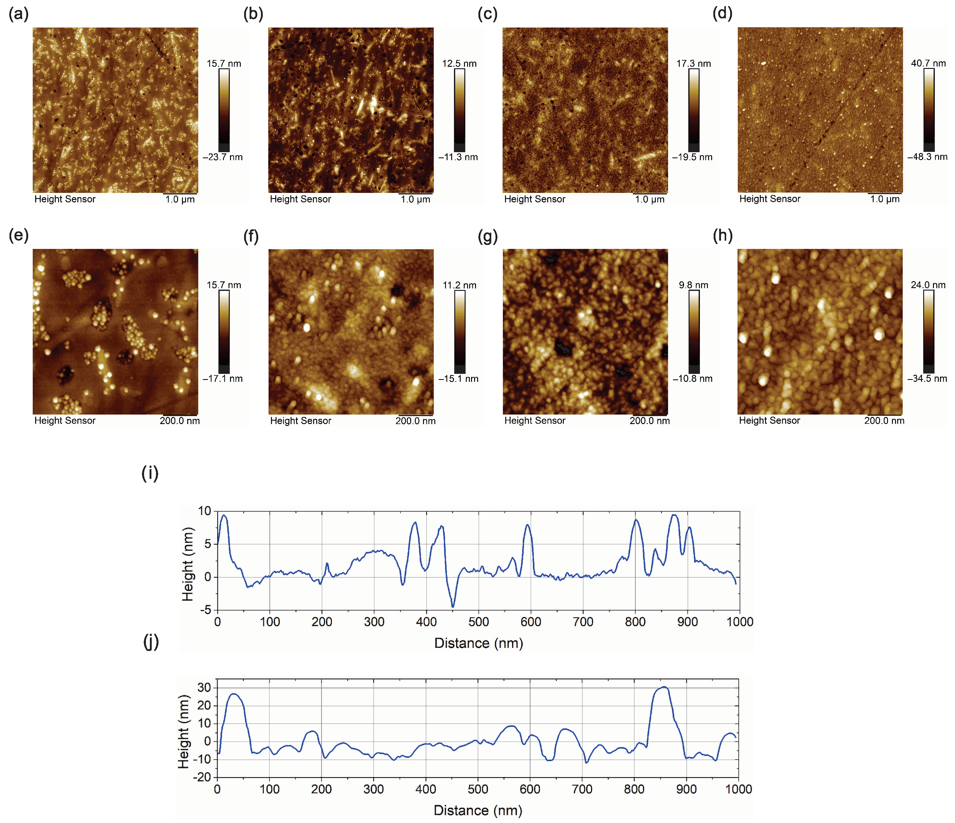
3.1. Atomic Force Microscopy Study

The retrieved 5 × 5 μ m 2 and 1 × 1 μ m 2 AFM images of the Al 2 O 3 (2.1 nm)/[Bi(0.6, 1.4, 2.0, 2.5 nm)–FeNi(1.8 nm)] N /Sitall multilayered films (where the given layer thicknesses correspond to their nominal values) presented in Figure 1a–h show a discernible contrast because of the available surface height deviations. The surface roughness of the Sitall glass (TiO 2 ) substrates was investigated by AFM in our earlier publication [17]. The height profile of the Sitall substrates (see Ref. [17], Figure 2a) demonstrated a height deviation within the range 1–3 nm characteristic of the relatively large 0.3–1 μ m lateral scale, which characterizes the Sitall substrate surface roughness. From the AFM measurements on the areas 5 × 5 μ m 2 and 1 × 1 μ m 2 the root-mean square (RMS) surface roughness values were evaluated, which are presented in the caption to Figure 1. The corresponding RMS roughness values are notably higher for the Al 2 O 3 (2.1 nm)/[Bi(2.5 nm)–FeNi(1.8 nm)] 16 /Sitall MLF sample. The smaller-scale (1 × 1 μ m 2 ) images clearly exhibit a fine grainy-like structure of the surface morphology, which seems to be characteristic for all studied film samples (see Figure 1e–h). The typical grain size, of about 50 nm, is notably larger for the FeNi(1.8 nm)-Bi MLF sample incorporating the 2.5 nm thick Bi layers, and, following the estimated RMS roughness values, the average grain size decreases to about 20 nm when decreasing the Bi layer thickness to 1.4 nm. As one can see from the typical height profiles presented in Figure 1i,j, when decreasing the Bi layer thickness from 2.5 to about 0.6 nm, the surface morphology becomes highly irregular due to the formation of conglomerates of nanoislands separated by rather flat (relatively small roughness) areas of about 20 nm.

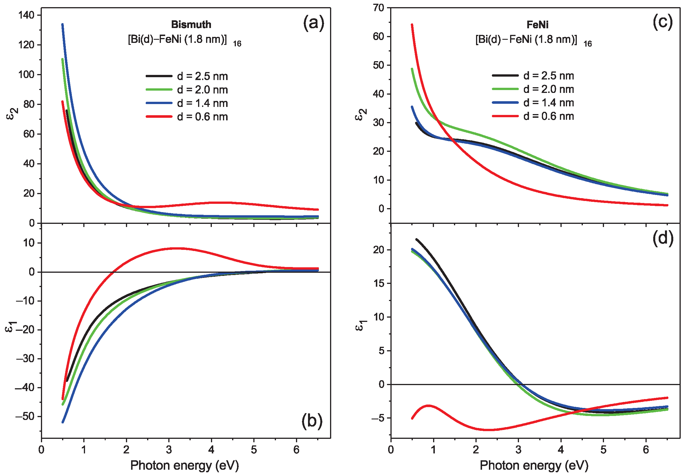
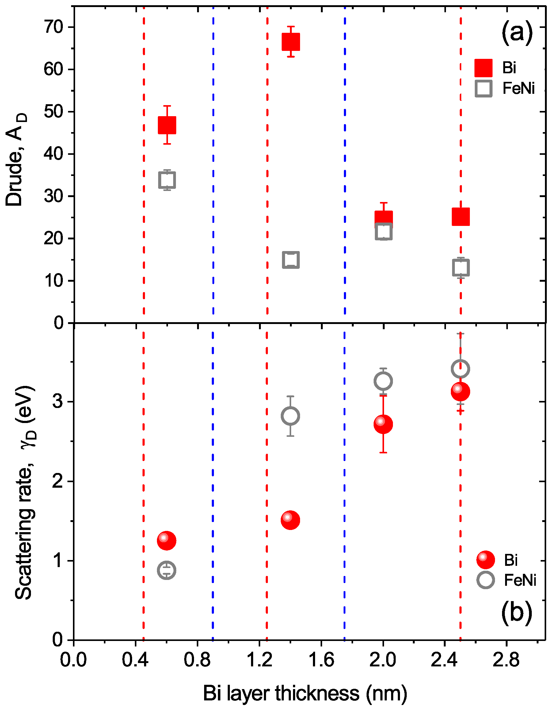
3.2. Spectroscopic Ellipsometry Study of the Ultrathin Bi–FeNi Multilayer Film Samples

The ellipsometric angles Ψ ( ω ) and Δ ( ω ) were measured for the prepared Al 2 O 3 /(Bi–FeNi) 16 /Sitall MLF samples at the angles of incidence of 60 , 65 , 70 , and 75 . Figure 2 demonstrates the ellipsometric angles Ψ ( ω ) and Δ ( ω ) recorded at 65 and 70 . To model the contributions from free charge carriers and interband optical transitions, the complex dielectric function ε ˜ ( ω ) = ε 1 ( ω ) + i ε 2 ( ω ) of the Bi and FeNi layers was interpreted in terms of the Drude and Lorentz parts, respectively,
ε ˜ ( E ω ) = ϵ A D E 2 + i E γ D + j A j γ j E j E j 2 E 2 i E γ j ,
where ε is the high-frequency dielectric constant, which takes into account the contribution from the higher-energy interband transitions. The fitted Drude parameters were A D and the free charge carrier’s scattering rate γ D . The fitted parameters of Lorentz bands were E j , γ j , and A j of the band maximum energy, the full width at half-maximum, and the ε 2 band height, respectively. The obtained ellipsometric angles Ψ ( ω ) and Δ ( ω ) measured at different angles of incidence of 60 , 65 , 70 , and 75 were fitted for each sample simultaneously using J.A. Woollam VASE software [16] in the framework of the designed multilayer model. The multilayer model for the studied Al 2 O 3 /(Bi–FeNi)/Sitall multilayers was constructed as it is schematically presented in Figure 3, exactly so, as the layers were deposited. In addition, we attempted to take into account the roughness properties of the surface by using the conventional approach of effective medium approximation (EMA) based on the (50% Al 2 O 3 –50% vacuum) Bruggeman model. The dispersion model for the Bi layers included three or four Lorentz terms as well as the Drude part. The dispersion model for the 1.8 nm permalloy layers incorporated in the studied MLF structures included the Drude term responsible for the free charge carrier contribution and one Lorentz oscillator to account for the most pronounced interband optical transition. In addition, the dielectric function spectra of the bare Sitall substrate derived from our earlier SE studies [18,19] were introduced to the elaborated multilayer model. The dielectric response of the Al 2 O 3 capping layer was represented by the tabular complex dielectric function spectra [20]. The thicknesses of the Bi and FeNi layers, as well as of the surface layers, were fitted. The unknown parameters were allowed to vary until the minimum of the mean squared error (MSE) was reached. The best simulation result for the studied [Bi(0.6, 1.4, 2.0, 2.5 nm)–FeNi(1.8 nm)] 16 MLF samples corresponded to the lowest obtained MSE values of 0.3843, 0.297, 0.2934, and 0.4508, respectively. The good quality of the fit allowed us to estimate the actual Bi and FeNi layer thicknesses in the MLFs under study. The quality of the fit is demonstrated by Figure 2, where we plotted the measured ellipsometric angles along with the simulation results. The Drude and Lorentz parameters resulting from the simulation of the Al 2 O 3 /[Bi(d)–FeNi(1.8 nm)] 16 /Sitall MLF samples are given in Table 1 and Table 2, and the resulting ε 1 ( ω ) and ε 2 ( ω ) parts of the Bi and FeNi (pseudo)dielectric function spectra are presented in Figure 4.
From Figure 4a,b one can see that the complex (pseudo)dielectric functions of the 0.6, 1.4, 2.0, and 2.5 nm thick Bi spacers inside the investigated Bi–FeNi MLFs demonstrate a metallic character. Moreover, the ε 1 ( ω ) function progressively decreases while the Bi thickness decreases from 2.5 to 2.0 to 1.4 nm and the ε 2 ( ω ) increases at low photon energies, respectively. According to our simulation results, we expect that the best metallicity properties are demonstrated by the Bi layer in the [Bi(1.4 nm)–NiFe(1.8 nm)] 16 structure. At the same time, the complex (pseudo)dielectric functions of the thinnest 0.6 nm thick Bi layer look somewhat different. Here, in addition to the low-energy metallic Drude response identified by the characteristic behavior of ε 1 ( ω ) and ε 2 ( ω ) , the Lorentz band around 4–5 eV makes an essential contribution to the dielectric function response (the corresponding Drude ( A D and γ D ) and Lorentz ( A j , E j , and γ j ) parameters are listed in Table 1). Next, being similar, the dielectric functions of the 1.8 nm thick permalloy layers in the [FeNi–Bi(1.4, 2.0, 2.5 nm)] MLFs are dominated by the ε 2 ( ω ) resonance and ε 1 ( ω ) antiresonance features, indicating the predominant contribution from the Lorentz oscillator peaking at around 3 eV (see Figure 4c,d). An upturn evident in the ε 2 ( ω ) at low photon energies indicates an additional Drude contribution, which is relatively less pronounced. Following our simulation results, we expect the advanced metallicity properties of the FeNi layer in the [Bi(0.6 nm)–NiFe(1.8 nm)] 16 structure (see the corresponding Drude ( A D and γ D ) and Lorentz ( A j , E j , and γ j ) parameters listed in Table 2).
Figure 5a–d present the evolution of the Bi intralayer optical conductivity, σ 1 ( ω ) = ε 2 ( ω ) ω (cm 1 )/60, upon decreasing the Bi spacer layer thickness in the [FeNi(1.8 nm)–Bi(2.5, 2.0, 1.4, 0.6 nm)] 16 structures, and Figure 5e–h show the associated optical conductivity spectra of the 1.8 nm FeNi permalloy layer. Here, the contributions from the Drude and Lorentz oscillators following the multilayer model simulations using Equation (1) are evidently demonstrated. The presented optical conductivity spectra of the Bi and FeNi layers follow the main trends identified in their complex dielectric function spectra presented in Figure 4.

4. Discussion

Initially, we would like to discuss the GMR effects relevant to the studied MLF systems. Our simulations of the dielectric functions for the 1.8 nm thick NiFe layer inside the [Bi(0.6, 1.4, 2.0, 2.5 nm)–NiFe(1.8 nm)] MLFs showed the presence of the Drude term complemented with the pronounced Lorentz band located at around 2–3 eV (see Table 2). From the corresponding optical conductivity spectra presented in Figure 5e–h one can notice that the associated Drude dc limit, σ 1 ω 0 , displays an oscillating character (in agreement with the results deduced for the corresponding Drude parameter A D , see Table 2 and Figure 6). We can expect that the Bi spacer thicknesses for which the FeNi layers are preferentially antiFM-coupled in the studied MLFs are around 1.4 and 2.5 nm implying that the [Bi(1.4, 2.5 nm)–NiFe(1.8 nm)] 16 film structures will exhibit a drop in resistance (being negative magnetoresistance) when exposed to an external magnetic field. It is well known from the literature that the first antiFM maximum exhibits a negative magnetoresistance of about 20%, while the second antiFM maximum decreases to about 10%, and the presence of the third antiFM maximum cannot confidently be retrieved (see, for example, [21] and references therein). Using a simple model of a two-current series resistor [22], the magnetoresistance Δ R R can be estimated as
Δ R R = 100 % α β 2 4 α + d B i d F e N i β + d B i d F e N i ,
where d B i and d F e N i are the thicknesses of the Bi and FeNi layers, and α = ρ F e N i ρ B i and β = ρ F e N i ρ B i are the ratios of the resistivity in the FeNi layer to that in the Bi layer in the spin down and spin up current channel, respectively. Exploiting values for ρ = σ 1 ω 0 1 estimated for the 1.4 nm Bi and 1.8 nm FeNi layers from the current model simulations (see Table 1 and Table 2), namely, ρ B i = 1 8970 Ω · cm, ρ F e N i = 1 2020 Ω · cm, and ρ F e N i = 1 4540 Ω · cm (the latter estimate is given by the FM coupling for the 0.6 nm Bi spacer), we obtain α = 4.4, and β = 2.0. Then, using Equation (2), we have Δ R R =10%. This means that the 1.4 nm Bi spacer corresponds to the second antiFM maximum. Following the same approach for the 2.5 nm Bi spacer, where ρ B i = 1 3370 Ω · cm, ρ F e N i = 1 1760 Ω · cm and ρ F e N i = 1 2920 Ω · cm (corresponding to the FM coupling for the 2.0 nm Bi spacer), we obtain α = 1.9 and β = 1.2. Using Equation (2), we have Δ R R =1.4%, which may correspond to the very weakly pronounced third antiFM maximum. From the analysis presented above, we may expect that the first antiFM maximum, corresponding to the magnetoresistance of about 20%, occurs for the Bi spacer thickness of about 0.9 nm, which is in agreement with the results presented in [21].
Further, in the XRD patterns of the investigated Al 2 O 3 /[Bi(1.4, 2.0, 2.5 nm)–NiFe(1.8 nm)] 16 /Sitall film samples, the peak of the R 3 ¯ m crystalline Bi phase was identified at 2 θ ≈ 26.2 suggesting a 012 orientation of the Bi layers, which is characterized by the interlayer distance of 3.28 Å. Using STM and reflection high-energy electron diffraction (RHEED) techniques, it was shown that the initial growth of Bi 012 -type films occurs in the form of islands with a height increment of about 6.6 Å, indicating an even-number layer stability leading to the laterally flat morphology of the Bi 012 -type islands [23]. Consequently, we can expect that the 0.6, 1.4, 2.0, and 2.5 nm Bi spacer layers in the investigated MLFs incorporate about two, four, six, and eight 012 -type Bi planes, respectively.
The model simulations for the [Bi(2.5, 2.0 nm)–FeNi(1.8 nm)] 16 film samples revealed that the low-energy dielectric function of the Bi intralayers had competing contributions from the Drude term and from the intense Lorentz band around 0.36–0.39 eV with a ε 2 maximum height of 70–100 (see Table 1). The Drude and Lorentz contributions were more clearly pronounced in the corresponding optical conductivity spectra (see Figure 5a,b). The obtained Drude and Lorentz parameters were in excellent agreement with those deduced in our previous study [13] for the Bi spacer layer incorporated in the [Bi(2.5, 2.0 nm)–FeNi(1.2 nm)] 16 structures under study. The pronounced Lorentz band found at low photon energies for Bi single crystals (rhombohedral symmetry, space group R 3 ¯ m ) [24,25] and bulk Bi layers [26,27] is characteristic of the semimetallic-like electronic band structure due to the contributions from the interband transitions near the Γ point, Γ 6 + Γ 6 and Γ 45 + Γ 6 [2], and near the T point, T 6 – T 45 [4]. The estimated values (see Table 1) of the Drude dc limit σ 1 ω 0 (2750–3830 Ω 1 ·cm 1 ) as well as the free charge carrier’s γ D (2.3–3.3 eV) were consistent with those characteristic of the metallic surface states related to the Rashba SOC in Bi(111) films, σ 1 ω 0 = 2300 Ω 1 ·cm 1 and γ D = 2.0 eV) [6]. Meanwhile, the model simulation for the [Bi(1.4 nm)–FeNi(1.8 nm)] 16 structure indicated that for the 1.4 nm Bi layer, the Drude dc limit significantly increased to 8970 ± 540 Ω 1 ·cm 1 , while the γ D essentially decreased to 1.50 ± 0.06 eV. In this case, the Lorentz band was nearly suppressed. The associated found Drude parameters for the ultrathin Bi layer inside the [Bi(0.6 nm)–FeNi(1.8 nm)] 16 structure were slightly different, namely, σ 1 ω 0 = 6300 ± 540 Ω 1 ·cm 1 and γ D = 1.2 ± 0.1 eV, and the Lorentz band was clearly not present (see Figure 5c,d and Table 1).
Thus, we discovered that, on the one hand, the optical conductivity spectra of the 2.0 and 2.5 nm thick Bi spacer layers in the (Bi–FeNi) MLFs incorporating eight and six Bi 012 -type monolayers, respectively, had contributions from the pronounced low-energy Lorentz oscillator and from the free charge carrier Drude term (for details, see Figure 5a,b and Table 1). Here, the presence of the low-energy Lorentz band points on the Bi semimetallic phase contribution and the parameters obtained for the Drude conductivity indicate that its origin can be associated with the surface metallic states [6]. Therefore, the 2.0 and 2.5 nm Bi layers can be associated with the semimetallic Bi phase sandwiched between two metallic layers on the top and bottom surfaces. On the other hand, the contribution from the intrinsic Lorentz band was strongly suppressed for the 1.4 and 0.6 nm layers, where the Drude conductivity displayed notably improved metallicity properties, as one can see from the optical conductivity spectra shown in Figure 5c,d (for details, see Table 1).
From the above discussion of the obtained results, we can conclude that the Bi layer consisting of four Bi(012)-type monolayers represents a kind of crossover regarding the contributions from the semimetallic Bi phase and/or surface metallic-like states. Here, we notice some similarity with the theory results presented for the ultrathin Bi(111) layers by Liu et al. [12]. In their paper, it was established that below four Bi(111) BLs the film is a semiconductor with a direct gap open at the Γ point and a positive indirect band gap, leading to a nontrivial Z 2 topology ( ν = 1) characteristic of an intrinsic 2D TI. However, above four Bi(111) BLs, the indirect band gap becomes negative resulting in a semiconductor–semimetal transition, due to the overlapping of two bands at the Fermi level around the Γ and M points. It was argued by Liu et al. [12] that the Bi layers consisting of five to eight Bi(111) BLs represented a 2D TI placed between two “trivial” metallic surfaces [12]. This means that for the surface considered as an individual 2D system, its Z 2 number is trivial ( ν = 0). The surface bands have no contribution to the nontrivial Z 2 topology and, therefore, these trivial metallic surfaces are not robust and can easily be removed by surface defects or impurities. We found [13] that the Bi layers in the [Bi(2.0, 2.5 nm)–FeNi(0.8 nm)] multilayers, incorporating the nanoisland permalloy layer, exhibited bulk-like semimetallic properties of the electronic band structure, although the surface (Drude) metallic conductivity was absent there (see Ref. [13], Figure 4d). Indeed, a strong magnetic and spatial disorder induced by magnetic FeNi nanoislands, as well as long-range many-body interactions between the magnetic moments of permalloy nanoislands [17], may lead to a specific localization of free charge carriers [28]. However, the surface conductivity (or interface) states for the 1.4 nm layer in the Bi–FeNi(1.8 nm) multilayers may be topologically nontrivial and, in this case, the electrons cannot be backscattered by impurities. Here, the Drude dc limit was 8970 ± 540 Ω · cm 1 and the scattering rate γ D = 1.5 ± 0.06 eV. We found that the 0.6 nm thick Bi layer exhibited somewhat different Drude dc limit (6300 ± 540 Ω · cm 1 ) and γ D (1.2 ± 0.1 eV), see Table 1 and Figure 6, which can be attributed to the discontinuous nanoisland structure of this layer.
Finally, we would like to note that it will be challenging to investigate the dc transport and superconductivity properties of the ultrathin Bi films possessing 2D TI surface states following the approach presented in [29], where the subkelvin superconductivity without any external stimuli was discovered in 3D TI Cd 3 As 2 films [30,31].

5. Conclusions

In summary, using wide-band (0.5–6.5 eV) spectroscopic ellipsometry, we studied the optical properties of the [Bi(0.6, 1.4, 2.0, 2.5 nm)–FeNi(1.8 ṅm)] 16 MLFs prepared by rf sputtering. The XRD analysis suggested that the 0.6, 1.4, 2.0, and 2.5 nm Bi layers in the studied MLFs corresponded to about two, four, six, and eight Bi 012 -type monolayers, respectively. From the multilayer model simulations of the measured ellipsometric data, we extracted the Bi and FeNi layer dielectric functions. The dielectric function for the 2.0 and 2.5 nm Bi spacer layers were represented by the Drude resonance due to the surface states and the low-energy Lorentz band peaking at around 0.3–0.4 eV. The pronounced Lorentz band was characteristic of the semimetallic bulk-like Bi electronic zone structure due to the contributions from the interband transitions near the Γ point. We discovered that the 2.0 and 2.5 nm Bi spacer layers could be associated with the semimetallic Bi phase sandwiched between two trivial (where the topology number ν = 0) metallic layers on the top and bottom surfaces. The contribution from the low-photon-energy Lorentz band was strongly suppressed for the 1.4 and 0.6 nm Bi layers, where the Drude conductivity displayed notably improved metallicity properties. This indicated that the Bi layer consisting of four Bi 012 -type monolayers represented a kind of crossover regarding the contributions from the semimetallic Bi phase and/or surface metallic-like states. Therefore, the properties of Bi layers below four monolayers may be associated with the nontrivial topology (where the topology number ν = 1) characteristic of an intrinsic 2D TI. We expect that the Bi layers having thickness of 0.9 nm will exhibit a maximal GMR effect of about 20% in the (Bi–FeNi) MLFs, where the Drude dc limit is about 8970 ± 540 Ω · cm 1 . These states may be protected from backscattering, which makes them promising in spintronic devices and quantum computing.

Author Contributions

Conceptualization, N.K. and A.D.; methodology, D.C. and L.F.; validation, N.K. and A.D.; investigation, D.C. and N.K.; data curation, D.C. and N.K.; writing—original draft preparation, N.K.; writing—review and editing, N.K. and A.D.; visualization, N.K. and L.F.; supervision, N.K. and A.D.; project administration, A.D.; funding acquisition, A.D. All authors have read and agreed to the published version of the manuscript.

Funding

This work was supported in part by the European Structural and Investment Funds and the Czech Ministry of Education, Youth, and Sports (Project No. SOLID21, Cz 02.1.01/0.0/0.0/16_019/0000760).

Institutional Review Board Statement

Not applicable.

Informed Consent Statement

Not applicable.

Data Availability Statement

Not applicable.

Acknowledgments

We thank F.A. Pudonin for providing us with the Bi/FeNi multilayer film samples and O. Pacherova for their XRD analysis. We thank A. Muratov for participation in the spectroscopic ellipsometry measurements.

Conflicts of Interest

The authors declare no conflict of interest.

Sample Availability

Samples of the Bi/FeNi multilayer films are available from the P.N. Lebedev Physical Institute, Moscow, Russia.

Abbreviations

The following abbreviations are used in this manuscript:
GMRGiant magnetoresistance
SOCSpin–orbit coupling
TITopological insulator
MLFMultilayered film
SESpectroscopic ellipsometry
AFMAtomic force microscopy
FMFerromagnetic
XRDX-ray diffraction
XRRX-ray reflectivity

References

  1. Bychkov, Y.A.; Rashba, E.I. Properties of a 2D electron gas with lifted spectral degeneracy. JETP Lett. 1984, 39, 78–81. [Google Scholar]
  2. Golin, S. Band Structure of Bismuth: Pseudopotential Approach. Phys. Rev. B 1968, 166, 643–651. [Google Scholar] [CrossRef]
  3. Gonze, X.; Michenaud, J.-P.; Vigneron, J.-P. First-principles study of As, Sb, and Bi electronic properties. Phys. Rev. B 1990, 41, 11827–11836. [Google Scholar] [CrossRef] [PubMed] [Green Version]
  4. Liu, Y.; Allen, R.E. Electronic structure of the semimetals Bi and Sb. Phys. Rev. B 1995, 52, 1566–1577. [Google Scholar] [CrossRef] [PubMed] [Green Version]
  5. Hofmann, P. The surfaces of bismuth: Structural and electronic properties. Prog. Surf. Sci. 2006, 81, 191–245. [Google Scholar] [CrossRef]
  6. Yokota, Y.; Takeda, J.; Dang, C.; Han, G.; McCarthy, D.N.; Nagao, T.; Hishita, S.; Kitajima, K.; Katayama, I. Surface metallic states in ultrathin Bi(001) films studied with terahertz time-domain spectroscopy. Appl. Phys. Lett. 2012, 100, 251605. [Google Scholar] [CrossRef]
  7. Hoffman, C.A.; Meyer, J.R.; Bartoli, F.J. Semimetal-to-semiconductor transition in Bismuth thin films. Phys. Rev. B 1993, 48, 11431–11434. [Google Scholar] [CrossRef]
  8. Koroteev, Y.M.; Bihlmayer, G.; Chulkov, E.V.; Blugel, S. First-principles investigation of structural and electronic properties of ultrathin Bi films. Phys. Rev. B 2008, 77, 045428. [Google Scholar] [CrossRef] [Green Version]
  9. Wada, M.; Murakami, S.; Freimuth, F.; Bihlmayer, G. Localized edge states in two-dimensional topological insulators: Ultrathin Bi films. Phys. Rev. B 2011, 83, 121310(R). [Google Scholar] [CrossRef] [Green Version]
  10. Murakami, S. Quantum Spin Hall Effect and Enhanced Magnetic Response by Spin-Orbit Coupling. Phys. Rev. Lett. 2006, 97, 236805. [Google Scholar] [CrossRef] [Green Version]
  11. Fu, L.; Kane, C.L.; Mele, E.J. Topological Insulators in Three Dimensions. Phys. Rev. Lett. 2007, 98, 106803. [Google Scholar] [CrossRef] [PubMed] [Green Version]
  12. Liu, Z.; Liu, C.-X.; Wu, Y.-S.; Duan, W.-H.; Liu, F.; Wu, J. Stable nontrivial Z2 topology in ultrathin Bi(111) films: A first principles study. Phys. Rev. Lett. 2011, 107, 136805. [Google Scholar] [CrossRef] [PubMed] [Green Version]
  13. Kovaleva, N.N.; Chvostova, D.; Pacherova, O.; Muratov, A.V.; Fekete, L.; Sherstnev, I.A.; Kugel, K.I.; Pudonin, F.A.; Dejneka, A. Bismuth layer properties in the ultrathin Bi–FeNi multilayer films probed by spectroscopic ellipsometry. Appl. Phys. Lett. 2021, 119, 183101. [Google Scholar] [CrossRef]
  14. Sherstnev, I.A. Electronic Transport and Magnetic Structure of Nanoisland Ferromagnetic Systems. Ph.D. Thesis, P.N. Lebedev Physical Institute, Moscow, Russia, 2014. [Google Scholar]
  15. Boltaev, A.P.; Pudonin, F.A.; Shertnev, I.A.; Egorov, D.A. Detection of the metal-insulator transition in disordered systems of magnetic nanoislands. JETP 2017, 125, 465–468. [Google Scholar] [CrossRef]
  16. Woollam, J.A. VASE Spectroscopic Ellipsometry Data Analysis Software; J.A. Woollam, Co.: Lincoln, NE, USA, 2010. [Google Scholar]
  17. Stupakov, A.; Bagdinov, A.V.; Prokhorov, V.V.; Bagdinova, A.N.; Demikhov, E.I.; Dejneka, A.; Kugel, K.I.; Gorbatsevich, A.A.; Pudonin, F.A.; Kovaleva, N.N. Out-of-plane and in-plane magnetization behaviour of dipolar interacting FeNi nanoislands around the percolation threshold. J. Nanomater. 2016, 3190260. [Google Scholar] [CrossRef]
  18. Kovaleva, N.N.; Chvostova, D.; Bagdinov, A.V.; Petrova, M.G.; Demikhov, E.I.; Pudonin, F.A.; Dejneka, A. Interplay of electronic correlation and localization in disordered β-tantalum films: Evidence from dc transport and spectroscopic ellipsometry study. Appl. Phys. Lett. 2015, 106, 051907. [Google Scholar] [CrossRef]
  19. Kovaleva, N.; Chvostova, D.; Dejneka, A. Localization phenomena in disordered tantalum films. Metals 2017, 7, 257. [Google Scholar] [CrossRef]
  20. Palik, E.D. Handbook of Optical Constants of Solids; Elsevier Science: San Diego, CA, USA, 1991. [Google Scholar]
  21. Hütten, A.; Mrozek, S.; Heitmann, S.; Hempel, T.; Brückl, H.; Reiss, G. Evolution of the GMR-Effect Amplitude in Copper-Permalloy-Multilayered Thin Films. Acta Mater. 1999, 47, 4245–4252. [Google Scholar] [CrossRef]
  22. Mathon, J. Exchange Interactions and Giant Magnetoresistance in Magnetic Multilayers. Contemp. Phys. 1991, 32, 143–156. [Google Scholar] [CrossRef]
  23. Nagao, T.; Sadowski, J.T.; Saito, M.; Yaginuma, S.; Fujikawa, Y.; Kogure, T.; Ohno, T.; Hasegawa, S.; Sakurai, T. Nanofilm allotrope and phase transformation of ultrathin Bi film on Si(111) − 7 × 7. Phys. Rev. Lett. 2004, 93, 105501. [Google Scholar] [CrossRef] [Green Version]
  24. Wang, P.Y.; Jain, A.L. Modulated Piezoreflectance in Bismuth. Phys. Rev. B 1970, 2, 2978–2983. [Google Scholar] [CrossRef]
  25. Lenham, A.P.; Treherne, D.M.; Metcalfe, R.J. Optical Properties of Antimony and Bismuth Crystals. J. Opt. Soc. Am. 1965, 55, 1072–1074. [Google Scholar] [CrossRef]
  26. Hunderi, O. Optical properties of crystalline and amorphous bismuth films. J. Phys. F 1975, 5, 2214–2225. [Google Scholar] [CrossRef]
  27. Toudert, J.; Serna, R. Interband transitions in semi-metals, semiconductors, and topological insulators: A new driving force for plasmonics and nanophotonics [Invited]. Opt. Mater. Express 2017, 7, 2299–2325. [Google Scholar] [CrossRef]
  28. Kovaleva, N.N.; Kusmartsev, F.V.; Mekhiya, A.B.; Trunkin, I.N.; Chvostova, D.; Davydov, A.B.; Oveshnikov, L.N.; Pacherova, O.; Sherstnev, I.A.; Kusmartseva, A.; et al. Control of Mooij correlations at the nanoscale in the disordered metallic Ta-nanoisland FeNi multilayers. Sci. Rep. 2020, 10, 21172. [Google Scholar] [CrossRef] [PubMed]
  29. Suslov, A.V.; Davydov, A.B.; Oveshnikov, L.N.; Morgun, L.A.; Kugel, K.I.; Zakhvalinskii, V.S.; Pilyuk, E.A.; Kochura, A.V.; Kuzmenko, A.P.; Pudalov, V.M.; et al. Observation of subkelvin superconductivity in Cd3As2 thin films. Phys. Rev. B 2019, 99, 094512. [Google Scholar] [CrossRef] [Green Version]
  30. Kochura, A.V.; Zakhvalinskii, V.S.; Htet, A.Z.; Ril’, A.I.; Pilyuk, E.A.; Kuz’menko, A.P.; Aronzon, B.A.; Marenkin, S.F. Growth of thin cadmium arsenide films by magnetron sputtering and their structure. Inorg. Mater. 2019, 55, 879–886. [Google Scholar] [CrossRef]
  31. Kovaleva, N.; Chvostova, D.; Fekete, L.; Muratov, A. Morphology and Optical Properties of Thin Cd3As2 Films of a Dirac Semimetal Compound. Metals 2020, 10, 1398. [Google Scholar] [CrossRef]
Figure 1. AFM images (ad) 5 × 5 μ m 2 and (eh) 1 × 1 μ m 2 of the Al 2 O 3 /(Bi–FeNi) 16 /Sitall MLF samples, where the nominal Al 2 O 3 and FeNi layer thicknesses are 2.1 and 1.8 nm and the nominal Bi layer thicknesses are 0.6, 1.4, 2.0, and 2.5 nm, respectively. The estimated surface RMS roughness values are in (ad), 3.6, 3.0, 3.1, and 5.2 nm, and in (eh), 3.2, 2.6, 2.7, and 5.3 nm, respectively. (i,j) The typical height profiles for the MLF samples with the nominal Bi layer thicknesses of 0.6 and 2.5 nm, respectively.
Coatings 12 00872 g001
Figure 2. (ad) Ellipsometric angles, Ψ ( ω ) and Δ ( ω ) (symbols), measured at the angles of incidence of 65 and 70 for the Al 2 O 3 /[Bi(d)–NiFe(1.8 nm)] 16 /Sitall multilayered films where the Bi spacer layer thicknesses d = 0.6, 1.4, 2.0, and 2.5 nm, respectively. The solid red, blue, green, and black curves show the corresponding simulation results for a 65 angle by the dielectric function model using Equation (1).
Coatings 12 00872 g002
Figure 3. The multilayer model applied for the simulation of the Al 2 O 3 /[Bi(0.6, 1.4, 2.0, and 2.5 nm)–FeNi(1.8 nm)] 16 /Sitall samples. The Bi and FeNi thicknesses estimated from the model simulations are (a) 0.684 ± 0.037 nm and 2.082 ± 0.116 nm, (b) 1.408 ± 0.574 nm and 1.780 ± 0.65 nm, (c) 1.764 ± 0.194 nm and 1.825 ± 0.358 nm, and (d) 2.387 ± 0.128 nm and 1.782 ± 0.171 nm. Note the good agreement between the thicknesses of the FeNi and Bi layers estimated from the model simulations and their respective nominal thickness values. The roughness and Al 2 O 3 capping layer thicknesses estimated from the model simulations are (a) 0.00 ± 3.85 nm and 1.283 ± 2.37 nm, (b) 0.000 ± 4.97 nm and 4.967 ± 2.17 nm, (c) 0.848 ± 5.86 nm and 4.738 ± 2.92 nm, and (d) 0.000 ± 2.95 nm and 5.389 ± 1.23 nm.
Coatings 12 00872 g003
Figure 4. The complex (pseudo)dielectric function spectra, ε 2 ( ω ) and ε 1 ( ω ) , of the (a,b) Bi layers and (c,d) FeNi layers in the [Bi(d)–FeNi(1.8 nm)] 16 structures shown for the Bi layer nominal thickness values d = 0.6, 1.4, 2.0, and 2.5 nm by solid red, blue, green, and black curves, respectively.
Coatings 12 00872 g004
Figure 5. The intralayer optical conductivity, σ 1 ( ω ) = ε 2 ( ω ) ω [ cm 1 ] / 60 , for the (ad) Bi layers and (eh) FeNi layers in the [Bi(d)–FeNi(1.8 nm)] 16 structures shown for the Bi layer nominal thickness values d = 2.5, 2.0, 1.4, and 0.6 nm by solid curves (a,e) black, (b,f) green, (c,g) blue, and (d,h) red, respectively. The contributions from the Drude term and the Lorentz oscillator in (ad) are displayed by the yellow- and cyan-shaded areas. In (eh), the Drude term for the FeNi layers is displayed by the magenta-shaded area. Shown by the dotted curves are the summary of the Drude and Lorentz contributions.
Coatings 12 00872 g005
Figure 6. (a,b) Parameters of the Drude term ( A D and γ D ) for the Bi (filled symbols) and FeNi (empty symbols) layers in the [Bi(0.6, 1.4, 2.0, 2.5 nm)–FeNi(1.8 nm)] MLF structures.
Coatings 12 00872 g006
Table 1. Drude–Lorentz parameters for the Bi spacer layer in the [Bi(0.6, 1.4, 2.0, 2.5 nm)–NiFe(1.8 nm)] 16 -multilayered films obtained from the model simulations of the dielectric functions by using Equation (1). The values of E j , γ j , and γ D are given in eV and optical conductivity limit σ 1 ( ω 0 ) in Ω 1 · cm 1 .
Parameters0.6 nm 1.4 nm 2.0 nm 2.5 nm
Drude    A D 46.(9) ± 466.(7) ± 424.(5) ± 425.(1) ± 2
    γ D 1.2(5) ± 0.091.51(0) ± 0.062.7(2) ± 0.43.1(3) ± 0.2
    σ 1 ( ω 0 ) 6300 ± 5408970 ± 5403290 ± 5403370 ± 270
Lorentz    E 1 0.45(8) ± 0.050.35(9) ± 0.010.38(6) ± 0.004
oscillator    A 1 15.(0) ± 696.(0)  ±   10 70.(8) ± 2
    γ 1 0.52(6) ± 0.090.79(1) ± 0.020.67(6)
Lorentz    E 2 4.675.31(5) ± 0.035.08(7) ± 0.044.77(5) ± 0.04
oscillator    A 2 10.2(7) ± 0.62.53(2) ± 0.051.2(5) ± 0.10.67(6) ± 0.08
    γ 2 4.2(1) ± 0.073.99(3) ± 0.073.4(7) ± 0.22.5(5) ± 0.2
Lorentz    E 3 11.17.87.77.7
oscillator    A 3 7.24.14.14.1
    γ 3 8.92.82.82.8
Table 2. Drude–Lorentz parameters for the 1.8 nm thick NiFe layer in the [Bi(0.6, 1.4, 2.0, 2.5 nm)–NiFe] 16 -multilayered films obtained from the simulations of the model dielectric function described by Equation (1). The values of E 1 , γ 1 , and γ D are given in eV and optical conductivity limit σ 1 ( ω 0 ) in Ω 1 · cm 1 .
Parameters0.6 nm 1.4 nm 2.0 nm 2.5 nm
Drude    A D 33.(8) ± 215.(0) ± 121.(7) ± 213.(1) ± 2
    γ D 0.876(5) ± 0.042.8(2) ± 0.33.4(2) ± 0.43.1(3) ± 0.2
    σ 1 ( ω 0 ) 4540 ± 2702020 ± 1302920 ± 2701760 ± 270
Lorentz    E 1 1.873.323.323.32
oscillator    A 1 14.7614.2815.2314.74
    γ 1 3.625.885.655.95
Publisher’s Note: MDPI stays neutral with regard to jurisdictional claims in published maps and institutional affiliations.

