Article

Effects of Substrate Temperature on Nanomechanical Properties of Pulsed Laser Deposited Bi2Te3 Films

1
Department of Materials Science and Engineering, I-Shou University, Kaohsiung 84001, Taiwan
2
Department of Physics and Biophysics, Faculty of Basic Sciences, Can Tho University of Medicine and Pharmacy, Can Tho City 94000, Vietnam
3
Department of Chemical Engineering, College of Engineering Technology, Can Tho University, 3/2 Street, Can Tho City 900000, Vietnam
4
Department of Fragrance and Cosmetic Science, College of Pharmacy, Kaohsiung Medical University, 100 Shi-Chuan 1st Road, Kaohsiung 80708, Taiwan
5
Department of Mechanical and Automation Engineering, I-Shou University, Kaohsiung 84001, Taiwan
6
College of Engineering, National Taiwan University of Science and Technology, Taipei 106335, Taiwan
7
Department of Physics, National Tsing Hua University, Hsinchu 30013, Taiwan
8
Department of Electrophysics, National Yang Ming Chiao Tung University, Hsinchu 30010, Taiwan
*
Authors to whom correspondence should be addressed.
Coatings 2022, 12(6), 871; https://doi.org/10.3390/coatings12060871
Submission received: 27 April 2022 / Revised: 12 June 2022 / Accepted: 16 June 2022 / Published: 20 June 2022
(This article belongs to the Special Issue Recent Advances in the Growth and Characterizations of Thin Films)

Abstract

:
The correlations among microstructure, surface morphology, hardness, and elastic modulus of Bi2Te3 thin films deposited on c-plane sapphire substrates by pulsed laser deposition are investigated. X-ray diffraction (XRD) and transmission electron microscopy are used to characterize the microstructures of the Bi2Te3 thin films. The XRD analyses revealed that the Bi2Te3 thin films were highly (00l)-oriented and exhibited progressively improved crystallinity when the substrate temperature (TS) increased. The hardness and elastic modulus of the Bi2Te3 thin films determined by nanoindentation operated with the continuous contact stiffness measurement (CSM) mode are both substantially larger than those reported for bulk samples, albeit both decrease monotonically with increasing crystallite size and follow the Hall—Petch relation closely. Moreover, the Berkovich nanoindentation-induced crack exhibited trans-granular cracking behaviors for all films investigated. The fracture toughness was significantly higher for films deposited at the lower TS; meanwhile, the fracture energy was almost the same when the crystallite size was suppressed, which indicated a prominent role of grain boundary in governing the deformation characteristics of the present Bi2Te3 films.

1. Introduction

Bismuth telluride, Bi2Te3, is a 3D topological insulator and an excellent thermoelectric (TE) material that works well at room temperature [1,2]. TE materials are of interest for heat pump and power generator applications. The performance of TE materials is quantified by a dimensionless figure of merit (ZT), expressed as Z T = S 2 σ T / κ , where S, σ, κ, and T are the Seebeck coefficient, electrical conductivity, thermal conductivity, and absolute temperature, respectively. Generally, thin films can be fabricated by various methods, such as aerosol-assisted chemical vapor deposition [3,4], dip-coating [5], pulsed laser deposition (PLD) [6], etc. PLD offers advantages such as a higher instantaneous deposition rate, relatively high reproducibility, and low costs.
In addition to improving the properties of TE materials, mechanical characterizations are of critical importance when the reliability of TE devices is concerned [2,7,8]. For example, the performances of TE devices can be significantly degraded due to contact loading during operation. In addition, inhomogeneous thermal expansion may occur in TE generators because they are regularly subjected to the cyclic temperature gradient during processing. Consequently, the inhomogeneous thermal expansion/contraction induces repetitive expansion/shrinkage and the corresponding stress/strain in TE materials to possibly cause fatigue cracking, performance degradation, and even failure of the TE generators. Therefore, it is important to have a comprehensive understanding of the mechanical properties of TE materials (i.e., Bi2Te3) to provide vital information for fabricating efficient and endurable Bi2Te3-based devices.
Nanoindentation has become a widely used technique for extracting prominent mechanical properties, namely the hardness and elastic modulus, as well as to unveil the dislocation-mediated plastic deformation and the fracture behaviors of a wide variety of nanostructures [9,10,11] and oxide thin films [12,13,14]. The relationship between the microstructure and nanomechanical characterizations of the Bi2Te3/Al2O3 (001) thin films deposited at the various TS by means of PLD is systematically investigated in this study. Al2O3 (001) is used because it is an insulating–popular substrate and has moderate lattice mismatch between Bi2Te3 and Al2O3 (8.7%). It is found that TS evidently introduces drastic modification in the film’s microstructure, crystallinity, and crystallite size, which in turn manipulates the mechanical characterizations, such as hardness, elastic modulus, fracture toughness, and fracture energy of the Bi2Te3 films.

2. Materials and Methods

In this study, a 99.99%-pure tellurium-excessive target (Bi2Te8) was used to deposit the Bi2Te3 films on Al2O3 (001) substrates by PLD. The reason for choosing the tellurium-excessive target was to overcome the issues of high-doping carriers in the Te-deficient non-stoichiometric Bi2Te3 phase as well as to avoid the formation of unwanted phases. A KrF excimer pulsed laser was used to ablate the target. The energy density and repetition rate of the laser pulses were 5.7 J/cm2 and 10 Hz, respectively. The vacuum chamber was evacuated to a base pressure of 2 × 10⁻⁶ Torr. Prior to loading into the chamber, the Al2O3 (001) substrates with a size of 4 mm × 4 mm were sequentially ultrasonically cleaned in acetone, methanol, and deionized water baths for 30 min. Then, helium gas was introduced into the chamber, with the pressure being maintained at 200 mTorr throughout the entire deposition process. The number of laser pulses was 15,000, and the film thickness was 1154–1428 nm. The substrate temperature (TS) was controlled at 225 °C, 250 °C, and 300 °C. We selected these Ts because they were known as the suitable temperatures for growing high-quality Bi2Te3 films with excellent thermoelectric properties [6].
The crystal structure of the Bi2Te3 thin films was determined by X-ray diffraction (XRD; Bruker D2, Billerica, MA, USA) using Cu Kα radiation (wavelength of 1.5406 Å) in the θ–2θ configuration. The surface morphology and thickness of the films were examined using a field-emission scanning electron microscope (SEM, JEOL JSM-6500, Pleasanton, CA, USA) at an applied voltage of 15 kV, working distance of 10.5 mm, and magnification of 30,000. The composition of the films was analyzed using an Oxford energy-dispersive X-ray spectroscope (EDS) attached to the SEM. For EDS analyses, the accelerating voltage of the electron beam was set at 15 kV, and the dead time and collection time were 22–30% and 60 s, respectively. Digital images from a high-resolution transmission electron microscope (HRTEM; Tecnai F20, ThermoFisher, Waltham, MA, USA) operated at 200 kV were recorded using a Gatan 2 k × 2 k CCD camera system to obtain detailed film-structure information. The HRTEM specimens were prepared using a standard mechanical thinning and Ar ion milling procedure.
An MTS NanoXP® system (MTS Corporation, Nano Instruments Innovation Center, Oak Ridge, TN, USA) with a load force resolution of 50 nN and a displacement resolution of 0.1 nm was used for conducting the nanoindentation tests at room temperature. The indentation depth of the Berkovich diamond indenter was 55 nm, and the strain rate varied from 0.01 to 1 s−1. Additional harmonic modulation was superimposed simultaneously onto the indenter when continuous stiffness measurements (CSM) were performed [15]. The modulation amplitude and frequency were set at 2 nm and 45 Hz, respectively. Special care was taken to ensure that the thermal drift was less than 0.01 nm/s before each test was conducted. We performed at least 20 indents for each sample to ensure the statistical significance of the results.
The projected contact area between the indenter tip and films surface, Ap, and the maximum indentation loading, Pm, are used to define the hardness as H = Pm/Ap. The Berkovich indenter tip, Ap, and the contact depth, hc, are correlated as A p = 24.56 h c 2 . Following Sneddon’s analysis [16], the elastic modulus of the film ( E f ) is given by S c = 2 β E r ( A p / π ) , where Sc is the contact stiffness of the thin film and β is a geometric constant, with β ≈ 1 for the Berkovich indenter tip. The reduced elastic modulus (Er) is further utilized to determine E f   using 1 / E r = [ ( 1 ν f 2 ) / E f + ( 1 ν i 2 ) / E i ] , with ν being the Poisson’s ratio and the subscripts, f and i, denoting the parameters for the film and the indenter tip, respectively. For the diamond indenter tip used here, Ei = 1141 GPa and νi = 0.07 [17], and νf = 0.25 is assumed.

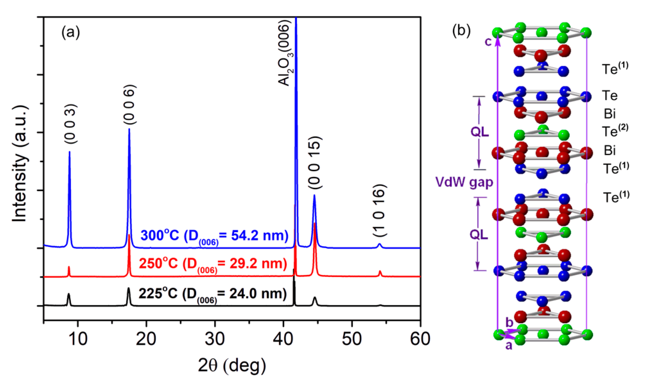
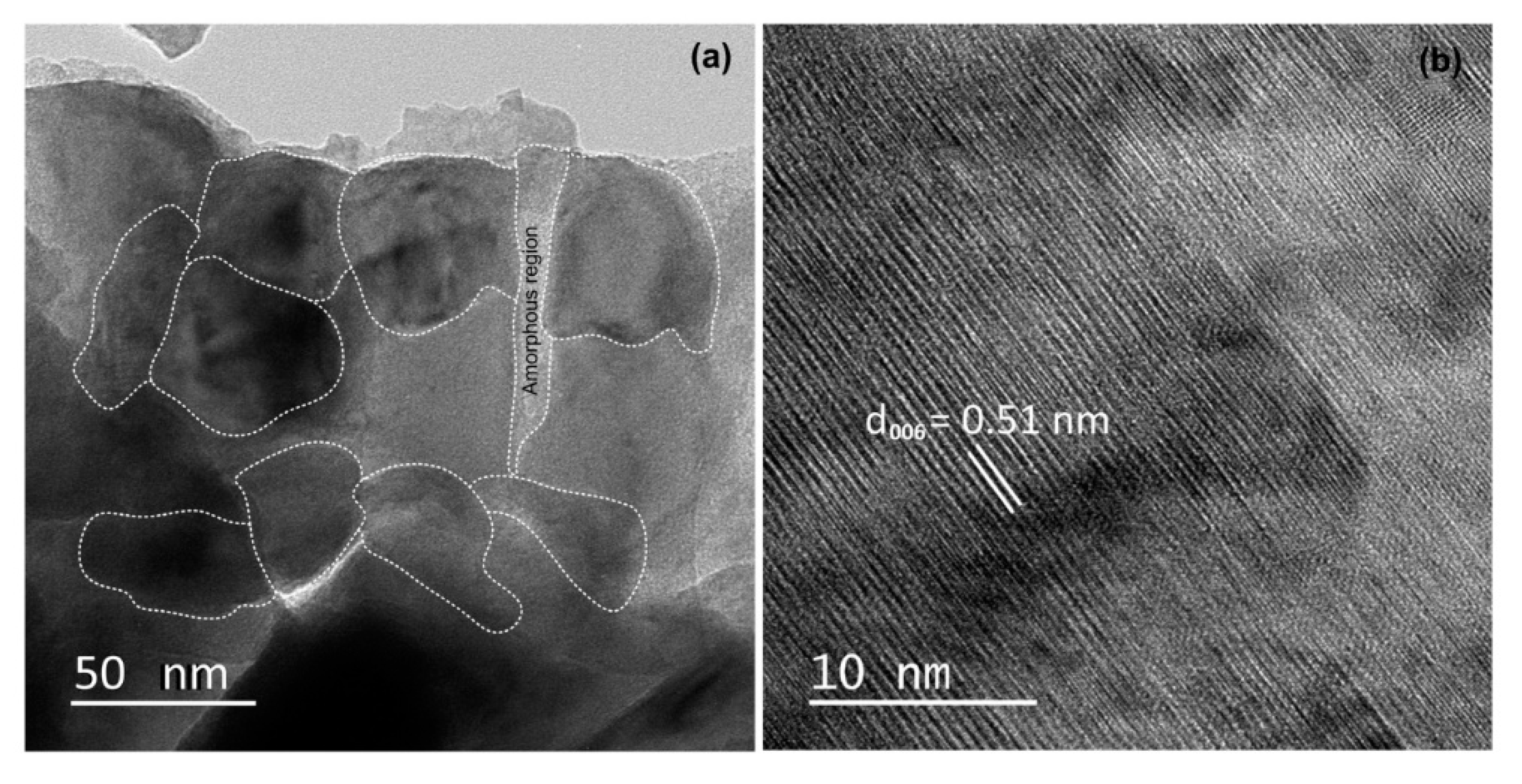
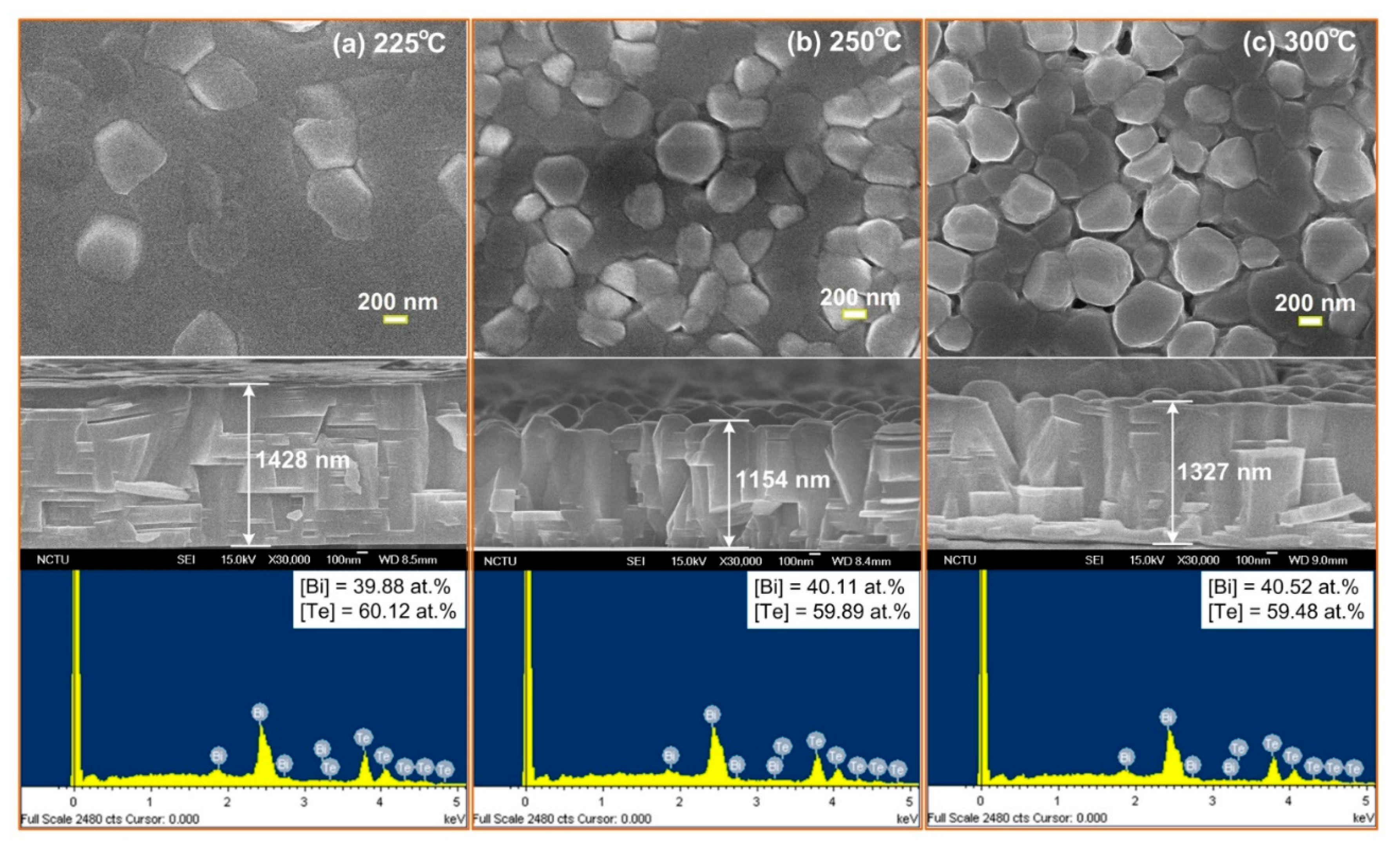
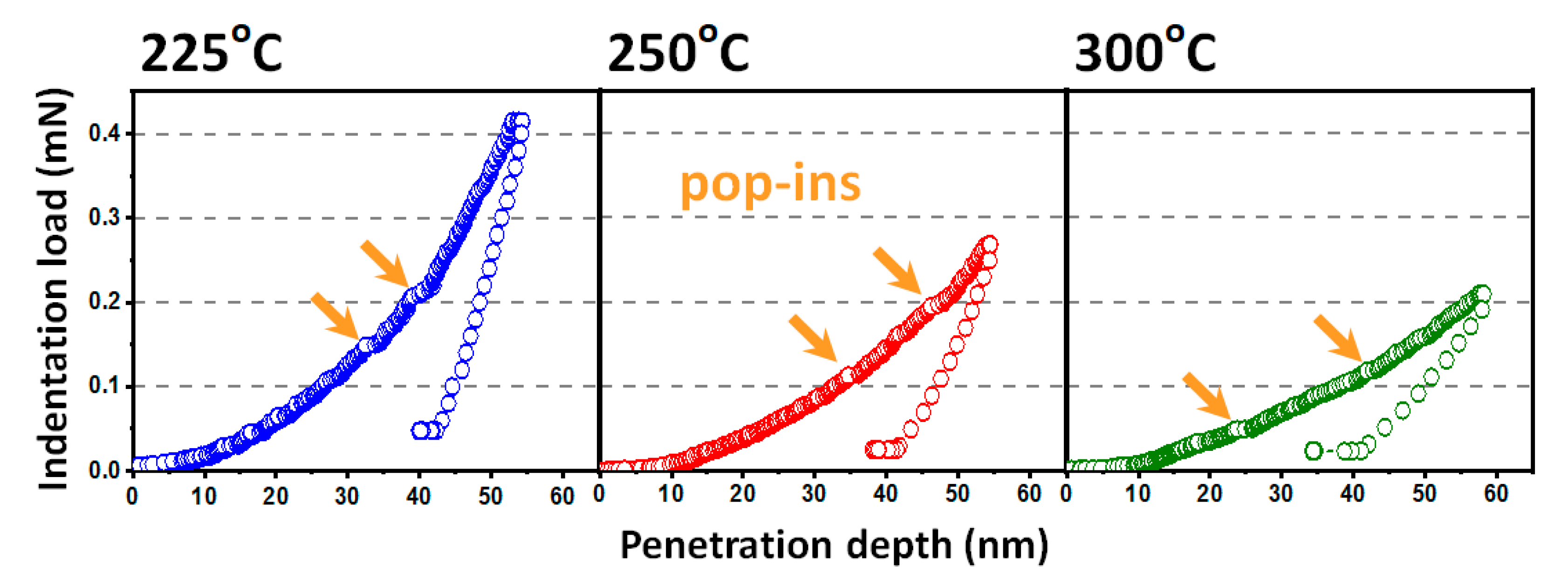
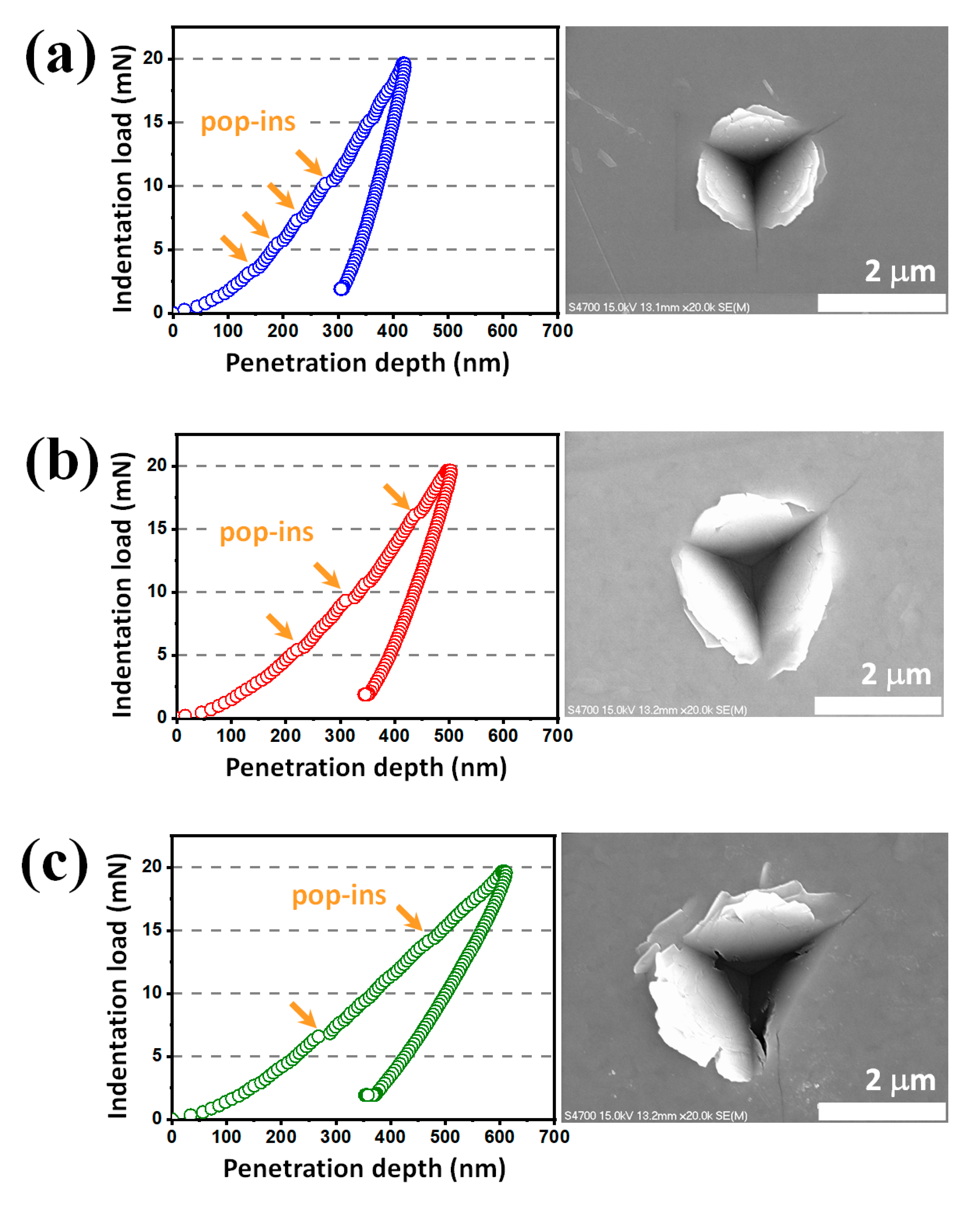
3. Results and Discussion

Figure 1a shows the XRD patterns of films, which can be unambiguously indexed as (003), (006), and (0015) of the rhombohedral Bi2Te3 phase (JCPDS card No. 82-0358). It is worth noting that the intensity ratios between the (0 0 6) and (1 0 16) diffraction peaks were 6.7, 7.8, and 20.2 for films deposited at 225 °C, 250 °C, and 300 °C, respectively, which were all substantially higher than the value of 1 obtained from the standard powder diffraction data file (JCPDS card No. 82-0358), confirming the highly (00l)-oriented characteristic of the present Bi2Te3 films. In addition, the preferred in-plane orientation was not found by the XRD phi-scan. Therefore, the Bi2Te3 films are polycrystalline and highly c-axis-oriented (or textured films). Noticeably, the crystal structure of Bi2Te3 is rhombohedral with a space group D 3 d 5 ( R 3 ¯ m ), which can be represented by a hexagonal primitive cell consisting of three quintuple-layers (QL). Each QL is about 1 nm-thick with 5-atomic-layer stacking in sequence, namely –(Te(1)–Bi–Te(2)–Bi–Te(1))–, along the c-axis, as depicted schematically in Figure 1b. The bonding between the QLs is the Van der Waals (VdW) Te(1)–Te(1) bond, which is significantly weaker than the ionic–covalent Bi-Te bonds within the QLs [6,18].
It is also evident from Figure 1a that the diffraction peaks exhibit higher intensity and narrower width with increasing TS, indicating that the crystallinity of the films is progressively improved when TS increases. We used Scherrer’s formula [19], Ds = 0.9λ/(βcosθ), to estimate the crystallite size (Ds) of the Bi2Te3 thin films, wherein λ, β, and θ are the X-ray wavelength, the full-width-at-half-maximum (FWHM) of the selected diffraction peak, and the corresponding Bragg diffraction angle, respectively. Here, we chose the (006) peak to calculate crystallite sizes, and the sizes are 24.0 nm, 29.2 nm, and 54.2 nm for the films deposited at TS of 225 °C, 250 °C, and 300 °C, respectively. These results clearly indicate that TS imposes a marked effect on the crystallite size. This observation can be understood as the following. At a lower TS, due to the higher extent of supersaturation and the lower surface diffusion rate, the reduced critical size and the nucleation energy barrier for the nuclei are reduced, which leads to an increased number of nucleation sites and an eventually smaller grain size [6].
Furthermore, by using the Williamson—Hall (WH) equation [20,21], the effects of the crystalline size-induced broadening and strain-induced broadening of XRD results for the Bi2Te3 thin films at various TS can be determined. The WH equation is as follows:
βcosθ = (0.9λ/DWH) + 4ε·sinθ
where ε is the microstrain. The WH equation represents a straight line between 4sinθ (X-axis) and βcosθ (Y-axis). The slope of the line gives the value of the microstrain. Both the crystalline size (DWH) and microstrain (ε) contribute to the broadening of the XRD spectra of the Bi2Te3 thin films and are listed in Table 1. It is noted that the incorporation of the microstrain effect is attributed to the different values of the crystalline size significantly. The values of the crystalline size of the TS-treated Bi2Te3 thin films calculated using Scherrer’s equation are noticeably smaller than those calculated using the WH equation that gave rise to the influence of the microstrain on the XRD results. Furthermore, both the values of Ds and DWH are enlarged, indicating that the overall crystallinity of the Bi2Te3 thin films was remarkably improved by the increased TS. The ε increases monotonically from 0.21% to 0.29% with increasing TS from 225 °C to 300 °C, which can be attributed to the newly created interfaces associated with the TS-dependent crystallite size and evolving grain shapes.
Figure 2a shows a low-magnification TEM image Bi2Te3 film deposited at the TS of 300 °C, in which some crystallites are presented by the dotted areas. It can be seen that the crystallite sizes are approximately 50–60 nm, agreeing well with the estimated crystallite size obtained from the XRD results. Moreover, an HRTEM image of a crystallite clearly presents the projected periods of 0.51 nm along the c-axis (Figure 2b), which corresponds to the lattice spacing of the Bi2Te3 (006) planes. These TEM results are further confirmed by the crystallite sizes and gain insight into the crystal structure of the textured Bi2Te3 films in this study.
Figure 3 depicts the SEM photographs, revealing the surface morphology of the Bi2Te3 films grown at different TS from 225 to 300 °C. The SEM images show that all films exhibit the typical polygonal granular morphology of a polycrystalline microstructure, and the grain size increases with increasing TS. This result is in line with the TS-dependent crystallite size tendency obtained from the XRD results (Figure 1). It is noted that the grain size observed from the SEM images shown in Figure 3 appears to be larger than the crystallite size estimated using the XRD data or observed directly from the HRTEM images because a “grain” in the SEM image may be composed of agglomerated grains and/or even include amorphous regions [24]. In addition, the EDS results confirm that all films have stoichiometry very close to that of the Bi2Te3 phase, which is necessary for obtaining the pure Bi2Te3 phase for all the investigated films. Noticeably, the Te composition reduces slightly from 60.12 at.% for the 225 °C film to 59.48 at.% for the 300 °C film. This could be due to the re-evaporation of Te from the heated substrates being much faster than that of Bi at elevated temperatures. The cross-sectional SEM images in Figure 3 show that the films had a thickness in the 1154–1428 nm range and layered structures.
As discussed above, the TS evidently showed significant effects on the film microstructures. The next prominent question is how it affects the nanomechanical properties of the films. Figure 4 shows the typical load—depth curves (Ph-curves) obtained from the nanoindentation CSM measurements on the Bi2Te3 films at various TS of 225 °C, 250 °C, and 300 °C. We kept the total penetration depth to within approximately 55 nm, which is well below the 30% criterion (film thickness of 1154–1428 nm) suggested by Li et al. [25], in which the indentation depth should never exceed 30% of the films’ thickness or the dimension of the nanostructures to avoid any complications from the substrate.
The hardness and Young’s modulus of the Bi2Te3 thin films are directly determined by the Ph-curves obtained from CSM measurements following the Oliver and Pharr method [17]. The results are shown in Figure 5. Briefly, the values of hardness (H) of the Bi2Te3 films are 5.2 ± 0.3, 4.0 ± 0.1, and 3.4 ± 0.2 GPa for the films deposited at 225 °C, 250 °C, and 300 °C, respectively. Similarly, the values of Young’s modulus (Ef) are 125.2 ± 6.9, 98.3 ± 2.1, and 62.5 ± 1.4 GPa for the Bi2Te3 films grown at 225 °C, 250 °C, and 300 °C, respectively. This means that both the values of H and Ef of the Bi2Te3 thin films monotonically decrease with increasing TS. Noticeably, the H and Ef of the present Bi2Te3 thin films are significantly larger than that reported for the bulk Bi2Te3 (H = 1.6 ± 0.2 GPa and E = 32.4 ± 2.9 GPa) [22]. The reason for the apparent discrepancy is not clear at present. Nevertheless, by comparing the results of the films in this study with that reported in Ref. [23], the stoichiometric levels and crystallite orientation of the films may have intimate correlations with the H and Ef results. We found that the H and Ef values of the close stoichiomectric Bi2Te3 films grown using the Bi2Te8 target are significantly larger than those of the Te-deficient Bi2Te3 films grown using the Bi2Te3 target [23]. Similar behaviors have also been reported in the Bi2Se3 thin films [26]. Notably, for the present Bi2Te3 films, the intensity of the (006)-diffraction peak is dominantly higher than that of the (0015)-diffraction peak, whereas the Bi2Te3 films in Ref. [23] showed reversed behavior for the intensity of the two peaks, presumably due to the different experimental conditions. We found that the mechanical properties of the PLD-grown Bi2Te3 films on the Al2O3 (001) substrates substantially were enhanced when they were grown using a Te-rich target (e.g., Bi2Te8) under a relatively high helium gas (e.g., 200 mTorr) pressure and at a moderately low TS (e.g., 225 °C). Additionally, compared with the previous studies [22,23], the structural and mechanical properties of the Bi2Te3 thin films are listed in Table 1.
On the other hand, as displayed in the inset of Figure 5, the hardness of the films as a function of the crystallite size can be described satisfactorily by the empirical Hall—Petch relation [27], where H(DWH) = H0 + k D WH 1 / 2 (H0 is the lattice friction stress and k is the Hall-Petch constant). The fitting yields   H ( D WH ) = 24.7 D WH 1 / 2 + 0.2 . Since the dislocation motion is recognized to play the primary role in giving rise to the phenomena describable by the Hall—Petch relation, it can also explain the pop-ins in the Ph-curves for the Bi2Te3 thin films by linking the observed pop-ins event to the abrupt plastic flow associated with the massive dislocation activities during nanoindentation (as shown in Figure 4). As is evident from the above results, higher TS apparently has led to a microstructure with larger crystallite size and better crystallinity for the Bi2Te3 thin films associated with the increased TS that could reduce the capability of hindering the dislocation movement, hence leading to decreases in the H and Ef values.
As indicated by the arrows shown in Figure 4 and Figure 6, along the loading segment of the Ph-curves, clear discontinuities reflecting the pop-ins phenomena are observed. Such behavior, in fact, has been ubiquitously observed in single crystal [22] and thin films [23] of Bi2Te3, when similar nanoindentation tests were undertaken. The fact that it occurs in a vast variety of loading segments associated with a wide range of corresponding strain rates during the test indicates that the phenomena, especially the first pop-in event, are not activated thermally. Instead, the phenomena are often explained in terms of dislocation nucleation and/or propagation [28,29], or development of induced micro-cracks [30,31] during nanoindentation. The possibility of a phase pressure-induced transition, however, can be ruled out. Due to the in situ high pressure XRD experiments carried out on Bi2Te3 [32,33,34], the magnitude of the applied pressure required to induce the phase transitions is orders of magnitude higher than the apparent room-temperature hardness obtained for the present Bi2Te3 films. Moreover, the absence of “pop-out” discontinuities along the unloading segment of the Ph-curves (Figure 4 and Figure 6) also support that, unlike that observed in nanoindented Si [35,36], the phase transition is not involved here. Consequently, we believe that the predominant deformation mechanism prevailing in the present case must mainly associate with the nucleation and subsequent propagation of dislocations.
For the context of the dislocation activity-mediated scenario, the first “pop-in” event can be attributed to the transition of deformation behaviors. Namely, the pop-in is the onset of plasticity, reflecting the indentation load at which the system switches from elastic to plastic deformation due to the movement of dislocations. Based on the above discussion, one can further calculate the corresponding critical shear stress (τc), at which the dislocation movement is initiated using the following equation: τ c = ( 0.31 / π ) [ 6 P c ( E r / R ) 2 ] 1 / 3   [37], where Pc is the load at which the load-depth discontinuity occurs, R is the radius of the tip of nanoindenter, and E r is the reduced elastic modulus defined in the Materials and Method section. The obtained values for τc are approximately 2.2, 1.4, and 1.0 GPa for the Bi2Te3 films deposited at the TS of 225, 250, and 300 °C, respectively. Alternatively, τc may also be regarded as the stress responsible for massive homogeneous nucleation of the dislocations within the region deformed underneath the tip.
Figure 6 shows the phenomena of Berkovich nanoindentation-induced cracking and the pile-up along the corners and edges of the residual indent clearly. Fracture toughness (Kc) is another prominent mechanical property of materials in nanoindentation, which can be determined by [38] K c = α · ( P m / c 3 / 2 ) · ( E f / H ) 1 / 2 , where α is an empirical constant depending solely on the geometry of the indenter, which is taken to be 0.016 for the Berkovich indenter, and c is the trace length of the radial crack appearing on the material surface at a maximum indentation loading (Pm) of 20 mN. The Kc values of the Bi2Te3 thin films thus obtained are 1.42, 1.21, and 0.88 MPa·m1/2 for films deposited at the TS of 225 °C, 250 °C, and 300 °C, respectively. Moreover, the fracture energy (Gc) of the Bi2Te3 thin films is estimated based on the elastic modulus and fracture toughness using the equation [39] G c = K c 2 · ( 1 ν 2 / E f ) , where the Gc values of the Bi2Te3 thin films are 0.15, 0.14, and 0.12 Jm−2 for the films deposited at the TS of 225 °C, 250 °C, and 300 °C, respectively. The values of Kc and Gc of the Bi2Te3 thin films are also listed in Table 1. Accordingly, as is evident from the SEM photographs shown in Figure 3, the cracks propagate in a straight line and exhibit a trans-granular cracking behavior, which confirms that the grain boundaries have effectively obstructed the inter-granular crack propagation.
It is worth noting that the Bi2Te3 film grown at the TS of 225 °C can be considered the optimal film because of its excellent mechanical properties of H = 5.2 ± 0.3 GPa and Ef = 125.2 ± 6.9 GPa for thermoelectric applications [40].

4. Conclusions

In summary, the Bi2Te3 thin films were grown on c-plane sapphire substrates at various TS from 225 to 300 °C under a helium ambient pressure of 200 mTorr using a Bi2Te8 target. The TS dependence of the structural, morphological, compositional, and nanomechanical properties of the Bi2Te3 films was systematically studied using XRD, TEM, SEM, EDS, and nanoindentation methods. As a result, all the films exhibited the Bi2Te3 phase, highly c-axis preferred orientation, granular morphology, and good stoichiometry. Moreover, the crystallite size of the films monotonically increased with increasing TS from 225 to 300 °C. The hardness (Young’s modulus) of the Bi2Te3 thin films decreased from 5.2 GPa (125.2 GPa) to 3.4 GPa (62.5 GPa) when TS increased from 225 to 300 °C. The TS-dependent hardness and Young’s modulus is associated with the variation in crystallite size, which can be explained by the dislocation-mediated mechanism underlying the Hall—Petch relation. The calculated values of Kc and Gc of the Bi2Te3 thin films were in the ranges of 0.88–1.42 MPa·m1/2 and 0.12–0.15 Jm−2, and their values were systematically decreased with increasing TS.

Author Contributions

H.-P.C., P.H.L., L.T.C.T. and Y.-C.C. contributed to the experiments and analyses. P.H.L., L.T.C.T., S.-R.J., I.-J.T., C.-M.L. and J.-Y.J. contributed to the discussion on materials characterizations. P.H.L., L.T.C.T., S.-R.J. and J.-Y.J. designed the project of experiments and drafted the manuscript. All authors have read and agreed to the published version of the manuscript.

Funding

The research was funded by the Ministry of Science and Technology, Taiwan, under Contract Nos. MOST 110-2221-E-214-013, MOST 109-2112-M-009-014-MY2, and Vietnam National Foundation for Science and Technology Development (NAFOSTED) under Grant No. 103.02-2019.374.

Institutional Review Board Statement

Not applicable.

Informed Consent Statement

Not applicable.

Data Availability Statement

Not applicable.

Acknowledgments

We acknowledge the support of time and facilities from Can Tho University of Medicine and Pharmacy for this study, and thank the MANALAB at ISU.

Conflicts of Interest

The authors declare no conflict of interest.

References

  1. Luo, X.; Sullivan, M.B.; Quek, S.Y. First-principles investigations of the atomic, electronic, and thermoelectric properties of equilibrium and strained Bi2Se3 and Bi2Te3 including van der Waals interactions. Phys. Rev. B 2012, 86, 184111. [Google Scholar] [CrossRef] [Green Version]
  2. Rowe, D.M. CRC Handbook of Thermoelectrics; CRC Press Inc.: New York, NY, USA, 1995. [Google Scholar]
  3. Mansoor, M.A.; Ismail, A.; Yahya, R.; Arifin, Z.; Tiekink, E.R.T.; Weng, N.S.; Mazhar, M.; Esmaeili, A.R. Perovskite-structured PbTiO3 thin films grown from a single-source precursor. Inorg. Chem. 2013, 52, 5624–5626. [Google Scholar]
  4. Munawar, K.; Mansoor, M.A.; Olmstead, M.M.; Zaharinie, T.; Zubir, M.N.M.; Haniffa, M.; Wan Jefrey Basirun, W.J.; Mazhar, M. Fabrication of Ag–ZnO composite thin films for plasmonic enhanced water splitting. Mater. Chem. Phys. 2020, 255, 123220. [Google Scholar] [CrossRef]
  5. Liaqat, R.; Mansoor, M.A.; Iqbal, J.; Jilani, A.; Shakir, S.; Kalam, A.; Wageh, S. Fabrication of metal (Cu and Cr) incorporated nickel oxide films for electrochemical oxidation of methanol. Crystals 2021, 11, 1398. [Google Scholar] [CrossRef]
  6. Le, P.H.; Liao, C.-N.; Luo, C.W.; Leu, J. Thermoelectric properties of nanostructured bismuth–telluride thin films grown using pulsed laser deposition. J. Alloys Compd. 2014, 615, 546–552. [Google Scholar] [CrossRef]
  7. Nandihalli, N. Thermoelectric films and periodic structures and spin Seebeck effect systems: Facets of performance optimization. Mater. Today Energy 2022, 25, 100965. [Google Scholar] [CrossRef]
  8. Nandihalli, N.; Liu, C.-J.; Mori, T. Polymer based thermoelectric nanocomposite materials and devices: Fabrication and characteristics. Nano Energy 2020, 78, 105186. [Google Scholar] [CrossRef]
  9. Bao, L.H.; Xu, Z.H.; Li, R.; Li, X.D. Catalyst-free synthesis and structural and mechanical characterization of single crystalline Ca2B2O5·H2O nanobelts and stacking faulted Ca2B2O5 nanogrooves. Nano Lett. 2010, 10, 255–262. [Google Scholar] [CrossRef]
  10. Sun, Y.; Liu, J.; Blom, D.; Koley, G.; Duan, Z.; Wang, G.; Li, X.D. Atomic-scale imaging correlation on the deformation and sensing mechanisms of SnO2 nanowire. Appl. Phys. Lett. 2014, 105, 243105. [Google Scholar] [CrossRef]
  11. Jiang, T.; Khabaz, F.; Marne, A.; Wu, C.; Gearba, R.; Bodepudi, R.; Bonnecaze, R.T.; Liechti, K.M.; Korgel, B.A. Mechanical properties of hydrogenated amorphous silicon (a-Si:H) particles. J. Appl. Phys. 2019, 126, 204303. [Google Scholar] [CrossRef]
  12. Wiatrowski, A.; Obstarczyk, A.; Mazur, M.; Kaczmarek, D.; Wojcieszak, D. Characterization of HfO2 optical coatings deposited by mf magnetron sputtering. Coatings 2019, 9, 106. [Google Scholar] [CrossRef] [Green Version]
  13. Wang, S.H.; Jian, S.R.; Chen, G.J.; Cheng, H.Z.; Juang, J.Y. Annealing-driven microstructural evolution and its effects on the surface and nanomechanical properties of Cu-doped NiO thin films. Coatings 2019, 9, 107. [Google Scholar] [CrossRef] [Green Version]
  14. Bayansal, F.; Şahin, O.; Ҫetinkara, H.A. Mechanical and structural properties of Li-doped CuO thin films deposited by the successive ionic layer adsorption and reaction method. Thin Solid Films 2020, 697, 137839. [Google Scholar] [CrossRef]
  15. Li, X.D.; Bhushan, B. A review of nanoindentation continuous stiffness measurement technique and its applications. Mater. Charact. 2002, 48, 11–36. [Google Scholar] [CrossRef]
  16. Sneddon, I.N. The relation between load and penetration in the axisymmetric boussinesq problem for a punch of arbitrary profile. Int. J. Eng. Sci. 1965, 3, 47–57. [Google Scholar] [CrossRef]
  17. Oliver, W.C.; Pharr, G.M. An improved technique for determining hardness and elastic modulus using load and displacement sensing indentation experiments. J. Mater. Res. 1992, 7, 1564–1583. [Google Scholar] [CrossRef]
  18. Chen, Y.L.; Analytis, J.G.; Chu, J.H.; Liu, Z.K.; Mo, S.K.; Qi, X.L.; Zhang, H.J.; Lu, D.H.; Dai, X.; Fang, Z.; et al. Experimental realization of a three-dimensional topological insulator, Bi2Te3. Science 2009, 325, 178–181. [Google Scholar] [CrossRef] [Green Version]
  19. Cullity, B.D.; Stock, S.R. Element of X-ray Diffraction; Prentice Hall: Upper Saddle River, NJ, USA, 2001; p. 170. [Google Scholar]
  20. Goh, K.H.; Haseeb, A.S.M.A.; Wong, Y.H. Effect of oxidation temperature on physical and electrical properties of Sm2O3 thin-film gate oxide on Si substrate. J. Electron. Mater. 2016, 45, 5302–5312. [Google Scholar] [CrossRef]
  21. Venkatewarlu, K.; Bose, A.C.; Rameshbabu, N. X-ray peak broadening studies of nanocrystalline hydroxyapatite by Williamson–Hall analysis. Physica B 2010, 405, 4256–4261. [Google Scholar] [CrossRef]
  22. Lamuta, C.; Cupolillo, A.; Politano, A.; Aliev, Z.S.; Babanly, M.B.; Chulkov, E.V.; Alfano, M.; Pagnotta, L. Nanoindentation of single-crystal Bi2Te3 topological insulators grown with the Bridgman–Stockbarger method. Phys. Status Solidi B 2016, 253, 1082–1086. [Google Scholar] [CrossRef]
  23. Tsai, C.H.; Tseng, Y.C.; Jian, S.R.; Liao, Y.Y.; Lin, C.M.; Yang, P.F.; Chen, D.L.; Chen, H.J.; Luo, C.W.; Juang, J.Y. Nanomechanical properties of Bi2Te3 thin films by nanoindentation. J. Alloys Compd. 2015, 619, 834–838. [Google Scholar]
  24. Tuyen, L.T.C.; Jian, S.R.; Tien, N.T.; Le, P.H. Nanomechanical and material properties of fluorine-doped tin oxide thin films prepared by ultrasonic spray pyrolysis: Effects of F-doping. Materials 2019, 12, 1665. [Google Scholar] [CrossRef] [PubMed] [Green Version]
  25. Li, X.D.; Gao, H.S.; Murphy, C.J.; Gou, L.F. Nanoindentation of Cu2O nanocubes. Nano Lett. 2004, 4, 1903. [Google Scholar] [CrossRef]
  26. Hwang, Y.M.; Pan, C.T.; Le, P.H.; Uyen, N.N.; Tuyen, L.T.C.; Nguyen, V.; Luo, C.W.; Juang, J.Y.; Leu, J.; Jian, S.R. Effects of stoichiometry on structural, morphological and nanomechanical properties of Bi2Se3 thin films deposited on InP(111) substrates by pulsed laser deposition. Coatings 2020, 10, 958. [Google Scholar] [CrossRef]
  27. Greer, J.R.; De Hosson, J.T.M. Plasticity in small-sized metallic systems: Intrinsic versus extrinsic size effect. Prog. Mater. Sci. 2011, 56, 654–724. [Google Scholar] [CrossRef]
  28. Jian, S.R.; Juang, J.Y.; Lai, Y.S. Cross-sectional transmission electron microscopy observations of structural damage in Al0.16Ga0.84N thin film under contact loading. J. Appl. Phys. 2008, 103, 033503. [Google Scholar] [CrossRef] [Green Version]
  29. Jian, S.R. Cathodoluminescence rosettes in c-plane GaN films under Berkovich nanoindentation. Opt. Mater. 2013, 35, 2707–2709. [Google Scholar] [CrossRef]
  30. Yen, C.Y.; Jian, S.R.; Lai, Y.S.; Yang, P.F.; Liao, Y.Y.; Jang, J.S.C.; Lin, T.H.; Juang, J.Y. Mechanical properties of the hexagonal HoMnO3 thin films by nanoindentation. J. Alloys Compd. 2010, 508, 523–527. [Google Scholar] [CrossRef]
  31. Smolik, J.; Kacprzyńska-Gołacka, J.; Sowa, S.; Piasek, A. The analysis of resistance to brittle cracking of tungsten doped TiB2 coatings obtained by magnetron sputtering. Coatings 2020, 10, 807. [Google Scholar] [CrossRef]
  32. Zhu, L.; Wang, H.; Wang, Y.; Lv, J.; Ma, Y.; Cui, Q.; Ma, Y.; Zou, G. Substitutional alloy of Bi and Te at high pressure. Phys. Rev. Lett. 2011, 106, 145501. [Google Scholar] [CrossRef]
  33. Einaga, M.; Ohmura, A.; Nakayama, A.; Ishikawa, F.; Yamada, Y.; Nakano, S. Pressure-induced phase transition of Bi2Te3 to a bcc structure. Phys. Rev. B 2011, 83, 092102. [Google Scholar] [CrossRef] [Green Version]
  34. Manjón, F.J.; Vilaplana, R.; Gomis, O.; Pérez-González, E.; Santamaría-Pérez, D.; Marín-Borrás, V.; Segura, A.; González, J.; Rodríguez-Hernández, P.; Muñoz, A.; et al. High-pressure studies of topological insulators Bi2Se3, Bi2Te3, and Sb2Te3. Phys. Status Solidi B 2013, 250, 669–676. [Google Scholar] [CrossRef]
  35. Bradby, J.E.; Williams, J.S.; Wong-Leung, J.; Swain, M.V.; Munroe, P. Transmission electron microscopy observation of deformation microstructure under spherical indentation in silicon. Appl. Phys. Lett. 2000, 77, 3749. [Google Scholar] [CrossRef]
  36. Jian, S.R.; Chen, G.J.; Juang, J.Y. Nanoindentation-induced phase transformation in (1 1 0)-oriented Si single-crystals. Curr. Opin. Solid State Mater. Sci. 2010, 14, 69–74. [Google Scholar] [CrossRef]
  37. Johnson, K.L. Contact Mechanics; Cambridge University Press: Cambridge, UK, 1985. [Google Scholar]
  38. Casellas, D.; Caro, J.; Molas, S.; Prado, J.M.; Valls, I. Fracture toughness of carbides in tool steels evaluated by nanoindentation. Acta Mater. 2007, 55, 4277–4286. [Google Scholar] [CrossRef]
  39. Rafiee, M.A.; Rafiee, J.; Srivastava, I.; Wang, Z.; Song, H.; Yu, Z.Z.; Koratkar, N. Fracture and Fatigue in Graphene Nanocomposites. Small 2010, 6, 179–183. [Google Scholar] [CrossRef]
  40. Le, P.H.; Liao, C.N.; Luo, C.W.; Lin, J.Y.; Leu, J. Thermoelectric properties of bismuth-selenide films with controlled morphology and texture grown using pulsed laser deposition. Appl. Surf. Sci. 2013, 285, 657–663. [Google Scholar] [CrossRef]
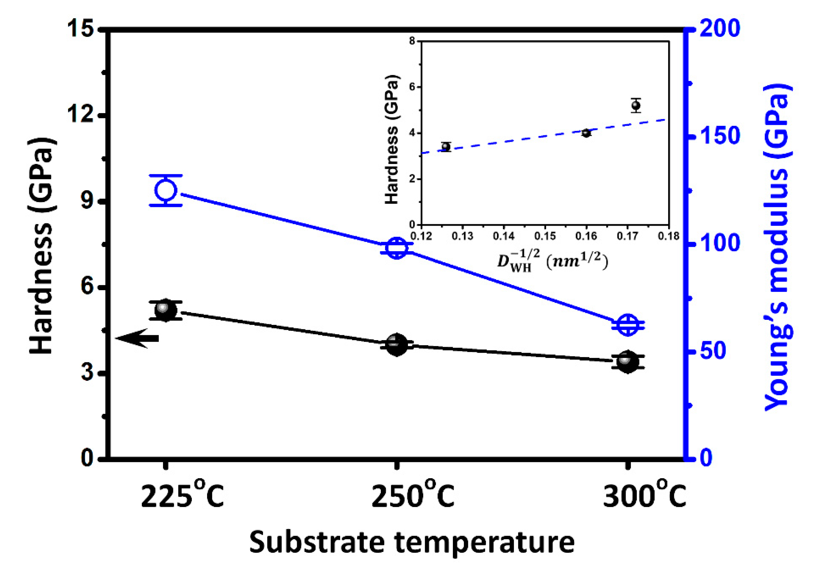
Figure 1. (a) XRD patterns of the Bi2Te3 thin films deposited on the c-plane sapphire substrates at the various TS of 225 °C, 250 °C, and 300 °C, respectively. D(006) is the calculated grain size of the films using the Scherrer equation and Bi2Te3 (006) peaks. (b) The schematics depicts the crystal structure of Bi2Te3.
Coatings 12 00871 g001
Figure 2. TEM images of the Bi2Te3 film deposited at the TS of 300 °C. The dotted areas in (a) are used to guide the eyes of some crystallites; (b) the magnified HRTEM image obtained from (a).
Coatings 12 00871 g002
Figure 3. SEM images (upper: top view and middle: cross section) and EDS spectra of the Bi2Te3 thin films deposited at various substrate temperatures of 225, 250, and 300 °C.
Coatings 12 00871 g003
Figure 4. CSM nanoindentation Ph-curves of the Bi2Te3 thin films deposited on the c-plane sapphire substrates at the various TS from 225 to 300 °C.
Coatings 12 00871 g004
Figure 5. The hardness as a function of grain size for the Bi2Te3 thin films. The dash lines are the fitting using the Hall—Petch equation.
Coatings 12 00871 g005
Figure 6. Berkovich nanoindentation on the Bi2Te3 thin films at various TS: (a) 225 °C, (b) 250 °C, and (c) 300 °C. The corresponding SEM indentations are displayed to the right of the load-depth curves.
Coatings 12 00871 g006
Table 1. The structural and mechanical properties of the Bi2Te3 thin films.
Bi2Te3Ds
(nm)
DWH
(nm)
ε
(%)
H
(GPa)
Ef
(GPa)
τc (GPa)Kc (MPa·m1/2)Gc
(Jm−2)
Bulk [22]1.6 ± 0.232.4 ± 2.9
Thin films [23]
(helium gas pressure)
2 × 10⁻⁵–2 × 10⁻³ Torr
11–202.9–4.0106.3–127.50.9–1.3
Thin films [#]
TS = 225 °C
24.032.60.215.2 ± 0.3125.2 ± 6.92.21.420.15
Thin films [#]
TS = 250 °C
29.240.20.244.0 ± 0.198.3 ± 2.11.41.210.14
Thin films [#]
TS = 300 °C
54.262.70.293.4 ± 0.262.5 ± 1.41.00.880.12
[#]: this work.
Publisher’s Note: MDPI stays neutral with regard to jurisdictional claims in published maps and institutional affiliations.

