Article

Importance of Dielectric Elements for Attaining Process Uniformity in Capacitively Coupled Plasma Deposition Reactors

Department of Mechanical Engineering, Gachon University, Seongnam 13120, Korea
Coatings 2022, 12(4), 457; https://doi.org/10.3390/coatings12040457
Submission received: 27 February 2022 / Revised: 21 March 2022 / Accepted: 25 March 2022 / Published: 28 March 2022
(This article belongs to the Special Issue New Advances in Plasma Deposition and Its Applications)

Abstract

:
In this study, the effect of dielectric elements on plasma radial uniformity was analyzed for a 300 mm wafer process in a capacitively coupled plasma deposition reactor. Based on a two-dimensional self-consistent fluid model, numerical simulations were performed for SiH4/He discharges at 1200 Pa and at the radio frequency of 13.56 MHz. Although in current plasma processes the wafer is often coated with non-conducting films and placed on a ceramic substrate, related materials have not been analyzed. Therefore, the plasma characteristics were studied in depth by changing the wafer material from silicon to quartz, the electrode material from aluminum to aluminum nitride, and the sidewall material from quartz to perfect dielectric. It was demonstrated that dielectric elements with a lower dielectric constant modify the spatial distributions of plasma parameters. In spite of the thinness of the wafer, as the dielectric constant of the wafer decreases, the electric field at the wafer edge becomes weaker owing to the stronger surface-charging effect. This gives rise to the relatively lower density of reactive species such as SiH2+, Si+, He*, and SiH3 near the wafer edge. In addition, radially uniform plasma was induced by the perfect dielectric sidewall, regardless of the dielectric constant of the wafer. This modification occurred because the radial positions of the peak values of the plasma parameters were moved away from the wafer edge. Therefore, the uniform distribution of the plasma density could be largely achieved by the optimal combination of dielectric elements.

1. Introduction

Despite various efforts, technically complex issues such as the electron heating mechanism and the plasma distribution control have not been sufficiently resolved in the coating process using the capacitively coupled plasma (CCP) deposition reactors [1,2]. However, CCP deposition reactors have been widely adopted in the current semiconductor industry [3]. These CCP deposition reactors often need to be developed and modified to produce state-of-the-art microchips. As a result, it has become increasingly important to address the technical challenges associated with the realization of uniform deposition processes. The plasma density and the ion flux toward the wafer surface must be radially uniform and homogeneous to ensure consistent deposition or etching effectiveness on the entire wafer surface in today’s fabrication processes [4,5]. In addition, the ongoing shrinkage of devices also amplifies the need for obtaining uniform and homogeneous plasma near the wafer. Therefore, the control of the plasma uniformity is one of the major challenges recently designed plasma systems need to overcome [6,7].
Many factors affect the plasma uniformity simultaneously, which can be divided into three categories: the conditions of the source gas (e.g., the gas temperature and the gas pressure), the driving source (e.g., the radio frequency (RF), phase shift, pulsing, and input power), the reactor geometry (e.g., the shape, spacing, and radius of the electrode), and the material of the electrode (e.g., aluminum, aluminum oxide, and aluminum nitride). In CCP discharges, when electromagnetic phenomena such as the effects of standing waves are negligible, the plasma uniformity is determined by electrostatic phenomena such as the electrode edge effect [8,9]. Therefore, research related to plasma uniformity has mostly focused on ways in which to suppress the edge effect and to obtain homogeneous plasmas. In the previous studies, both numerically and experimentally, it has been shown that the edge effect could be effectively suppressed and plasma uniformity could be optimized by carefully controlling the temperature, velocity distribution, and composition of the gas, in addition to the inlet conditions, the electrode temperature, and the electrode spacing [10,11,12,13]. Focusing on the RF source control, Xu et al. were able to show that the phase shift effect could determine the uniformity of the plasma density distribution and the ion flux in CCP discharges [14].
As a practical solution, the use of dielectric materials also has important effects on the plasma uniformity. As a result, dielectric elements have been employed in the design of CCP reactors [15,16,17,18,19,20,21,22,23,24]. For example, Yang and Kushner adopted a graded conductivity electrode on which multiple layers of dielectrics were deposited [20]. In their numerical work, they succeeded in modifying the radial uniformity of the plasma and the ion flux in the sheath. Based on the argon (Ar) discharges, Dalvie et al. reported that modulating the plasma potential near the sidewall reduced the inhomogeneity of the ionization rate [21]. Based on a 2D fluid model, Bi et al. numerically demonstrated that surrounding the electrode with the dielectric material could be an effective approach to suppress the edge effect and to enhance the plasma uniformity [22]. Kim and Manousiouthakis could induce the ion bombardment to be more radially uniform by increasing the impedance of the dielectric elements such as the nonconducting wafer and the quartz sidewall [23]. Michna and Ellingboe proposed the use of multitile systems in which neighboring tiles are out of phase to ensure good deposition uniformity in plasma-enhanced chemical vapor deposition (PECVD) processes [24].
It is worth noting that, to account for the accumulation of ions and electrons on the surface of the dielectric, there is the so-called “surface-charging effect.” The relative permittivity of a dielectric element and its geometrical shape (i.e., its length and thickness) have an influence on how much charge accumulates on its surface and therefore how much potential is changed there [3]. This surface-charging effect leads to the formation of the opposite-direction electric field, which has an impact on the plasma behavior at the surface, especially on the uniformity of the plasma.
Despite its significant physical importance, however, previous systematic investigations of the dielectric elements on the plasma uniformity were limited to the use of simple chemistry or the application of plasma to etching. In this case, a noble gas such as Ar was considered, and the reactor conditions were simplified. An in-depth understanding of the effect of the dielectric elements on the plasma parameters in practical deposition reactors with gas mixtures has therefore become of great importance. The emphasis of this study is on the influence of the dielectric elements on the plasma uniformity in practical CCP PECVD. A mixture of SiH4 and He was selected for depositing amorphous hydrogenated silicon (a-Si:H) films. In the case study, simulations were performed in a cylindrical showerhead reactor adopted for processing 300 mm wafers. The plasma characteristics were systematically investigated by changing the wafer material from silicon (Si) to quartz (SiO2), the electrode material from aluminum (Al) to aluminum nitride (AlN), and the sidewall material from quartz (SiO2) to perfect dielectric. The computational model is briefly described in Section 2, results are presented in detail in Section 3, results are briefly discussed in Section 4, and a conclusion is provided in Section 5.

2. Materials and Methods

2.1. Governing Equations

Details of the governing equations of the self-consistent CCP model adopted here are explained in the previous publications [10,11,12,13,25]. Therefore, for brevity, only brief accounts of the equations are provided here. The electron energy balance is taken into account by solving:
( n e ε ) t + · [ 5 3 n e ε v e 5 3 n e D e ε ] = S ε .
Here, ne, ε, t, ve, De, and Sε are the electron density, the electron energy, the time, the electron velocity, the electron diffusion coefficient, and the source of the electron energy, respectively. The electron energy source, Sε, in Equation (1), is given by:
S ε = e J e · E n e i m s r ε r k r , i N i .
Here, −e, Je, E, kr,i, and Ni are the charge of an electron, the electron flux, the electric field, the rate coefficient of the rth reaction with the ith species, and the density of the ith species, respectively. Further, ms is the number of species involved in this reaction and εr represents the threshold energy in an inelastic collision or the mean electron energy loss in an elastic collision.
To obtain the electric potential ϕ, the Poisson equation is solved as given below:
2 ϕ = e ε 0 ( n p n e n q ) ,
where ε0 is the permittivity of free space, np is the positive ion density, and nq is the negative ion density.
The boundary condition for the dielectric surface is given as follows:
σ s t = e ( i q i J i , n J e , n ) ,
ε 0 E n ε d E d , n = σ s .
Here, σs, qi, Ji,n, Je,n, and εd are, respectively, the surface charge, the ion species charge unit, the flux of the ion species i, the flux of the electron, and the permittivity of the insulator. Note that subscript d represents the insulator.

2.2. Numerical Methods

The capacitively coupled SiH4/He plasma was simulated on the basis of a 2D fluid model using the commercial multiphysics software CFD-ACE+ (version 2020.5) [26]. A series of studies have successfully simulated SiH4/He discharge cases using CFD-ACE+, based on results from various previous studies [6,7,12,13]. The discretization of the electron density conservation and electron energy balance equation were calculated using the Scharfetter–Gummel exponential scheme. The electron impact reaction rates as well as the electron transport coefficients were calculated using CFD-ACE+. Simulated results obtained under different grid conditions were compared for grid independence. A total of 5598 nodes were used in this study because grid independence had been achieved since about 5000 nodes.

2.3. SiH4/He Plasma Chemistry

The deposition of a-Si:H films is often accomplished by diluting SiH4 with He to obtain the required film quality, and hence, a number of numerical and experimental studies concerning SiH4/He plasmas can be found in the literature [12,27,28,29]. For modeling SiH4/He plasmas, the neutral atom helium (He), the helium ion (He+), and the excited helium (He*, which represents excited helium atoms) were considered. There was detailed discussion in the previous publications of the chemical mechanisms that were used in this study and these mechanisms have been validated by reproducing the corresponding deposition rate profiles which match the experimental data [6,7,12,13].

3. Results

As depicted in Figure 1a, in its current configuration, the cylindrical CCP reactor has a top electrode (showerhead electrode) separated from the grounded reactor wall by a dielectric ring-shaped component. The inner surface of the dielectric ring plays the role of the sidewall. Voltage is applied to the top electrode at an RF of 13.56 MHz, whereas the bottom electrode is grounded. The bottom electrode is alternatively referred to as the heater in cases with nonisothermal boundary conditions because the wafer is often heated for process optimization. A silicon (Si, lossy dielectric; dielectric constant, k ≈ 12) or quartz (SiO2, nonconducting dielectric; dielectric constant, k ≈ 4) wafer is placed on top of the bottom electrode in cases in which placement of the wafer is considered. The wafer is surrounded by a Si or SiO2 ring (a so-called edge ring) to resolve the electrical discontinuity near the wafer edge.
Owing to its symmetrical construction, only half of the reactor is taken into account in the rz plane, where r is the radial coordinate and z is the axial coordinate. The right boundary interfaces with the dielectric sidewall, while the left boundary represents the symmetry axis. The source gases (SiH4/He) are fed into the reactor through a series of showerhead holes installed in the top electrode. After the process, the source gases are pumped out through the pump port at the bottom of the reactor. In this study, the mixture consisting of 50 sccm SiH4 and 5000 sccm He at 1200 Pa was used as the feed gas. As the amplitude of the potential Vrf was applied to the showerhead, the power delivered to the charged species equaled a preset value of 100 W. As depicted in the gas temperature contour in Figure 1a, the sidewall temperature (Tsw), the heater temperature (Th), and the showerhead temperature (Tsh) were set to 423, 673, and 473 K, respectively. Details of the seven cases considered in this study are listed in Table 1.
Note that in Figure 1b,c, the time-averaged He* production rate profile and density profile are depicted for Case 1 (the base case in Table 1). Despite the fact that the threshold energy of SiH4 ionization is considerably lower than that of He excitation or ionization, in the presence of the inlet condition (He dilution), the production of Si+ by dissociative excitation (He* quenching) is as important as the production of SiH2+ by direct impact ionization. The rate coefficients for the Si+ production were determined as shown below:
He* + SiH4 → Si+ + 2H + H2 + He + e, kr = 1.3 × 10⁻¹⁶ m3·s−1
where kr represents the reaction rate coefficient [30].

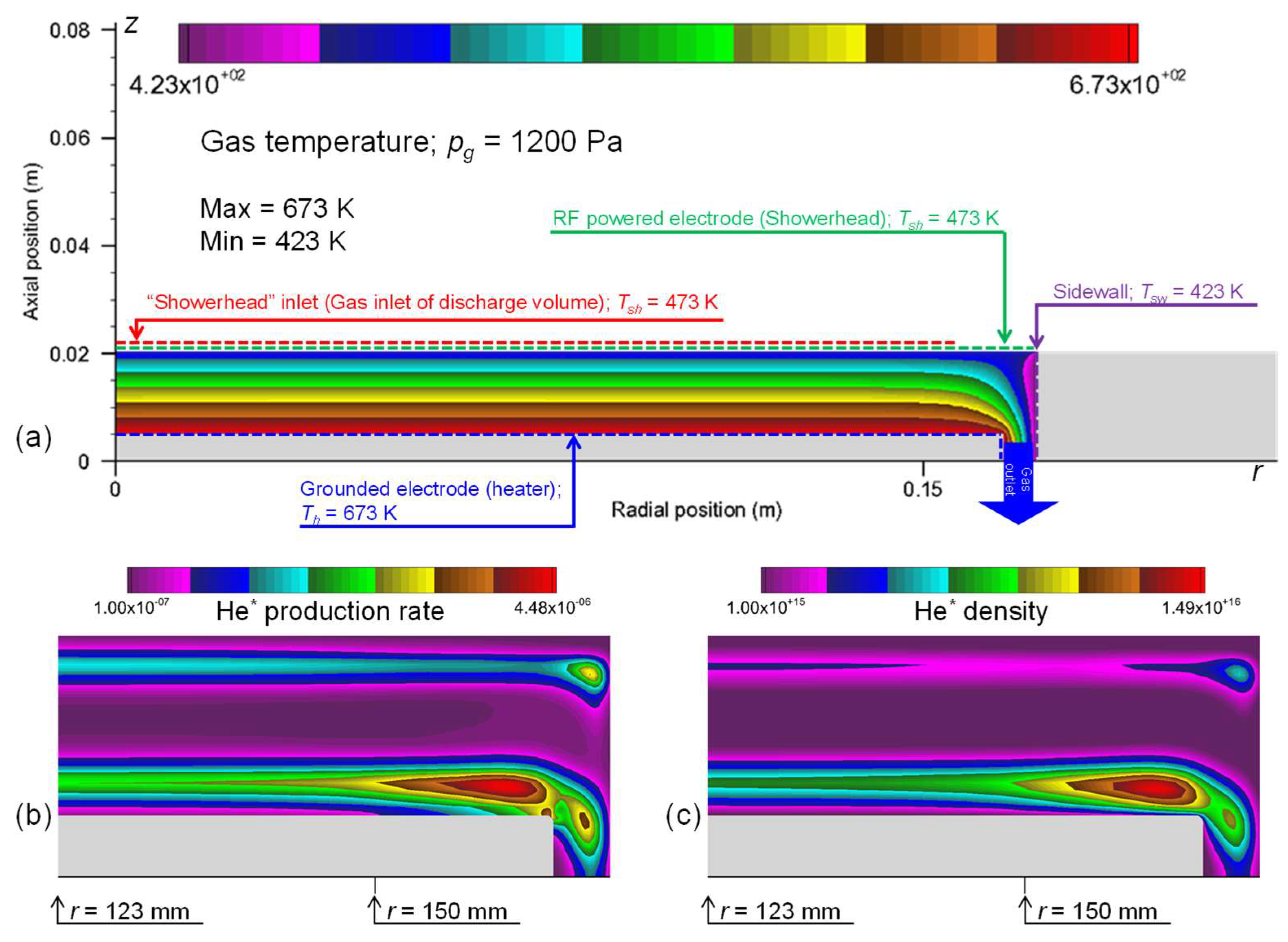
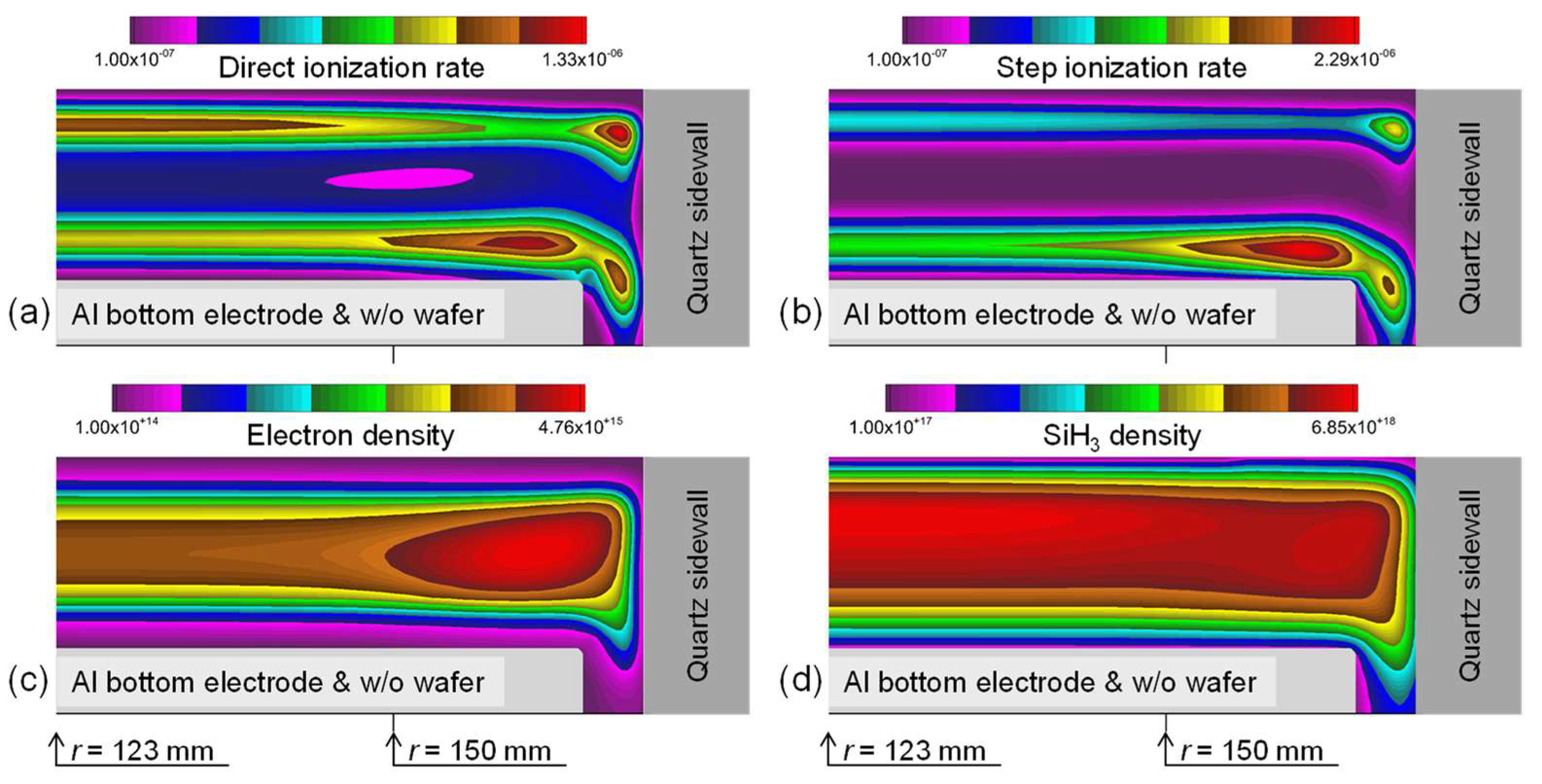
3.1. Analysis of the Base Case

The time-averaged simulation results for Case 1 (the base case with the quartz sidewall, the aluminum bottom electrode, and the absence of the dielectric wafer; see Table 1) are shown in Figure 2. Owing to the electrostatic effect, both the direct ionization rate (SiH2+ production) and the step ionization rate (Si+ production) are significantly enhanced near the edge of the bottom electrode, as depicted in Figure 2a,b. Therefore, the ionization rate profiles in the radial direction are highly nonuniform near the electrode edge: near the intersection of the axial and radial sheaths, ionization rates peak. The gradient of the electric potential causes this efficient ionization, as shown in Equation (2): in the heating term for the ionization, the electric field is determined by the gradient of the electric potential. Note that the ionization rates near the top and bottom sidewall are also highly nonuniform. Particularly, the ionization rates are highly focused around the top and bottom corners.
Figure 2c shows the time-averaged contours of the electron density, Ne (m−3). In Figure 2c, the off-axis maximum of the electron density (Neo) reaches 4.76 × 10¹⁵ (m−3). As shown in Figure 2d, the densities of SiH3 (m−3) (for Case 1) vary spatially. SiH3 was selected for analysis over a variety of other radicals and stable molecules due to its important role in the deposition of an a-Si:H film. Similar to the electron density profile, the SiH3 density profile also exhibits peak values near the edge of the bottom electrode. However, the difference is that the SiH3 density profile also has an on-axis maximum value owing to the transport phenomena.

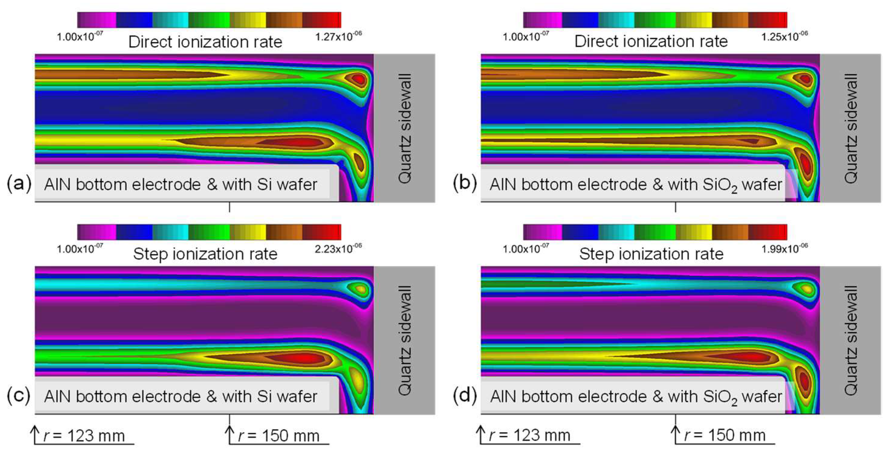
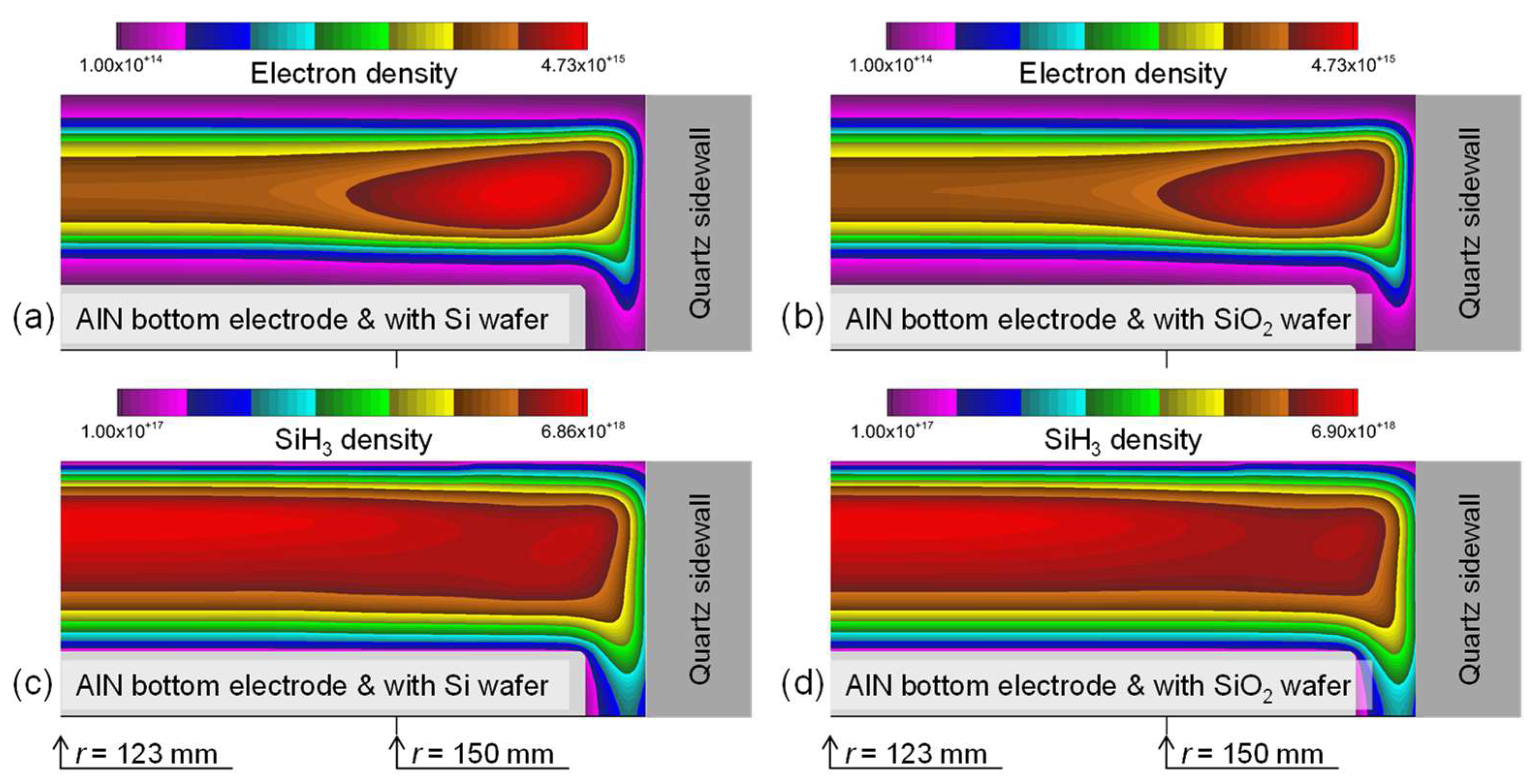
3.2. Effects of the Dielectric Wafer and the Dielectric Bottom Electrode

For the purpose of determining the effect of different electrical conditions on wafer surfaces, the conditions at the bottom of the reactor were changed in Cases 2 and 3 by placing the wafer on the bottom electrode. In Case 2, a Si (lossy dielectric, k ≈ 12) wafer was placed on the aluminum (grounded) bottom electrode, whereas in Case 3, a SiO2 (dielectric, k ≈ 4) wafer was placed on the aluminum (grounded) bottom electrode. In Cases 2 and 3, all the other conditions were identical to those of Case 1 (see Table 1). It should be noted that in many practical CCP processes, PECVD is often carried out with a bottom electrode manufactured from ceramic materials such as aluminum oxide (Al2O3) or aluminum nitride (AlN). Owing to their thermal robustness and low deformation rate, ceramic electrodes are often adopted in high-temperature processes to modulate the film quality by heating the wafer sufficiently. Therefore, for Case 4, the Si (lossy dielectric, k ≈ 12) wafer was placed on an AlN (dielectric, k ≈ 9) bottom electrode, whereas for Case 5, the SiO2 (dielectric, k ≈ 4) wafer was placed on an AlN (dielectric, k ≈ 9) bottom electrode. To ground the bottom electrode, on the bottom side of the wafer, the grounded boundary condition was applied. The other conditions of Cases 4 and 5 were the same as those of Cases 2 and 3 (See Table 1). For brevity, for Cases 2 and 3, a comparison of their time-averaged results is provided in the Supplementary Material (See Figures S1 and S2). Due to the importance in this study, for Cases 4 and 5, a comparison of their time-averaged results is provided in Figure 3 and Figure 4.
Figure 3 compares the ionization rate profiles of the two different wafers. Figure 3a,b show the time-averaged direct ionization rate profiles for Cases 4 and 5. Similarly, Figure 3c,d present the time-averaged step ionization rate profiles for Cases 4 and 5. As depicted in Figure 3b,d, the placement of a nonconducting dielectric (SiO2) wafer on the bottom electrode causes non-negligible changes in the direct and step ionization rate profiles. It is worthy to note that, despite the thinness of the wafer (dwafer ≈ 700 μm), the lower the dielectric constant is, the more uniform the ionization rate is over the wafer. That is, the ionization rate and density profiles on the wafer are observed to be more uniform with the SiO2 wafer. By adopting the SiO2 wafer, because the wafer has a higher impedance in comparison with Cases 1, 2, and 4 (the cases with the Si wafer), the effective sizes of electrodes become more comparable. Thus, the degree of asymmetricity of the ionization rate was reduced in the interelectrode region. In Case 5, the ionization rate is noticeably lower, as observed near the boundary between the bulk and the bottom (axial) sheath of the bottom electrode without a significant change in the bulk plasma region. This implies that the ion fluxes normally arriving at the surface of the SiO2 wafer would be more radially uniform. One can also observe that the peak ionization rate decreases and moves away from the wafer edge as the dielectric constant decreases, indicating a decrease in the bottom sheath width. These combined effects lead to more radially uniform ion fluxes for reactors with a nonconducting wafer, without a significant impact on the bulk plasma.
Figure 4 compares the time-averaged electron density and SiH3 density profiles by changing the dielectric constant of the wafer. Figure 4a,b show the electron density profiles for Cases 4 and 5, respectively. Similarly, Figure 4c,d present the SiH3 density profiles for Cases 4 and 5, respectively. Because the surface-charging effect on the dielectric surface is remarkable at the wafer edge in Case 5 (the SiO2 wafer and AlN electrode), the electric field induced in the dielectric materials weakens the axial electric field in the plasma more effectively. Therefore, the electric field at the wafer edge becomes comparable with that at the center of the wafer. In addition, this change gives rise to a relative decrease in the axial ion flux near the wafer edge.
In this study, the reactor shape and the process conditions enable the surface fluxes of ions to accelerate more efficiently near the wafer edge. Therefore, the dielectric surface is useful to induce more uniform radial distributions of the plasma parameters.

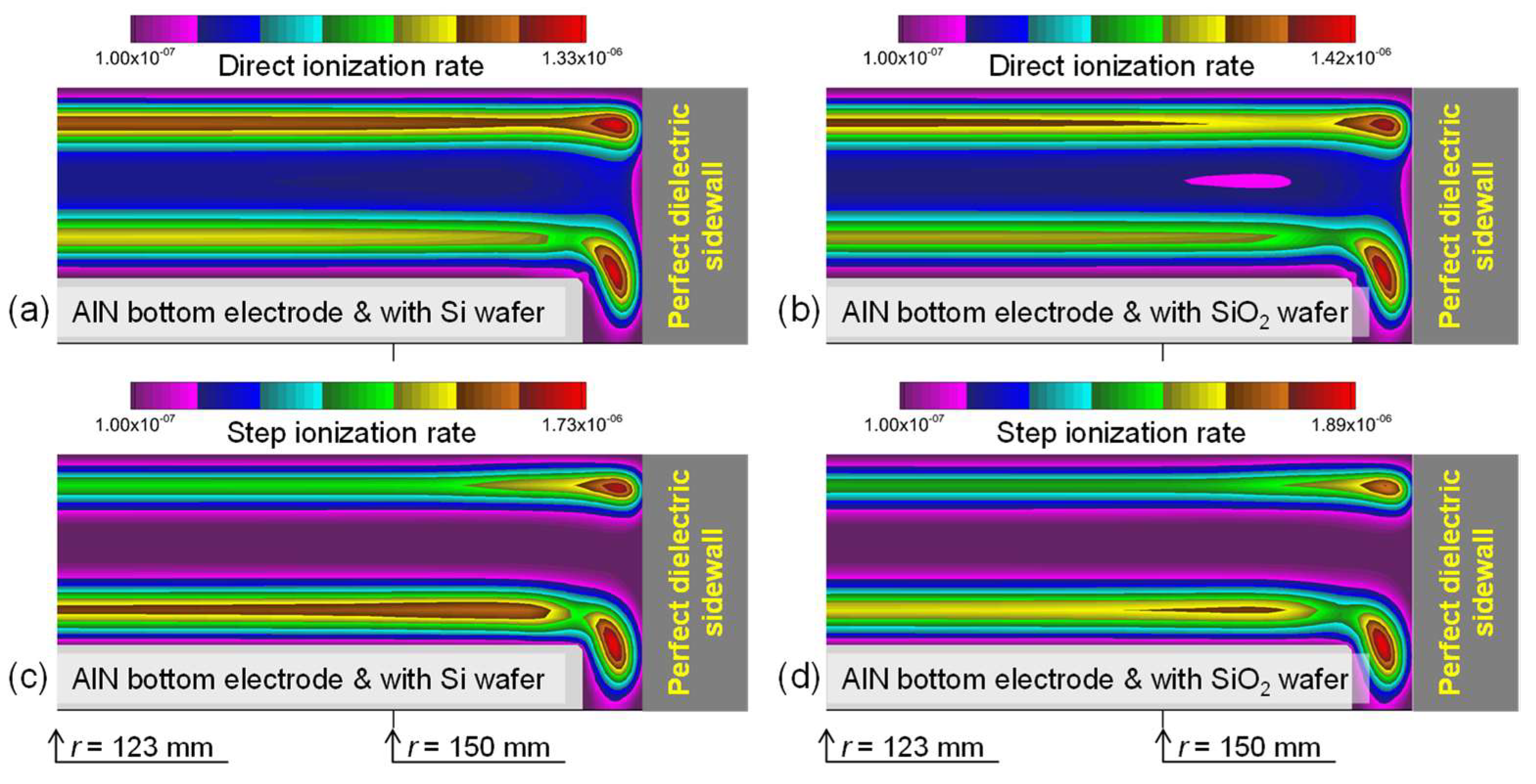
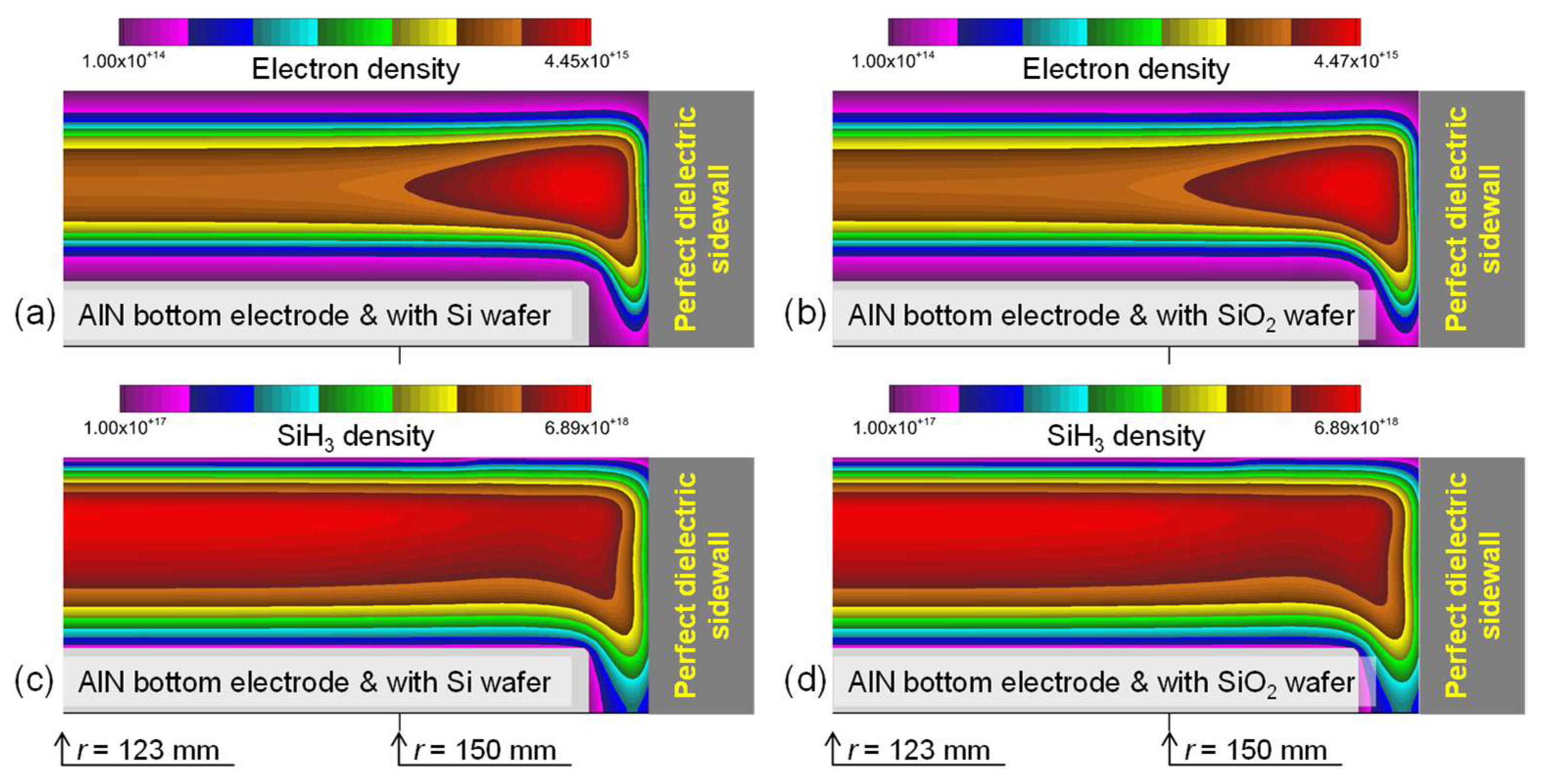
3.3. Effects of the Dielectric Wafer and the Perfect Dielectric Sidewall

The effects of the electrical conditions of the sidewall surface were investigated by replacing the quartz sidewall with a perfect dielectric in Cases 6 and 7 (See Table 1). The other conditions of Cases 6 and 7 were identical to those of Cases 4 and 5. The time-averaged results for Case 6 (case with the perfect dielectric sidewall, the AlN bottom electrode, and the Si wafer) and Case 7 (case with the perfect dielectric sidewall, the AlN bottom electrode, and the SiO2 wafer) are depicted and compared in Figure 5 and Figure 6.
The adoption of the perfect dielectric sidewall means that with the insulating sidewall having a higher impedance than the previous cases, the electrodes have a more comparable effective size. Thus, regardless of the dielectric constant of the wafer, the degree of asymmetricity of the ionization rate is efficiently reduced. The ionization rate is noticeably lower near the boundary between the bulk and the bottom sheath without a significant change in the bulk plasma region. These effects flatten the peak of the ion density profile by reducing the accumulation of charged species in this region. This ensures that the ion density and flux profiles in the radial direction become more uniform. As shown for these cases in Figure 5, peak values of ionization rates are detected near the corners of the reactor, near the intersection of the axial and radial sheaths. In contrast, ionization rates (i.e., the rate at which SiH2+ is produced) show relatively lower values and are evenly distributed within the interelectrode region. The ionization rates are more vertically symmetric in Cases 6 and 7 than they are in Cases 4 and 5. This is because they are more localized near the top and bottom sidewalls.
In Figure 6a,b, the electron density distributions at the interelectrode regions are fairly flat in both Cases 6 and 7. In addition, the peak values (Neo) of Cases 6 and 7 are lower than those of the other previous cases (except for Case 3), and compared to previous cases, the electron density distributions penetrate the gap between the bottom electrode and the sidewall more deeply. The contours of Cases 6 and 7 (Figure 6c,d) depict the spatial variations in the time-averaged SiH3 densities (m−3). Note that for these two cases, the peak values of the SiH3 densities are detected only near the reactor axis (i.e., the on-axis maximum). For both Cases 6 and 7, the distribution characteristics of the SiH3 density change from corner-dominated to bulk-dominated as a result of the shift in the radial position of peak value. The changes are the result of non-negligible differences between plasma parameter peak values.

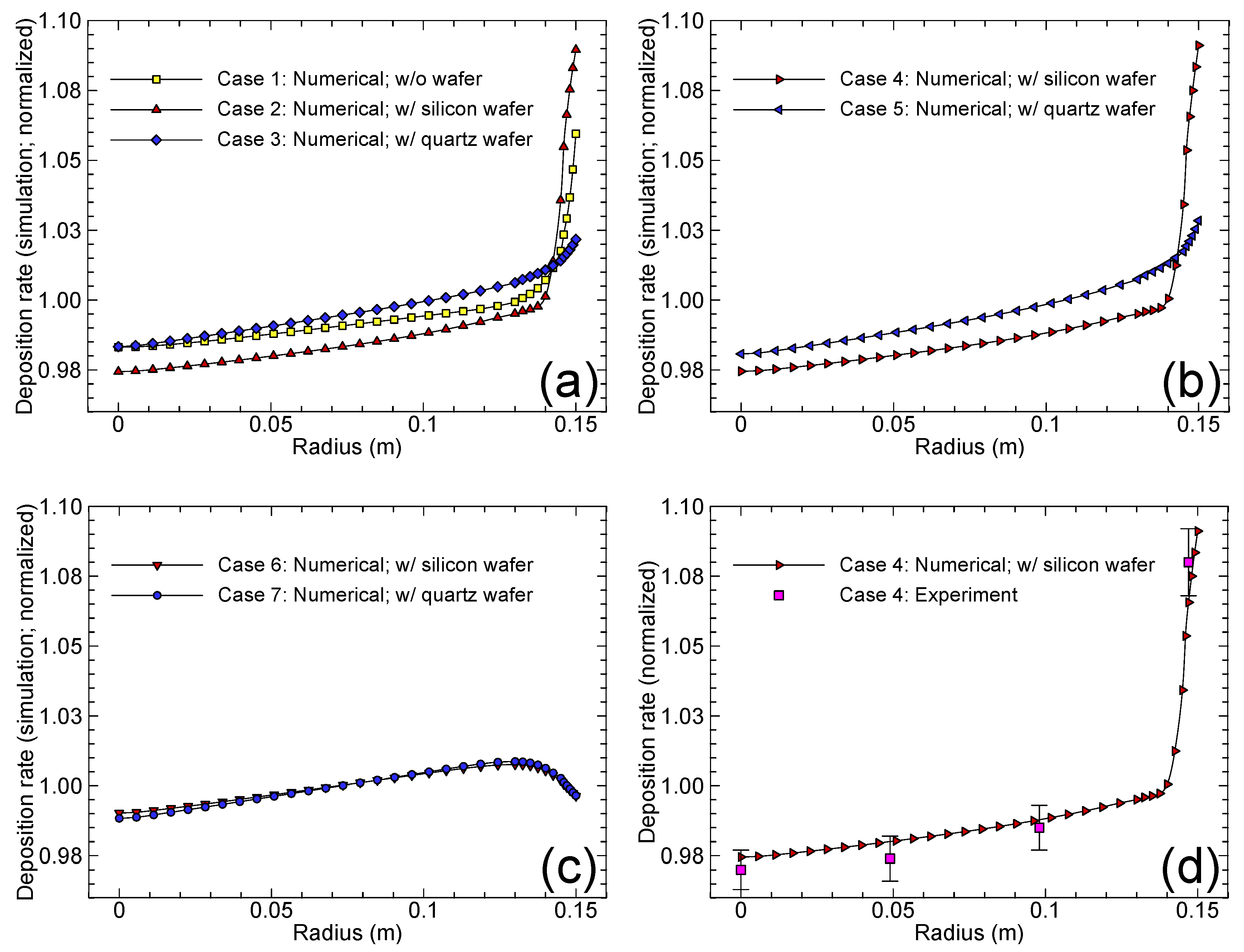
3.4. Deposition Rate Profiles

This section discusses the effects of dielectric elements on the deposition rate profiles. In Figure 7a, the deposition rate profiles are plotted for Case 1 (the aluminum bottom electrode without the wafer and the SiO2 sidewall), Case 2 (the aluminum bottom electrode with the Si wafer and the SiO2 sidewall), and Case 3 (the aluminum bottom electrode with the SiO2 wafer and the SiO2 sidewall). In Figure 7b, the deposition rate profiles are plotted for Case 4 (the AlN bottom electrode with the Si wafer and the SiO2 sidewall) and Case 5 (the AlN bottom electrode with the SiO2 wafer and the SiO2 sidewall). In Figure 7c, the deposition rate profiles are plotted for Case 6 (the AlN bottom electrode with the Si wafer and the perfect dielectric sidewall) and Case 7 (the AlN bottom electrode with the SiO2 wafer and the perfect dielectric sidewall). In addition, the experimental data of Case 4 are superimposed on the profile of Case 4 in Figure 7d. Profiles are normalized with their corresponding average values in order to facilitate comparison of spatial features.
As shown by the plots in Figure 7, the deposition rate profiles of Cases 1, 2, and 4 increase faster near the electrode edge and they have a similar appearance. These nonuniformities can be explained in terms of the enhanced flux and thus the thinner boundary layer of SiH3 density near the electrode edge. In order to understand the higher SiH3 surface flux, it may be helpful to consider how the electron impact dissociation is enhanced by the Neo at the surface and, therefore, excess SiH3 is produced and carried to the wafer surface. In Case 4, the fast increase in the deposition rate near the wafer edge is confirmed by comparing the simulation results with experimental data, as shown in Figure 7d.
However, the deposition rate profiles of Cases 3, 5, 6, and 7 indicate that their uniformities have noticeably improved by incorporating the dielectric elements such as the SiO2 wafer and the perfect dielectric sidewall. As stated above, the dielectric elements have the effect of decreasing the axial (vertical) asymmetries of the distributions of the plasma parameters. Additionally, peak ionization rates increase, and their radial position shifts away from the wafer edge, causing more uniform distributions of electrons and SiH3 close to the wafer edge. Cases 6 and 7 exhibit uniform deposition profiles (about 2.0%) as a result of the combination of these effects. Furthermore, previous related literature observed effects of dielectric elements [15,16,17,18,19].

4. Discussion

In combination, the results of this study indicate that modulation of the dielectric elements is useful for the modulation of the position and the peak values of the plasma parameters such as the off-axis maximum of the electron density (Neo). It is demonstrated that Neo’s observations conform to the expectation derived from the conclusion that the largest electric fields are found at the electrode edges. As a result of radial drift, the electron density accumulates at the electrode edge, which results in an off-axis maximum, as shown in Figure 2c for Case 1, Figure S2a for Case 2 (See the Supplementary Materials), Figure S2b for Case 3 (See the Supplementary Materials), Figure 4a for Case 4, Figure 4b for Case 5, Figure 6a for Case 6, and Figure 6b for Case 7. A feature of the CCP discharge structure has been reported in several studies to include Neo both numerically and experimentally.
With regard to electron heating rate, which is defined as −e Je · E in Equation (2), the increase in the strength of electric field will cause the electron temperature to rise, which will then result in an increase in the ionization rate coefficients, which will then produce an increase in the electron density. The resulting increase in electron density, combined with an increase in electron temperature, causes the ionization reaction rate near the corners of the reactor to increase. Thus, as depicted in Figure 2a for Case 1, Figure S1a for Case 2 (see the Supplementary Material), Figure S1b for Case 3 (see the Supplementary Material), Figure 3a for Case 4, Figure 3b for Case 5, Figure 5a for Case 6, and Figure 5b for Case 7, the higher ionization rates at the corners can be explained by the enhancement of the electric field, which increases the electron heating rate.
RF currents are partially excluded by the floating bottom (axial) sheath induced by the nonconducting wafer without causing an excessive amount of electron heating. Thus, Figure 3 shows that the ionization rate of Case 4 is higher than that of Case 5 near the wafer edge, and Figure 5 shows that the ionization rate of Case 6 is higher than that of Case 7 near the wafer edge.
Additionally, in Cases 6 and 7, the electron densities are spread out to a greater extent into the narrow bottom region between the bottom electrode edge and the bottom sidewall than they are in Cases 4 and 5. This would be attributed to the presence of a perfect dielectric sidewall, causing greater (axial) ion currents and (vertical) penetration of the electron density, both of which were observed to produce a reduction in the axial (vertical) asymmetries of the distribution of the plasma parameters.

5. Conclusions

In this study, a two-dimensional self-consistent fluid model was employed to numerically investigate the influence of the dielectric elements, namely, the nonconducting wafer, nonconducting sidewall, and ceramic electrode, on the radial uniformity of the plasma in a CCP reactor for the 300 mm wafer process. A series of numerical simulations was conducted for SiH4/He discharges at the pressure of 1200 Pa and frequency of 13.56 MHz. The results indicate that the plasma parameters strongly depend on the placement or installation of the dielectric elements.
It should be noted that in Case 1, since the aluminum bottom electrode was adopted without a wafer, the plasma parameters were localized and focused in a narrow vicinity of the bottom electrode edge. In Cases 2 and 3 as well as in Cases 4 and 5, the wafer material was changed from Si to SiO2. Despite the thinness of the wafer, as the dielectric constant of the wafer decreased, the electric field at the wafer edge weakened owing to the stronger surface-charging effect. Further, in Cases 4 and 5, the material of the bottom electrode was changed from Al to AlN in both cases. Lastly, in Cases 6 and 7, the perfect dielectric sidewall induced radially uniform plasma. These modifications were necessary because the radial positions of the peak values of the plasma parameters were moved away from the wafer edge. Based on these results, it could be concluded that plasma uniformity and thus deposition uniformity could be realized by selecting the optimal combination of dielectric elements.

Supplementary Materials

The following supporting information can be downloaded at: https://www.mdpi.com/article/10.3390/coatings12040457/s1: Figure S1: Effects of the dielectric constant of the wafer on the spatial distribution of the plasma parameters. Contour plots for the spatial profiles of the time-averaged SiH2+ production rate (kmol·m−3·s−1) for (a) Case 2 and (b) Case 3 for r ≥ 123 mm. Contour plots for the spatial profiles of the time-averaged Si+ production rate (kmol·m−3·s−1) (c) for Case 2 and (d) for Case 3 for r ≥ 123 mm. The profiles are radially uniform for r < 123 mm; Figure S2: Effects of the dielectric constant of the wafer on the spatial distribution of the plasma parameters. Contour plots for the spatial profiles of the time-averaged electron density (m−3) for (a) Case 2 and (b) Case 3 for r ≥ 123 mm. Contour plots for the spatial profiles of the time-averaged SiH3 density (m−3) (c) for Case 2 and (d) for Case 3 for r ≥ 123 mm. The profiles are radially uniform for r < 123 mm.

Funding

This work was supported by the Gachon University research fund of 2019 (GCU-2019-0814) and the National Research Council of Science & Technology (NST) grant by the Korea government (MSIT) (No. CRC-20-01-NFRI).

Institutional Review Board Statement

Not applicable.

Informed Consent Statement

Not applicable.

Data Availability Statement

The authors confirm that the data supporting the findings of this study are available within the article.

Conflicts of Interest

The authors declare no conflict of interest.

References

  1. Liang, Y.-S.; Liu, Y.-X.; Zhang, Y.-R.; Wang, Y.-N. Fluid simulation and experimental validation of plasma radial uniformity in 60MHz capacitively coupled nitrogen discharges. J. Appl. Phys. 2015, 117, 083301. [Google Scholar] [CrossRef]
  2. Liang, Y.-S.; Liu, G.-H.; Xue, C.; Liu, Y.-X.; Wang, Y.-N. Fluid simulation of species concentrations in capacitively coupled N2/Ar plasmas: Effect of gas proportion. J. Appl. Phys. 2017, 121, 203302. [Google Scholar] [CrossRef]
  3. Lieberman, M.A.; Lichtenberg, A.J. Principles of Plasma Discharges and Materials Processing; John Wiley & Sons, Inc.: New Jersey, NY, USA, 2005. [Google Scholar]
  4. Yavas, O.; Richter, E.; Kluthe, C.; Sickmoeller, M. Wafer-edge yield engineering in leading-edge DRAM manufacturing. Semicond. Fabtech 2009, 39, 1–5. [Google Scholar]
  5. Hwang, S.; Kanarik, K. Available online: https://sst.semiconductor-digest.com/2016/08/evolution-of-across-wafer-uniformity-control-in-plasma-etch/ (accessed on 27 February 2022).
  6. Kim, H.J. Effect of electrode heating on the distribution of the ion production rate in a capacitively coupled plasma deposition reactor in consideration of thermal decomposition. Vacuum 2021, 189, 110264. [Google Scholar] [CrossRef]
  7. Kim, H.J. Influence of the gas pressure in a Torr regime capacitively coupled plasma deposition reactor. Plasma Sources Sci. Technol. 2021, 30, 065001. [Google Scholar] [CrossRef]
  8. Bera, K.; Rauf, S.; Ramaswamy, K.; Collins, K. Effects of interelectrode gap on high frequency and very high frequency capacitively coupled plasmas. J. Vac. Sci. Technol. A 2009, 27, 706. [Google Scholar] [CrossRef]
  9. Bera, K.; Rauf, S.; Ramaswamy, K.; Collins, K. Control of plasma uniformity in a capacitive discharge using two very high frequency power sources. J. Appl. Phys. 2009, 106, 033301. [Google Scholar] [CrossRef]
  10. Kim, H.J.; Lee, H.J. 2D fluid model analysis for the effect of 3D gas flow on a capacitively coupled plasma deposition reactor. Plasma Sources Sci. Technol. 2016, 25, 035006. [Google Scholar] [CrossRef]
  11. Kim, H.J.; Lee, H.J. Numerical analysis of the effect of electrode spacing on deposition rate profiles in a capacitively coupled plasma reactor. Plasma Sources Sci. Technol. 2016, 25, 065006. [Google Scholar] [CrossRef]
  12. Kim, H.J.; Lee, H.J. Analysis of intermediate pressure SiH4/He capacitively coupled plasma for deposition of an amorphous hydrogenated silicon film in consideration of thermal diffusion effects. Plasma Sources Sci. Technol. 2017, 26, 085003. [Google Scholar] [CrossRef]
  13. Kim, H.J.; Lee, H.J. Uniformity control of the deposition rate profile of a-Si:H film by gas velocity and temperature distributions in a capacitively coupled plasma reactor. J. Appl. Phys. 2018, 123, 113302. [Google Scholar] [CrossRef]
  14. Xu, X.; Zhao, S.-X.; Zhang, Y.-R.; Wang, Y.-N. Phase-shift effect in capacitively coupled plasmas with two radio frequency or very high frequency sources. J. Appl. Phys. 2010, 108, 043308. [Google Scholar] [CrossRef]
  15. Kawamura, E.; Wen, D.-Q.; Lieberman, M.A.; Lichtenberg, A.J. Effect of a dielectric layer on plasma uniformity in high frequency electronegative capacitive discharges. J. Vac. Sci. Technol. A 2017, 35, 05C311. [Google Scholar] [CrossRef]
  16. Jia, W.-Z.; Liu, R.-Q.; Wang, X.-F.; Liu, X.-M.; Song, Y.-H.; Wang, Y.-N. Two-dimensional fluid simulation of a radio frequency capacitively coupled plasma in SiH4/N2/O2. Phys. Plasmas 2018, 25, 093501. [Google Scholar] [CrossRef]
  17. Liu, Y.; Booth, J.-P.; Chabert, P. Plasma non-uniformity in a symmetric radiofrequency capacitively-coupled reactor with dielectric side-wall: A two dimensional particle-in-cell/Monte Carlo collision simulation. Plasma Sources Sci. Technol. 2018, 27, 025006. [Google Scholar] [CrossRef]
  18. Wang, J.-C.; Tian, P.; Kenney, J.; Rauf, S.; Korolov, I.; Schulze, J. Ion energy distribution functions in a dual-frequency low-pressure capacitively-coupled plasma: Experiments and particle-in-cell simulation. Plasma Sources Sci. Technol. 2021, 30, 075031. [Google Scholar] [CrossRef]
  19. Ouyang, W.; Ding, C.; Liu, Q.; Gao, S.; Deng, W.; Wu, Z. Fluid simulation of the plasma uniformity in new multi-directional source capacitively coupled plasma. AIP Adv. 2021, 11, 075121. [Google Scholar] [CrossRef]
  20. Yang, Y.; Kushner, M.J. Fluid simulation of the plasma uniformity in new multi-directional source capacitively coupled plasma. J. Phys. D Appl. Phys. 2010, 43, 152001. [Google Scholar] [CrossRef] [Green Version]
  21. Dalvie, M.; Surendra, M.; Selwyn, G.S. Self-consistent fluid modeling of radio frequency discharges in two dimensions. Appl. Phys. Lett. 1993, 62, 3207. [Google Scholar] [CrossRef]
  22. Bi, Z.-H.; Dai, Z.-L.; Zhang, Y.-R.; Liu, D.-P.; Wang, Y.-N. Effects of reactor geometry and frequency coupling on dual-frequency capacitively coupled plasmas. Plasma Sour. Sci. Technol. 2013, 22, 055007. [Google Scholar] [CrossRef]
  23. Kim, H.C.; Manousiouthakis, V.I. Simulation based plasma reactor design for improved ion bombardment uniformity. J. Vac. Sci. Technol. B 2000, 18, 841. [Google Scholar] [CrossRef]
  24. Michna, T.; Ellingboe, A.R. Characterisation of an RF power splitter for multi-tile PECVD systems application. Curr. Appl. Phys. 2011, 11, S9–S11. [Google Scholar] [CrossRef]
  25. Kim, H.J. Enhancement of cleanliness and deposition rate by understanding the multiple roles of the showerhead electrode in a capacitively coupled plasma reactor. Coatings 2021, 11, 999. [Google Scholar] [CrossRef]
  26. Group, E. CFD-ACE+ 2020.0 Manual; ESI US R&D Inc.: Huntsville, AL, USA, 2020. [Google Scholar]
  27. Batey, J.; Tierney, E.; Stasiak, J.; Nguyen, T.N. Plasma-enhanced CVD of high quality insulating films. Appl. Surf. Sci. 1989, 39, 1–15. [Google Scholar] [CrossRef]
  28. Beckman, M.W. The Effects of Low Pressure Helium Ion Bombardment on Hydrogenated Amorphous Silicon. Master’s Thesis, Iowa State University, Ames, IA, USA, 2008. [Google Scholar]
  29. Bhattacharya, K.; Das, D. Effect of deposition temperature on the growth of nanocrystalline silicon network from helium diluted silane plasma. J. Phys. D: Appl. Phys. 2008, 41, 155420. [Google Scholar] [CrossRef]
  30. Kushner, M.J. Simulation of the gas-phase processes in remote-plasma-activated chemical-vapor deposition of silicon dielectrics using rare gas-silane-ammonia mixtures. J. Appl. Phys. 1992, 9, 4173–4189. [Google Scholar] [CrossRef] [Green Version]
Figure 1. Schematic diagram of the CCP reactor: (a) spatial variation in the gas temperature (Tg, K). Contour plots of the spatial profiles of (b) He* production rate and (c) He density (m−3) for r ≥ 123 mm.
Coatings 12 00457 g001
Figure 2. Contour plots for the spatial profiles of the time-averaged (a) SiH2+ production rate for Case 1 and (b) Si+ production rate for Case 1 for r ≥ 123 mm. Contour plots for the spatial profiles of the time-averaged (c) electron density for Case 1 and (d) SiH3 density for Case 1 for r ≥ 123 mm. The profiles are radially uniform for r < 123 mm.
Coatings 12 00457 g002
Figure 3. Effects of the dielectric constant of the wafer on the spatial distribution of the plasma parameters. Contour plots for the spatial profiles of the time-averaged SiH2+ production rate (kmol·m−3·s−1) for (a) Case 4 and (b) Case 5 for r ≥ 123 mm. Contour plots for the spatial profiles of the time-averaged Si+ production rate (kmol·m−3·s−1) (c) for Case 4 and (d) for Case 5 for r ≥ 123 mm. The profiles are radially uniform for r < 123 mm.
Coatings 12 00457 g003
Figure 4. Effects of the dielectric constant of the wafer on the spatial distribution of the plasma parameters. Contour plots for the spatial profiles of the time-averaged electron density (m−3) for (a) Case 4 and (b) Case 5 for r ≥ 123 mm. Contour plots for the spatial profiles of the time-averaged SiH3 density (m−3) (c) for Case 4 and (d) for Case 5 for r ≥ 123 mm. The profiles are radially uniform for r < 123 mm.
Coatings 12 00457 g004
Figure 5. Effects of the dielectric constant of the wafer on the spatial distribution of the plasma parameters. Contour plots for the spatial profiles of the time-averaged SiH2+ production rate (kmol·m−3·s−1) for (a) Case 6 and (b) Case 7 for r ≥ 123 mm. Contour plots for the spatial profiles of the time-averaged Si+ production rate (kmol·m−3·s−1) (c) for Case 6 and (d) for Case 7 for r ≥ 123 mm. The profiles are radially uniform for r < 123 mm.
Coatings 12 00457 g005
Figure 6. Effects of the dielectric constant of the wafer on the spatial distribution of the plasma parameters. Contour plots for the spatial profiles of the time-averaged electron density (m−3) for (a) Case 6 and (b) Case 7 for r ≥ 123 mm. Contour plots for the spatial profiles of the time-averaged SiH3 density (m−3) (c) for Case 6 and (d) for Case 7 for r ≥ 123 mm. The profiles are radially uniform for r < 123 mm.
Coatings 12 00457 g006
Figure 7. Effect of the dielectric components on the deposition rates. Deposition rate profiles for (a) Case 1, Case 2, and Case 3; (b) Case 4 and Case 5; (c) Case 6 and Case 7. (d) Experimental data of Case 4 superimposed on the profile of Case 4. The profiles are normalized with their corresponding averaged values.
Coatings 12 00457 g007
Table 1. List of cases considered in this study.
Case No.Wafer
Material
Electrode
Material
Sidewall
Material
1 (base)NoneAluminumSiO2; k = 3.9
2Si; k = 11.7AluminumSiO2; k = 3.9
3SiO2; k = 3.9AluminumSiO2; k = 3.9
4Si; k = 11.7Aluminum Nitride; k = 8.9SiO2; k = 3.9
5SiO2; k = 3.9Aluminum Nitride; k = 8.9SiO2; k = 3.9
6Si; k = 11.7Aluminum Nitride; k = 8.9Perfect Dielectric
7SiO2; k = 3.9Aluminum Nitride; k = 8.9Perfect Dielectric
Publisher’s Note: MDPI stays neutral with regard to jurisdictional claims in published maps and institutional affiliations.

