Article

Comparison of Various Thin-Film-Based Absorber Materials: A Viable Approach for Next-Generation Solar Cells

1
Academy of Scientific and Innovative Research (AcSIR), Ghaziabad 201002, India
2
Indian Reference Materials (BND) Division, CSIR-National Physical Laboratory, Dr. K. S. Krishnan Marg, New Delhi 110012, India
*
Authors to whom correspondence should be addressed.
Coatings 2022, 12(3), 405; https://doi.org/10.3390/coatings12030405
Submission received: 18 February 2022 / Revised: 12 March 2022 / Accepted: 16 March 2022 / Published: 18 March 2022
(This article belongs to the Section Thin Films)

Abstract

:
Thin-film solar cells are simple and affordable to produce, but their efficiency is low compared to crystalline-silicon solar cells, and needs to be improved. This study investigates the photovoltaic performance of different absorber materials (CdTe, CIGS, Sb2Se3, and CZTS) with simple structure Au/absorber/CdS/ITO. The research uses the SCAPS (Solar Cell Capacitance Simulator), a mathematical model based on Poisson and continuity equations. The impact of various parameters on cell performance, such as absorber layer thickness, acceptor density, electron affinity, back contact work function, and temperature, are examined. As per the simulation results, an absorber thickness of 4 µm is suitable for achieving the maximum efficiency for all the absorber materials. The optimized acceptor density for CdTe/CIGS/ Sb2Se3 and CZTS is taken as 1016 cm−3 and 1017 cm−3, respectively. The back contact work function and device temperature were set to be 5.1 eV and 300 K, respectively, to achieve excellent performance. Among all the absorber materials, the highest efficiency of 28.2% was achieved for CZTS. The aim is to highlight the various absorber layers’ performances by optimizing the device parameters. The obtained results can be used in solar energy harvesting applications due to the improved performance characteristics.
Keywords:
CdTe; CIGS; Sb2Se3; CZTS; SCAPS

1. Introduction

The buffer layer is another critical layer in heterojunction solar cell design. CdS is a semiconductor of the II-VI group with a 2.45 eV energy band gap [1]. Researchers have been drawn towards CdS thin film for a long time because of its fascinating optoelectronic features, and it is commonly utilized as a buffer layer in solar cells. Another exciting aspect of this material is that it gives the absorber layer chemical and thermal stability. The buffer layer forms a junction with the absorber layer, which improves the solar cell’s bulk recombination. The band gap energy (Eg) must be tuned to ~1.5 eV to perform well. Cadmium-telluride (CdTe), Copper-indium-gallium-diselenide (CIGS), Copper-zinc-tellurium selenide (CZTS), and Antimony selenide (Sb2Se3) thin film-based solar cells are known to be promising options for solar cell technology because of their excellent performance, high efficiency, and low cost [2,3,4,5]. CIGS-based solar cells have already crossed 20% efficiency [6]. Even though CIGS thin-film solar cells have come to the point of maturity where they can easily be mass-produced, specific improvements may be made to improve efficiency and lower the costs. CIGS is a chalcopyrite semiconductor having a high absorption coefficient and band gap of 1.06–1.7 eV [7], and the exact value of the band gap is determined by the “x” factor, which is the Ga/(Ga + In) ratio. Apart from the band gap and absorption coefficient, the thickness of the absorber layer is an integral part of the performance of photovoltaic devices. Tariq Alzoubi et al. has been achieved an efficiency of 21.35% and 24.21% with absorber thicknesses of 1500 nm and 2500 nm, respectively [8].
CdTe has become one of the best materials for fabricating solar cell devices, as it has a high absorption spectrum and optimal band gap of 1.5 eV. CdTe was developed as a semiconducting material that is appropriate for operating at high processing temperatures from the standpoint of production. The research on CdTe/CdS thin film-based solar cells started in the 1970s. The emergence of several methods such as electrodeposition, screen printing, vacuum evaporation, and close-spaced sublimation gave considerable impetus to research and developmenent (R&D) in the 1980s. Hence, CdTe/CdS solar cells with an efficiency above 10% were obtained [9,10]. The efficiency of solar cells based on CdTe/CdS thin films increased after 2011 and reached above 20%. Solar cell companies have led the solar cell market over the past decade, and they continue to produce highly efficient CdTe/CdS-based solar cells. The cost of CdTe-based solar cells is 30% lower than that of CIGS-based solar cells [11]. Many researchers have recently focused their attention on CZTS-based thin-film solar cells for several reasons [12,13], such as their high absorption coefficient, optimal band gap (1.4–1.5 eV), low cost, and high efficiency. Furthermore, for the research on thin-film solar cells, before experimental investigations, simulation is helpful to evaluate the effects of changes in solar cell characteristics. Khan et al. and Yasin et al. achieved an efficiency of 19.64% [14] and 28.41% [15], respectively, for CdS/CZTS-based solar structure by optimizing the various parameters of the device. The development of Sb2Se3-based solar cells has been rapid, with reported efficiencies of 9.2% for devices in substrate configuration, prompting more intensive research [16], as this material has a single-phase structure and highly anisotropic properties. Mu et al. applied CZTS as an Hole transport layer (HTL) layer to construct a Sb2Se3-based solar cell and achieved a 17.14% efficient solar cell [17]. Hedayati et al. achieved an efficiency of 11.38% for CGS/CIGS dual-junction solar cells by using a metal grid instead of Transparent conducting oxide (TCO) [18]. Minabashi et al. investigated earth-abundant and less toxic CZTSSe absorber materials in kesterite photovoltaic cells using the finite element method (FEM) and recorded 19.06% efficiency [19]. Najm et al. performed the numerical simulation to check the impact of electrical properties of CdS buffer layer for SLG/Mo/p-Absorber/n-CdS/n-ZnO/Ag (Soda lime glass (SLG)) solar cell structure [20].
The theoretical efficiency for Sb2Se3 has reached over 30%, comparable to CdTe and CIGS-based photovoltaic cells. Despite this improvement, further progress on the open-circuit voltage, current density, and fill factor is required to enhance Sb2Se3 solar cell efficiency. To date, research into these efficiency loss mechanisms is in its early stages, with little effort put in, preventing Sb2Se3 from becoming a high-efficiency and low-cost solar cell technique at the terawatt level. To improve Sb2Se3 solar cells’ efficiency, it is essential to identify the critical components behind the cause of efficiency loss. Here, SCAPS simulation software [21,22,23,24] is used to thoroughly analyze physical and electrical properties of various absorber layers-based solar cells, which provides new insights into the potential explanation of efficiency loss.

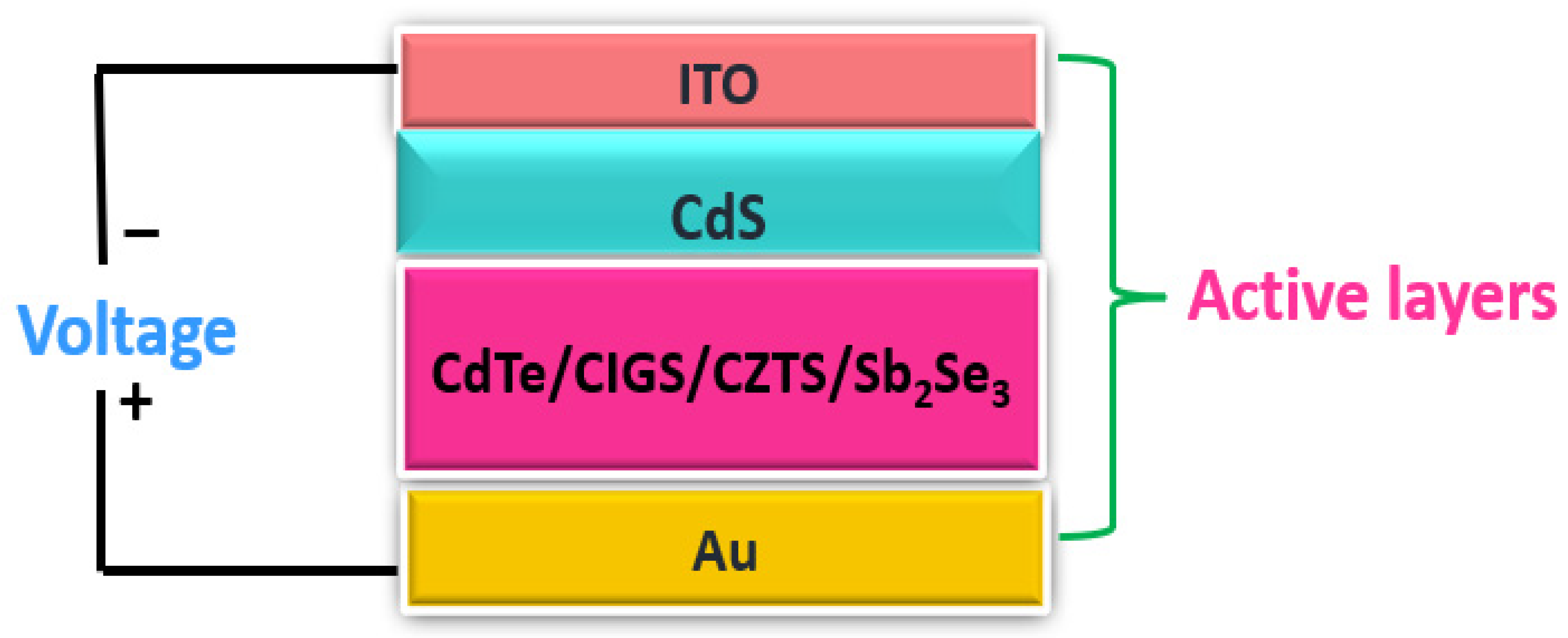
2. Device Modeling and Simulation Parameters

SCAPS is a numerical simulation software package that gives results close to reality. A set of coupled differential equations is produced by applying the appropriate boundary conditions at the contacts and interfaces. This software’s meshing algorithm employs coarse meshing in the center of the layer and fine meshing near the interface and contacts. During the calculations, the mesh is optimized, and by considering the effects of gradings, defects, and impurities on photovoltaic properties, optimizing mesh at each iteration step is easy. The simulation research defines the physical models of the absorber layer-based photovoltaic devices, highlighting new facts, and providing insight and a better platform for the further optimization of solar devices. This software uses the Poisson and continuity equations for holes and electrons as stated by Equations (1)–(3). By solving these equations, the I-V and C-V characteristics, energy band structures, etc., can be produced and used to compute various parameters.
d 2 dx 2   Ψ   ( x ) = e ε 0 ε r p ( x ) n ( x ) + N D N A + ρ P ρ n
dJ n dx = ( G R )
dJ p dx = ( G R )
Here, εr and ε0 are the relative and the vacuum permittivity, and Ψ is electrostatic potential. n and p represent the electron and hole concentration, ND and NA are the donor and acceptor impurity, respectively. R and G are recombination and generation rates, respectively.
Various output parameters such as open-circuit voltage (Voc), current density (Jsc), fill factor (FF), and efficiency (η) are optimized. Voc is the maximum voltage developed in a solar cell at zero current, which is affected by the temperature. FF depicts the maximum power produced by a photovoltaic cell after defining the squareness of the current density–voltage curve as presented by Equations (4) and (5), respectively. Efficiency is the ratio of output power to the input power, and it can also be defined by Equation (6):
V OC = nkT q ln   ( I L I O + 1 )   at   I = 0
FF = J max V max J sc V oc
η = J max V max P S
IL is the light-generated current, I0 is the dark saturation current, Jmax and Vmax are the maximum short-circuit current and open-circuit voltage, respectively, and PS is the sunlight’s incident power.
A simplified algorithm is used for the metal work function ϕ m (for majority carriers), which is taken as the input in SCAPS-1D software. If a p-type layer is adjacent to the contact, ϕ m is defined by Equation (7):
ϕ m = χ +   k B Tln ( N c / n i )
Here, χ is the electron affinity, NC and ni are the density of states and intrinsic carrier concentration, respectively.
The proposed device structure used in this study is Au/(CdTe or CIGS or CZTS or Sb2Se3)/CdS/ITO, as shown in Figure 1. Au is used as a back contact [25], ITO is front contact, CdTe, CIGS, CZTS, and Sb2Se3 are the absorber layers, and CdS is used as a buffer layer. In this work, SCAPS-1D simulation software (v3.3.10) is used for the numerical analysis of CdTe, CIGS, CZTS, and Sb2Se3-based solar cells. This software works based on the Poisson and Continuity equations [26,27]. The output parameters, such as I-V and C-V curves, energy bands, QE, etc., can be obtained by solving these equations. The material parameters of the various layers are chosen from theoretical and experimental data provided in earlier studies [28,29,30,31] as presented in Table 1. Absorber layer thicknesses and their shallow acceptor densities are varied to check the device’s performance. Modeled solar cell is exposed to AM 1.5 G solar light spectrum at its front contact with 1 (kW/m2) power. Au is used as back contact metal with a work function of 5.1 eV. To analyze the device’s performance, the work function value is varied from 4.4 to 5.1 eV.

3. Results and Discussions

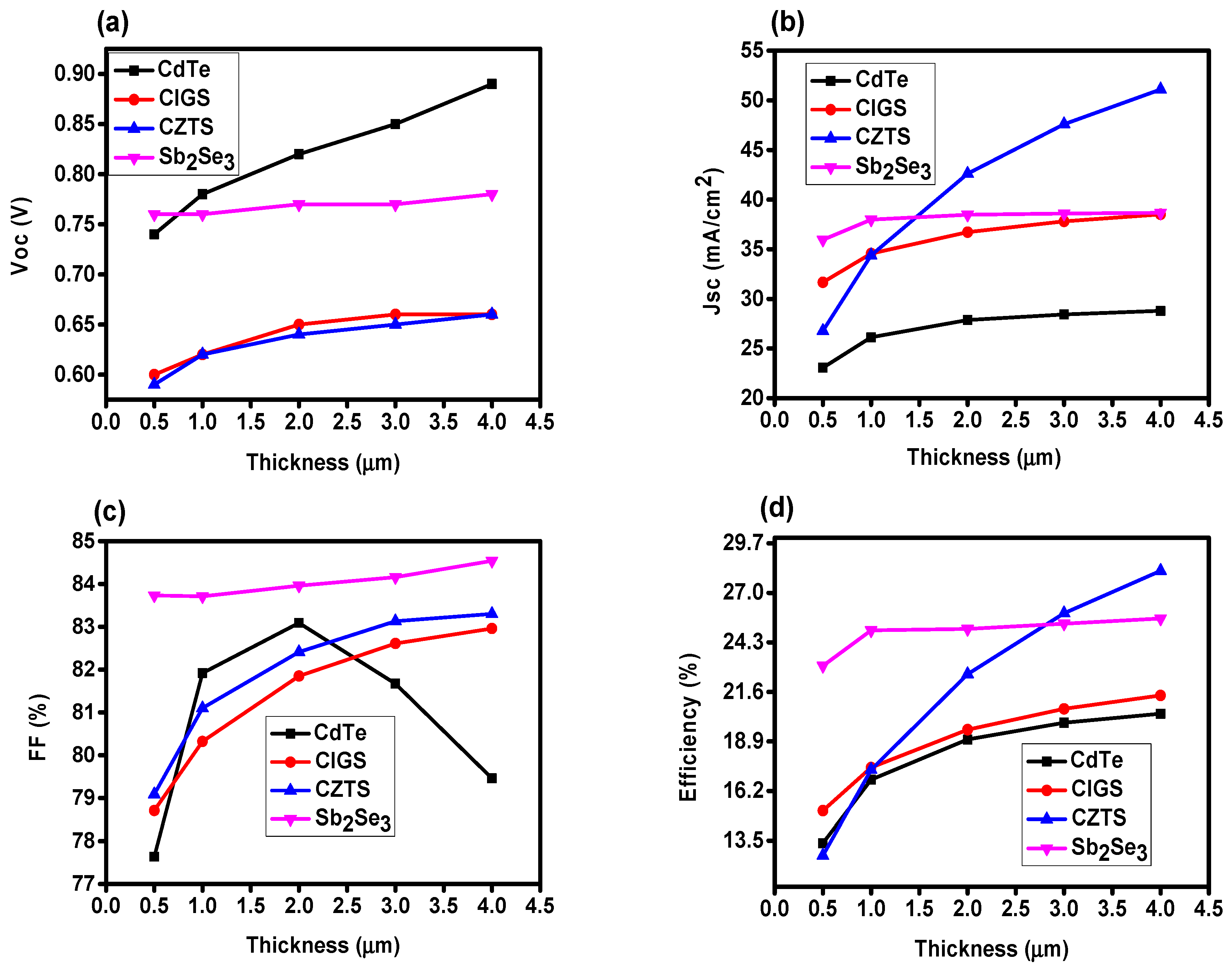
3.1. Influence of Absorber Layer Thickness on Device Performance

An absorber layer should be tuned to obtain the optimal thickness to absorb the maximum photons and produce electron–hole pairs. The thickness for all the absorber layers (CdTe, CIGS, CZTS, and Sb2Se3) was varied from 0.5 to 4 µm, and all other parameters were as reported in Table 1 and remained unchanged. Parameters such as open-circuit voltage (Voc), current density (Jsc), fill factor (FF), and efficiency (η) were affected by varying the absorber layer thickness, as presented in Figure 2a–d. These results show that Jsc, Voc, and η increase with increasing thickness for all absorber layers, as presented in Table 2. For CdTe, FF increases with thickness at first, then decreases as thickness increases from 2 to 4 µm, which can be attributed to increased series resistance. For other absorber layers, FF increases with the thickness. Thus, when the thickness of the absorber layer is too thin, it does not promote complete absorption of light, resulting in poor efficiency. If the absorber layer is too thick, the photo-generated carriers will have a lengthier transfer route, resulting in increased recombination. At a thickness of 4 µm, maximum efficiencies of 20.41%, 21.41%, 28.2%, and 25.6% were achieved for CdTe, CIGS, CZTS, and Sb2Se3, respectively.

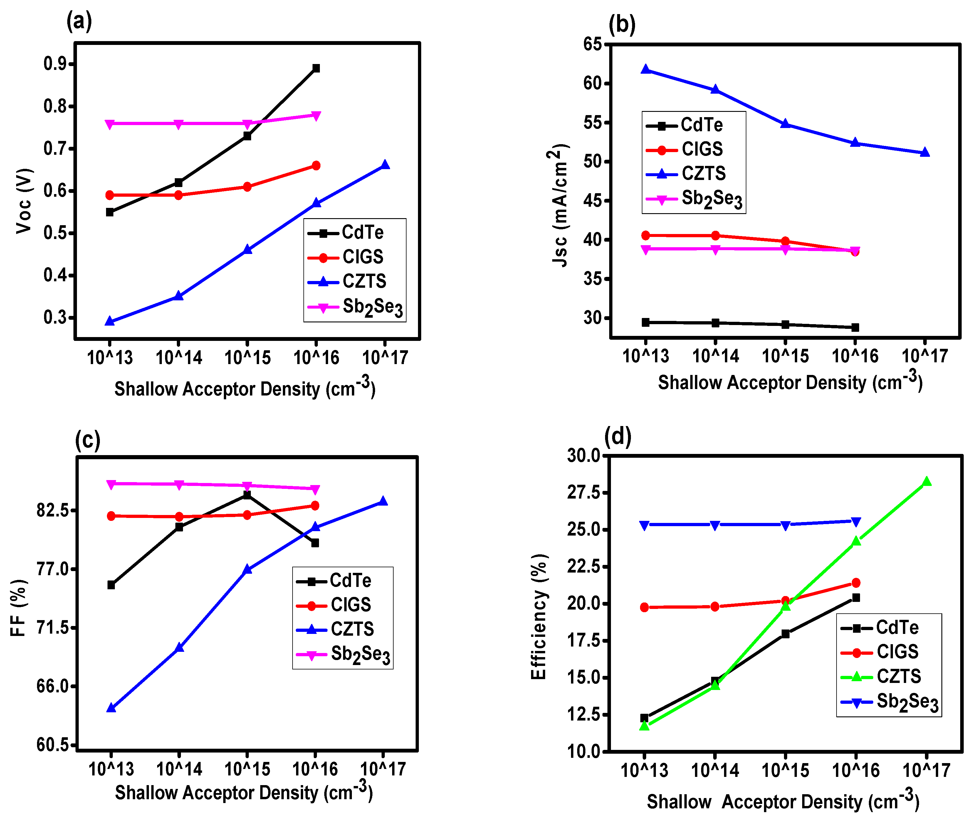
3.2. Effect of Absorber Layer Acceptor Density on Device Performance

Lower values of acceptor density can increase the series resistance, and larger values of acceptor density can reduce the shunt resistance, both of which can reduce the solar cell’s performance [32]. Figure 3 depicts the effect of acceptor density on Voc, Jsc, FF, and efficiency for the different absorber layers. For CdTe, CIGS, and Sb2Se3, Voc increases with acceptor density, peaking at 1016 cm−3 when the acceptor concentration is at its maximum. For CZTS, Voc reaches its maximum value at an acceptor density of 1017 cm−3. The built-in electric field of a photovoltaic cell can be enhanced by increasing the absorber’s acceptor concentration, which is advantageous for Voc [33]. The FF is less effective for CIGS and Sb2Se3 absorbers. For CZTS, FF increased up to 83.3%, and for CdTe, FF first increasedupto the acceptor density of 1015 cm−3 and then decreased. The efficiency of the cell is affected by changes in Voc, Jsc, and FF. The results show that maximum efficiency was achieved when the acceptor density was set to be 1016 and 1017 cm−3 for CIGS/CdTe/Sb2Se3 and CZTS, respectively. According to the analysis, the proper doping of the absorber layer can produce higher efficiency.

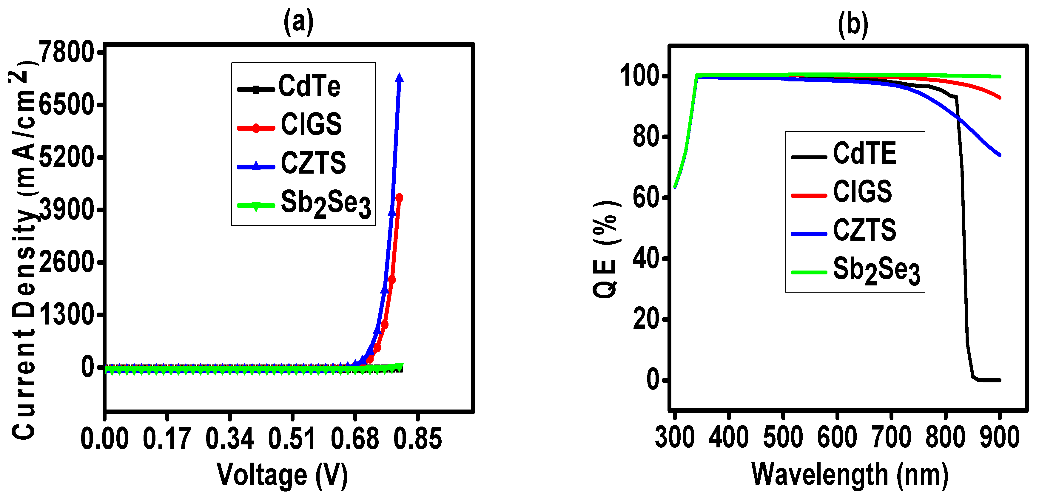
3.3. I-V and QE Characteristics for the Optimized Structures

Figure 4 shows the simulated I-V and QE characteristics of the optimized structure (Au/(CdTe or CIGS or CZTS or Sb2Se3)/CdS). The QE as a function of λ is defined as the ratio of current going through the circuit, i.e., the number of charge carriers produced and exiting the photovoltaic cell at the circuit, to the number of incoming photons. The optimized thickness for all the absorber layers was taken as 4 µm, and the optimized acceptor density for CdTe/CIGS/ Sb2Se3 and CZTS was taken as 1016 and 1017 cm−3, respectively. CZTS achieved the maximum efficiency compared to CdTe, CIGS, and Sb2Se3.

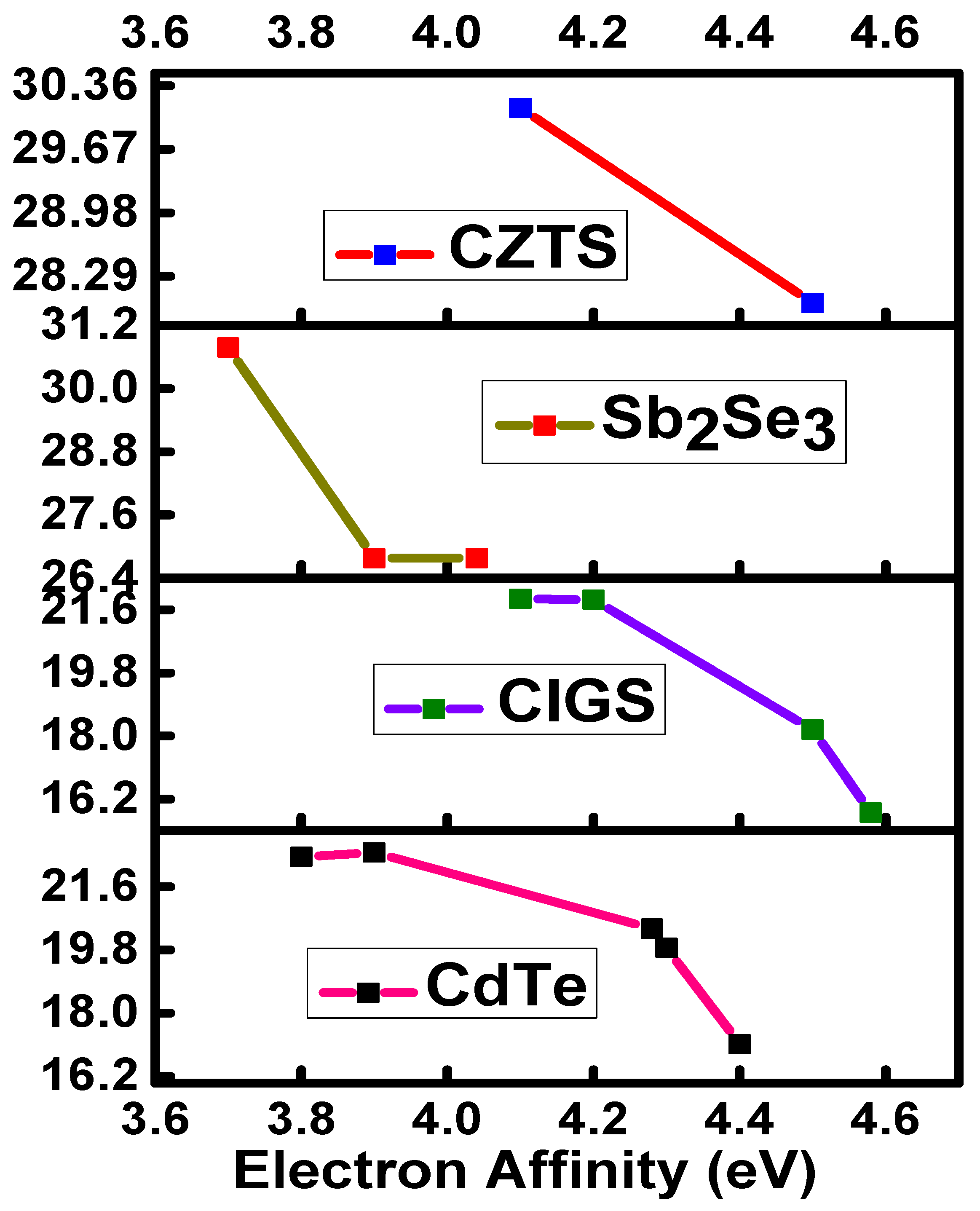
3.4. Effect of the Electron Affinity of Different Absorber Layers

At the connecting interface of the two semiconductors (here, the absorber and the buffer layer), electron affinity defines the conduction band offset. This offset significantly impacts the open-circuit voltage and short circuit current and the solar cell’s overall performance. In several simulation papers based on CdTe, CIGS, Sb2Se3 and CZTS solar cells, several values of electron affinity are used, as shown in Figure 5, such as for CdTe, 4.3 [34] and 4.4 [35], 3.9 [36] and 3.8 [37]; for CIGS, 4.45 [30], 4.2 [38] and 4.5 [39] and 4.58 [40]; for Sb2Se3, 3.9 [31], 3.7 [27], and for CZTS, 4.5 [28] and 4.1 [41]. As the electron affinity value increases, the efficiency decreases for all four absorber layers, because the enhanced electron affinity of the absorber layer decreases the number of photons hitting the absorber layer, the amount of current produced, and the short circuit current. An increase in barrier height makes it difficult to collect photo-generated charge carriers and reduces the device’s overall performance [42].

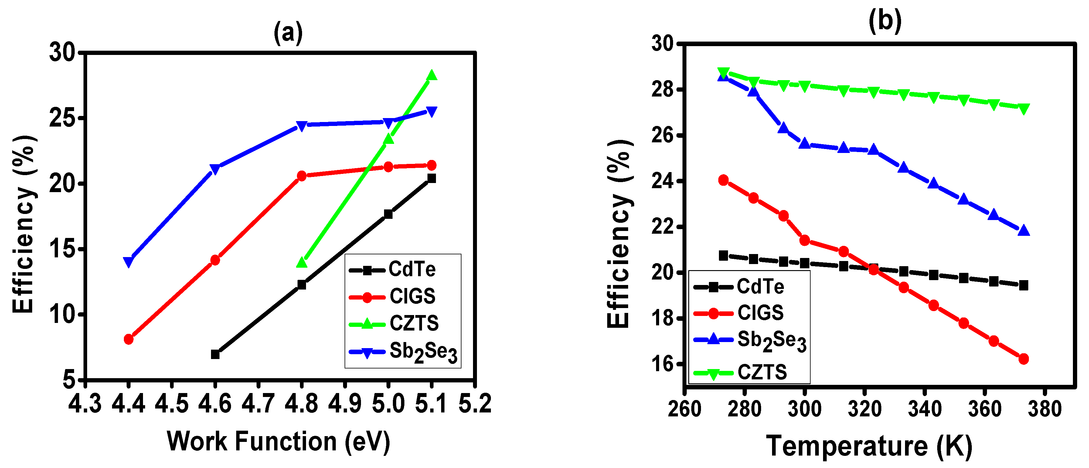
3.5. Effect of Back Contact Work Function and Temperature on Device Performance

To improve the performance of the solar cells, the back contact interface must be optimized. The back contact provides the ohmic contact for connections, and it should be corrosion-resistant and should have a low recombination rate for minority charge carriers [43]. We examined the effect of the work function on several parameters (Voc, Jsc, FF, and η) under optimum conditions, as shown in Figure 6a. The work function values was varied from 4.4 to 5.1 eV, and the analysis shows that the work function should be greater than 4.8 eV in order to achieve better efficiency. Below this work function value, the device performance can get degraded, as there is a significant energy-level discrepancy at the absorber layer/metal contact, resulting in the formation of a Schottky junction, decreasing device efficiency. Back energy band alignment is improved by increasing the work function value of the back contact metal. For all three absorber layer cases, maximum efficiency is achieved at 5.1 eV.
As the solar cells are set in open locations exposed to the sun, temperature increases are an issue in some areas where day temperatures are at their highest during the summer, thereby impacting the performance [44]. Efficiency slowly degrades with increasing temperature, as shown in Figure 6b, because when the temperature rises, the band gap of the Photovoltaic (PV) cell decreases, lowering the open-circuit voltage. Other parameters such as the band gap, carrier concentrations, and electron and hole mobility are all affected by the increased temperature. As a result, the efficiency of solar cells decreases. The highest efficiency was achieved at 280 K, but the Voc was beyond expected limit; thus, the overall performance looks to be more suitable at 300 K. Most semiconductor-based simulations are performed at this temperature, as it is closer to room temperature.

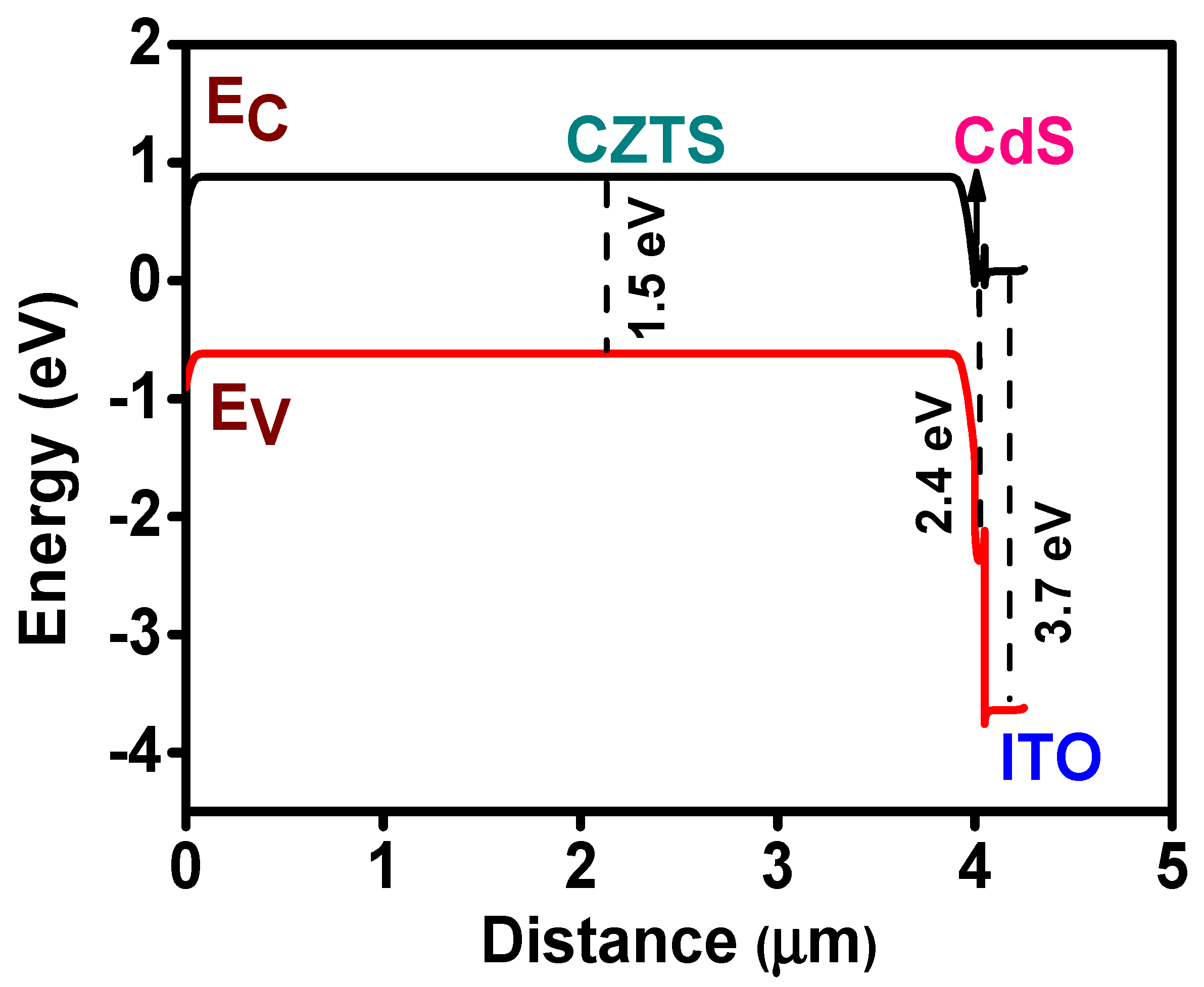
3.6. Energy Band Diagram of CZTS/CdS-Based Solar Cell

In an ideal semiconductor, electrons occupy the space below the valence band edge Ev and above the conduction band edge Ec. Between these two states, the electron population has no other energy level, and the energy difference between Ec and Ev is referred to as the band gap energy Eg, as stated in Equation (8). As a result, photon energy that is below this band gap energy value will not be absorbed.
Eg = Ec − Ev
Jia et al. and Rondiya et al. reported band gap values for CZTS of 1.5 and 1.49 eV, respectively, using density functional theory (DFT) [45,46]. Vadapoo et al. and Hasan et al. reported direct band gap values of 1.22 and 1.12 eV, respectively, for Sb2Se3 with the help of DFT [47,48]. Sarkar et al. calculated a band gap of 1.89 eV for CdTe by using the SCC-DFTB method [49].
The energy band diagram for the proposed solar structure of CZTS with conduction and valence band energies, Ec and Ev, respectively, is illustrated in Figure 7 based on the energy band panel data obtained from the SCAPS simulation showing the band gap of each material. The band gap values for CZTS, CdS, and ITO are 1.5, 2.4, and 3.7 eV, respectively. If the solar cell is exposed to photons with energies greater than the band gap energy, electron-hole pairs will form in the CZTS absorber. The photo-generated electrons will diffuse into the depleted space-charge area. The width of the space-charge area varies depending on the acceptor and donor density values of the absorber and buffer layers.
Thus, various parameters affect the overall performance of the solar cell. I-V characteristic measurements are insufficient to explain the behavior of a device in depth since the solar cell’s response is also dependent on its internal physical mechanism.

4. Conclusions

In this work, we studied the influence of various values of absorber layer thickness, acceptor density, electron affinity, back contact work function, and temperature on the performance of Au/(CdTe or CIGS or Sb2Se3 or CZTS)/CdS/ITO structures. In order to achieve excellent performance in the solar cell, the optimized thickness for all absorber layers was taken as 4 µm, and the optimized acceptor density for CdTe/CIGS/ Sb2Se3 and CZTS was taken as 1016 and 1017 cm−3, respectively. The efficiency increased with work function value because a higher back contact metal work function value enhances the back end energy band alignment. Temperature also affected the performance of the device, and the overall performance seemed to be more appropriate at 300 K for all absorber materials. Most semiconductor simulations are performed at this temperature, as this temperature is close to room temperature. After optimization of the device, CZTS showed excellent performance, with efficiency of 28.2%, compared to CdTe (20.41%), CIGS (21.41%) and Sb2Se3 (25.6%). Our findings may serve as a model for designing and fabricating cost-effective, efficient, and stable solar cells.

Author Contributions

M.: Data curation, Writing—original draft. K.K.M.: Writing—review & editing, Supervision. V.N.S.: Supervision, Writing—review & editing. All authors have read and agreed to the published version of the manuscript.

Funding

This research received no external funding.

Institutional Review Board Statement

Not applicable.

Informed Consent Statement

Not applicable.

Data Availability Statement

Data will be made available upon valid request.

Acknowledgments

Mamta highly acknowledges the Council for Scientific and Industrial Research (CSIR), India, for the Senior Research Fellowship (SRF) grant. The authors would like to thank their institute for its support. We also thank Professor Burgelman of the Gent University, Belgium, for providing the SCAPS program and using it.

Conflicts of Interest

The authors declare that they have no known competing financial interests or personal relationships that could have influenced the work reported in this paper.

References

  1. Oliva, A. Formation of the band gap energy on CdS thin films growth by two different techniques. Thin Solid Film. 2001, 391, 28–35. [Google Scholar] [CrossRef]
  2. Fang, Z.; Wang, X.C.; Wu, H.C.; Zhao, C.Z. Achievements and Challenges of CdS/CdTe Solar Cells. Int. J. Photoenergy 2011, 2011, 297350. [Google Scholar] [CrossRef]
  3. Powalla, M.; Paetel, S.; Hariskos, D.; Wuerz, R.; Kessler, F.; Lechner, P.; Wischmann, W.; Friedlmeier, T.M. Advances in Cost-Efficient Thin-Film Photovoltaics Based on Cu(In,Ga)Se2. Engineering 2017, 3, 445–451. [Google Scholar] [CrossRef]
  4. Guo, L.; Vijayaraghavan, S.; Duan, X.; Menon, H.G.; Wall, J.; Kong, L.; Gupta, S.; Li, L.; Yan, F. Stable and efficient Sb2Se3 solar cells with solution-processed NiOx hole-transport layer. Sol. Energy 2021, 218, 525–531. [Google Scholar] [CrossRef]
  5. Ojeda-Durán, E.; Monfil-Leyva, K.; Andrade-Arvizu, J.A.; Becerril-Romero, I.; Sánchez, Y.; Fonoll, R.; Guc, M.; Jehl, Z.; Luna-López, J.; Muñoz-Zurita, A.; et al. CZTS solar cells and the possibility of increasing VOC using evaporated Al2O3 at the CZTS/CdS interface. Sol. Energy 2020, 198, 696–703. [Google Scholar] [CrossRef]
  6. Jackson, P.; Hariskos, D.; Lotter, E.; Paetel, S.; Wuerz, R.; Menner, R.; Wischmann, W.; Powalla, M. New world record efficiency for Cu(In,Ga)Se2 thin-film solar cells beyond 20%. Prog. Photovolt. Res. Appl. 2011, 19, 894–897. [Google Scholar] [CrossRef]
  7. Oyedele, S.O.; Aka, B. Numerical Simulation of Varied Buffer Layer of Solar Cells Based on Cigs. Model. Numer. Simul. Mater. Sci. 2017, 7, 33–45. [Google Scholar] [CrossRef] [Green Version]
  8. Alzoubi, T.; Moustafa, M. Numerical optimization of absorber and CdS buffer layers in CIGS solar cells using SCAPS. Int. J. Smart Grid Clean Energy 2019, 8, 291–298. [Google Scholar] [CrossRef]
  9. Basol, B. Electrodeposited CdTe and HgCdTe solar cells. Sol. Cells 1988, 23, 69–88. [Google Scholar] [CrossRef]
  10. Mitchell, K.; Eberspacher, C.; Cohen, F.; Avery, J.; Duran, G.; Bottenberg, W. Progress towards high efficiency thin film CdTe solar cells. Sol. Cells 1988, 23, 49–57. [Google Scholar] [CrossRef]
  11. Sharma, S.; Jain, K.K.; Sharma, A. Solar Cells: In Research and Applications—A Review. Mater. Sci. Appl. 2015, 6, 1145–1155. [Google Scholar] [CrossRef] [Green Version]
  12. Rahaman, M.; Chowdhury, A.; Islam, M.; Rahman, M. CZTS BASED THIN FILM SOLAR CELL: An Investigation into the Influence of Dark Current on Cell Performance. In Proceedings of the 2018 Joint 7th International Conference on Informatics, Electronics & Vision (ICIEV) and 2018 2nd International Conference on Imaging, Vision & Pattern Recognition (icIVPR), Kitakyushu, Japan, 25–29 June 2018; pp. 87–92. [Google Scholar] [CrossRef]
  13. Suryawanshi, M.P.; Agawane, G.; Bhosale, S.M.; Shin, S.W.; Patil, P.S.; Kim, J.H.; Moholkar, A.V. CZTS based thin film solar cells: A status review. Mater. Technol. 2013, 28, 98–109. [Google Scholar] [CrossRef]
  14. Khan, R.; Ahmed, S.F.; Khalid, M.; Joshi, B. Investigating Effect of CdS Buffer Layer on the Performance of Cu2ZnSnS4 Based Solar Cells Using SCAPS-1D. Trans. Electr. Electron. Mater. 2020, 22, 177–184. [Google Scholar] [CrossRef]
  15. Yasin, S.; Abu Waar, Z.; Al Zoubi, T. Development of high efficiency CZTS solar cell through buffer layer parameters optimization using SCAPS-1D. Mater. Today Proc. 2020, 33, 1825–1829. [Google Scholar] [CrossRef]
  16. Li, Z.; Liang, X.; Li, G.; Liu, H.; Zhang, H.; Guo, J.; Chen, J.; Shen, K.; San, X.; Yu, W.; et al. 9.2%-efficient core-shell structured antimony selenide nanorod array solar cells. Nat. Commun. 2019, 10, 125. [Google Scholar] [CrossRef] [PubMed] [Green Version]
  17. Mu, F.; Liu, Z.; Zi, W.; Cao, Y.; Lu, X.; Li, Y.; Zhao, Z.; Xiao, Z.; Cheng, N. CZTS nanoparticles as an effective hole-transport layer for Sb2Se3 thin-film solar cells. Sol. Energy 2021, 226, 154–160. [Google Scholar] [CrossRef]
  18. Hedayati, M.; Olyaee, S. Proposal of CIGS dual-junction solar cell and investigation of different metal grids effect. Opt. Quantum Electron. 2020, 52, 347. [Google Scholar] [CrossRef]
  19. Minbashi, M.; Ghobadi, A.; Yazdani, E.; Kordbacheh, A.A.; Hajjiah, A. Efficiency enhancement of CZTSSe solar cells via screening the absorber layer by examining of different possible defects. Sci. Rep. 2020, 10, 21813. [Google Scholar] [CrossRef]
  20. Najm, A.S.; Chelvanathan, P.; Tiong, S.K.; Ferdaous, M.T.; Shahahmadi, S.A.; Yusoff, Y.; Sopian, K.; Amin, N. Numerical Insights into the Influence of Electrical Properties of n-CdS Buffer Layer on the Performance of SLG/Mo/p-Absorber/n-CdS/n-ZnO/Ag Configured Thin Film Photovoltaic Devices. Coatings 2021, 11, 52. [Google Scholar] [CrossRef]
  21. Verschraegen, J.; Burgelman, M. Numerical modeling of intra-band tunneling for heterojunction solar cells in scaps. Thin Solid Film. 2007, 515, 6276–6279. [Google Scholar] [CrossRef]
  22. Srivastava, A.; Lenka, T.R.; Tripathy, S.K. SCAPS-1D Simulations for Comparative Study of Alternative Absorber Materials Cu2XSnS4 (X = Fe, Mg, Mn, Ni, Sr) in CZTS-Based Solar Cells. In Micro and Nanoelectronics Devices, Circuits and Systems; Lenka, T.R., Misra, D., Biswas, A., Eds.; Lecture Notes in Electrical Engineering; Springer: Singapore, 2021; Volume 781, pp. 329–337. [Google Scholar] [CrossRef]
  23. Sameera, J.N.; Islam, M.A.; Islam, S.; Hossain, T.; Sobayel, M.; Akhtaruzzaman; Amin, N.; Rashid, M.J. Cubic Silicon Carbide (3C–SiC) as a buffer layer for high efficiency and highly stable CdTe solar cell. Opt. Mater. 2021, 123, 111911. [Google Scholar] [CrossRef]
  24. Duha, A.U.; Borunda, M.F. Optimization of a Pb-free all-perovskite tandem solar cell with 30.85% efficiency. Opt. Mater. 2021, 123, 111891. [Google Scholar] [CrossRef]
  25. Lin, L.-Y.; Jiang, L.-Q.; Qiu, Y.; Fan, B.-D. Analysis of Sb2Se3/CdS based photovoltaic cell: A numerical simulation approach. J. Phys. Chem. Solids 2018, 122, 19–24. [Google Scholar] [CrossRef]
  26. Basak, A.; Singh, U.P. Numerical modelling and analysis of earth abundant Sb2S3 and Sb2Se3 based solar cells using SCAPS-1D. Sol. Energy Mater. Sol. Cells 2021, 230, 111184. [Google Scholar] [CrossRef]
  27. Mamta; Maurya, K.K.; Singh, V.N. Enhancing the Performance of an Sb2Se3-Based Solar Cell by Dual Buffer Layer. Sustainability 2021, 13, 12320. [Google Scholar] [CrossRef]
  28. Lin, P.; Lin, L.; Yu, J.; Cheng, S.; Lu, P.; Zheng, Q. Numerical simulation of Cu2ZnSnS4 based solar cells with In2S3 buffer layers by SCAPS-1D. J. Appl. Sci. Eng. 2014, 17, 383–390. [Google Scholar] [CrossRef]
  29. Nykyrui, L.; Saliy, Y.; Yavorskyi, R.; Yavorskyi, Y.; Schenderovsky, V.; Wisz, G.; Gorny, S. CdTe vapor phase condensates on (100) Si and glass for solar cells. In Proceedings of the 2017 IEEE 7th International Conference Nanomaterials: Application & Properties (NAP), Odessa, Ukraine, 10–15 September 2017; pp. 01PCSI26-1–01PCSI26-5. [Google Scholar] [CrossRef]
  30. Niane, D.; Wade, I.; Diagne, O.; Socé, M.M.; Dieng, M. Determination of Electrical Parameters of a CIGS-Based Solar Cell under the Influence of a KF Layer from Impedance Spectroscopy. Am. J. Energy Res. 2018, 6, 42–46. [Google Scholar] [CrossRef]
  31. Sunny, A.; Al Ahmed, S.R. Numerical Simulation and Performance Evaluation of Highly Efficient Sb2Se3 Solar Cell with Tin Sulfide as Hole Transport Layer. Phys. Status Solidi B 2021, 258, 2000630. [Google Scholar] [CrossRef]
  32. Zhou, X.; Han, J. Design and simulation of C2N based solar cell by SCAPS-1D software. Mater. Res. Express 2020, 7, 126303. [Google Scholar] [CrossRef]
  33. Ouédraogo, S.; Kébré, M.B.; Ngoupo, A.T.; Oubda, D.; Zougmoré, F.; Ndjaka, J.-M. Required CIGS and CIGS/Mo Interface Properties for High-Efficiency Cu(In, Ga)Se2 Based Solar Cells. Adv. Mater. Phys. Chem. 2020, 10, 151–166. [Google Scholar] [CrossRef]
  34. Movchan, S. Photosensitive heterostructures CdTe-PbTe prepared by hot-wall technique. Semicond. Phys. Quantum Electron. Optoelectron. 1999, 2, 84–87. [Google Scholar] [CrossRef] [Green Version]
  35. Bista, S.S.; Li, D.-B.; Lei, C.; Grice, C.; Awni, R.A.; Song, Z.; Yan, Y. ZnTe Back Buffer Layer to Enhance the Efficiency of CdS/CdTe Solar Cells. In Proceedings of the 2019 IEEE 46th Photovoltaic Specialists Conference (PVSC), Chicago, IL, USA, 16–21 June 2019; pp. 499–502. [Google Scholar] [CrossRef]
  36. Banerjee, S. High Efficiency CdTe/CdS Thin Film Solar Cell. Int. J. Eng. Res. Technol. 2015, 4, 700–703. [Google Scholar] [CrossRef]
  37. Seck, S.M.; Ndiaye, E.N.; Fall, M.; Charvet, S. Study of Efficiencies CdTe/CdS Photovoltaic Solar Cell According to Electrical Properties by Scaps Simulation. Nat. Resour. 2020, 11, 147–155. [Google Scholar] [CrossRef] [Green Version]
  38. Sharbati, S.; Keshmiri, S.H.; McGoffin, J.T.; Geisthardt, R. Improvement of CIGS thin-film solar cell performance by optimization of Zn(O,S) buffer layer parameters. Appl. Phys. A 2014, 118, 1259–1265. [Google Scholar] [CrossRef]
  39. Hizia, S. The Effect of Permittivity on CIGS Solar Cells. 2019. Available online: http://archives.univ-biskra.dz/bitstream/123456789/13779/1/HIZIA_ARBIA.pdf (accessed on 17 February 2022).
  40. Huang, S.-C.; Lin, J.-T.; Haga, S.; Chen, W.-H.; Ho, K.-Y. A Three-Terminal ZnS-based CIGS Solar Cell. In Proceedings of the 2018 14th IEEE International Conference on Solid-State and Integrated Circuit Technology (ICSICT), Qingdao, China, 31 October–3 November 2018. [Google Scholar] [CrossRef]
  41. Et-Taya, L.; Benami, A.; Ouslimane, T. Study of CZTSSe-Based Solar Cells with Different ETMs by SCAPS. Sustainability 2022, 14, 1916. [Google Scholar] [CrossRef]
  42. Saha, U.; Alam, K. Boosting the efficiency of single junction kesterite solar cell using Ag mixed Cu2ZnSnS4 active layer. RSC Adv. 2018, 8, 4905–4913. [Google Scholar] [CrossRef] [Green Version]
  43. Schroder, D.; Meier, D. Solar cell contact resistance—A review. IEEE Trans. Electron Devices 1984, 31, 637–647. [Google Scholar] [CrossRef]
  44. Dhankhar, M.; Singh, O.P.; Singh, V.N. Physical principles of losses in thin film solar cells and efficiency enhancement methods. Renew. Sustain. Energy Rev. 2014, 40, 214–223. [Google Scholar] [CrossRef]
  45. Jia, Z.-J.; Wang, Y.-A.; Zhao, Z.-Y.; Liu, Q.-J. Structural and electronic properties of low-index stoichiometric Cu2ZnSnS4 surfaces. Mater. Res. Express 2018, 5, 055902. [Google Scholar] [CrossRef]
  46. Rondiya, S.; Jadhav, Y.; Nasane, M.; Jadkar, S.; Dzade, N.Y. Interface Structure and Band Alignment of CZTS/CdS Heterojunction: An Experimental and First-Principles DFT Investigation. Materials 2019, 12, 4040. [Google Scholar] [CrossRef] [Green Version]
  47. Vadapoo, R.; Krishnan, S.; Yilmaz, H.; Marin, C. Electronic structure of antimony selenide (Sb2Se3) from GW calculations. Phys. Status Solidi B 2010, 248, 700–705. [Google Scholar] [CrossRef]
  48. Hasan, M.R.; Arinze, E.S.; Singh, A.K.; Oleshko, V.P.; Guo, S.; Rani, A.; Cheng, Y.; Kalish, I.; Zaghloul, M.E.; Rao, M.V.; et al. An Antimony Selenide Molecular Ink for Flexible Broadband Photodetectors. Adv. Electron. Mater. 2016, 2, 1600182. [Google Scholar] [CrossRef] [PubMed] [Green Version]
  49. Sarkar, S.; Pal, S.; Sarkar, P. Electronic structure and band gap engineering of CdTe semiconductor nanowires. J. Mater. Chem. 2012, 22, 10716–10724. [Google Scholar] [CrossRef]
Figure 1. Schematic of various absorber layer-based solar cell.
Coatings 12 00405 g001
Figure 2. Impact of absorber layer thickness on (a) Voc, (b) Jsc, (c) FF, and (d) efficiency.
Coatings 12 00405 g002
Figure 3. Impact of acceptor density of various absorber layers on (a) Voc, (b) Jsc, (c) FF, and (d) efficiency.
Coatings 12 00405 g003
Figure 4. (a) I-V characteristic and (b) QE characteristics for different absorber layers-based solar structure at optimized conditions.
Coatings 12 00405 g004
Figure 5. Effect of different absorber layer’s electron affinity on the efficiency of solar device.
Coatings 12 00405 g005
Figure 6. Effect of (a) back contact work function and (b) temperature on the efficiency of optimized structure.
Coatings 12 00405 g006
Figure 7. Schematic Energy band diagram for CZTS/CdS/ITO.
Coatings 12 00405 g007
Table 1. Schematic of various layers of CdTe/CIGS/CZTS/Sb2Se3-based solar structure.
ParametersSb2Se3CdTeCIGSCZTSCdS
Thickness (µm)VaryingVaryingVaryingVarying0.06
Band gap (eV)1.061.51.21.52.4
Electron Affinity3.93.94.54.54.2
Dielectric constant189.413.51010
Density of states Nc (cm−3)2.2 × 10188.1 × 10172.2 × 10182.2 × 10182.2 × 1018
Density of states NV (cm−3)1.8 × 10191.8 × 10191.8 × 10191.8 × 10191.8 × 1019
Electron mobility (cm2/Vs)15320100100100
Hole mobility (cm2/Vs)5.140252525
Donor Density (cm−3)00001017
Acceptor Density (cm−3)VaryingVaryingVaryingVarying0
Table 2. Effect of various absorber layer thicknesses on the various device parameters.
Absorber LayerThickness (µm) Voc (Volts)Jsc (mA/cm2)FF (%)η (%)
CdTe0.50.7423.0777.6413.37
10.7826.1281.9216.82
20.8227.8683.0919.01
30.8528.4381.6719.92
40.8928.7979.4620.41
CIGS0.50.631.6778.7115.13
10.6234.5780.3217.48
20.6536.7281.8519.54
30.6637.8182.6120.68
40.6638.5282.9621.41
Sb2Se30.50.7635.9583.7323.02
10.7637.9983.7124.96
20.7738.4883.9625.03
30.7738.684.1625.32
40.7838.6784.5425.6
CZTS0.50.5926.7779.0912.7
10.6234.3981.117.36
20.6442.6182.4122.57
30.6547.683.1325.89
40.6651.183.328.2
Publisher’s Note: MDPI stays neutral with regard to jurisdictional claims in published maps and institutional affiliations.

