Article

Influence of Target Current on Structure and Performance of Cu Films Deposited by Oscillating Pulse Magnetron Sputtering

1
School of Materials Science and Engineering, Xi’an University of Technology, No.5 South Jinhua Road, Xi’an 710048, China
2
College of Materials Science and Engineering, Nanjing Tech University, Nanjing 210009, China
*
Author to whom correspondence should be addressed.
Coatings 2022, 12(3), 394; https://doi.org/10.3390/coatings12030394
Submission received: 9 February 2022 / Revised: 27 February 2022 / Accepted: 14 March 2022 / Published: 16 March 2022
(This article belongs to the Topic Surface Engineered Materials)

Abstract

:
To improve the deposition rate of thin films, a novel oscillating pulse magnetron sputtering technology (OPMS) was developed to substitute the traditional high-power impulse magnetron sputtering (HiPIMS). Meanwhile, the relative density and the mechanical properties were also significantly enhanced by this method. In this study, OPMS was used to prepare the pure Cu film, and the effect of the target current on the mode of copper atoms leaving the target (off-target method) under argon gas atmosphere was also investigated. The results showed that with the increase of the target current, the off-target method of copper atoms was transformed from sputtering to evaporation, the surface cracks’ width of the deposited films gradually decreased, and the lattice constants of the Cu films were close to the bulk materials. Furthermore, the deposition rate of Cu films obviously increased from 19 to 103 nm/min. The crystal structures of Cu films showed a face-centered cubic structure, and the grain size increased from 13 to 18 nm, with the target current increased from 2 to 18 A. Moreover, Cu films deposited at currents of 8 and 13 A exhibited excellent adhesion.

1. Introduction

Magnetron sputtering technology is widely used in the preparation of conductive films such as Cu owing to its low deposition temperature [1,2,3,4], accurate and controllable film composition and thickness, and smooth film surface. However, the microstructure and properties of films deposited by conventional direct-current magnetron sputtering (DCMS) are not ideal because of the low plasma density (1014–1016 m−3) [5] and the low ionization rate of the deposited particles. In order to improve the ionization rate of the deposited particles, Kouznetsov et al. [6] first proposed high-power impulse magnetron sputtering (HiPIMS) in 1999. This technique produces high plasma density and high ionization rate in a vacuum chamber through low duty cycle (<10%) and high pulse power [7,8,9]. The high plasma density can promote the ionization rate of the deposited particles. Under the effect of the electric field force generated by the negative voltage of the substrate, the particles obtain a higher-deposition kinetic energy, which is beneficial to improve the density, uniformity, and adhesion of the film–substrate. Unfortunately, the deposition rate of HiPIMS is only 15%–70% of that of DCMS [10], which greatly limits its industrialization. In general, the main reason for the low deposition rate is that the low duty cycle limits the amount of plasma etched on the target, and the ionized particles are attracted back to the target surface by the high negative target voltage [11].
Therefore, increasing the deposition rate has always been a hotspot for HiPIMS research. Based on HiPIMS, Lu and Luo et al. [12,13,14] introduced DCMS or middle-frequency magnetron sputtering systems (MFMS) to improve the deposition rate of film, but the total power of the system was increased. In addition, Bleykher [15] found that in the strong evaporation environment of the liquid target, the deposition rate is 1–2 orders of magnitude higher than that of the solid target. In the study of Alena [16], the deposition rate reached 200 nm/s after the target was melted and evaporated by ion bombardment of high plasma density. However, the thermal radiation of the target could cause the risk of melting the substrate at high temperatures, which could seriously damage the performance of the substrate and the film.
Based on the above analysis, oscillating pulse magnetron sputtering (OPMS) technology was proposed for the first time in this study. The most significant feature of this technique is that an oscillating pulsed DC electric field is applied to the target. The electric field voltage has an oscillation amplitude of 50 V, the oscillation frequency is 100 kHz, the pulse width is millisecond magnitude, and the electric field pulse frequency is adjustable from 1 to 100 Hz. A higher current can be obtained at a lower voltage (300–500 V) through the oscillation effect of the voltage. Therefore, at the same target power, a higher target current can obtain higher plasma density, which can enhance the intensity and density of Ar+ bombardment on the cathode target surface, further increasing the number of deposited particles and secondary electrons. By increasing the target current density of the target, thermal electrons on the target surface preferentially escape from defects such as grain boundaries [17,18], so as to realize thermal emission of particles (atomic evaporation + thermal electron emission) under the joule heat effect. The temperature at the grain boundary of the target surface is adjusted through power supply parameters until the steady thermal emission stage for particles to be deposited by sputtering + evaporation. The significant increase in the number of deposited particles and thermal electrons in the vacuum chamber contributes to the co-improvement of the target atomic ionization rate and the film deposition rate.

2. Experimental

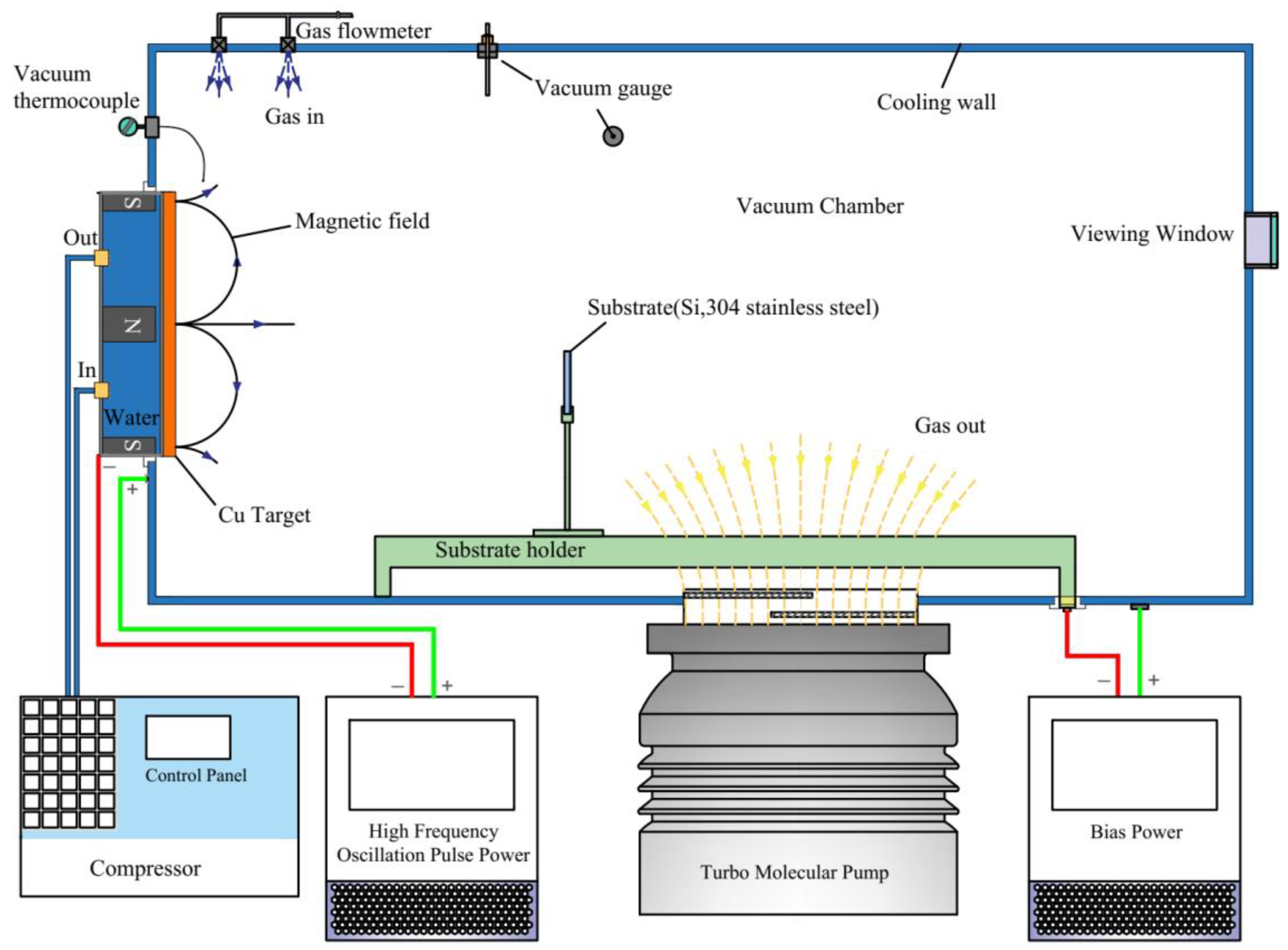
2.1. Deposition System

The homemade MAIP-001 (Xi’an University of Technology, Xi’an, China) magnetron sputtering system and oscillating pulse power supply were used for the experiment. The system was mainly composed of four parts: vacuum system, power system, control system, and cooling system.
The vacuum degree of the chamber with the water wall (700 × 400 × 350 mm3) was provided by the mechanical pump and the molecular pump. A cylindrical hollow structure with water-cooled magnetron on the back of the target (as shown in Figure 1) was adopted. The power supply system consists of an oscillating pulse power supply and a pulsed bias power supply. The maximum power of the oscillating pulse power supply is 8 kW, the maximum voltage is 1200 V, and the voltage oscillation frequency is 100 kHz, and the pulse width can be controlled in millisecond magnitude, which was loaded between the cathode target and the chamber as the power source for generating and maintaining plasma discharge. A pulsed bias power supply was loaded between the substrate and the chamber as the power source for triggering the ions to bombard the substrate. The amount and energy of the plasma bombardment substrate can be controlled by the bias electric field, so as to control the film deposition process. The pulsed bias voltage power supply has an arc extinguishing function, which can avoid the arcing phenomenon on the surface of the substrate or the workpiece, and reduce the damage of the arc to the substrate or the surface of the workpiece.

2.2. Deposition Process

The dimensions of the Cu target used for the oscillating pulse magnetron sputtering were Ø170 mm × 8 mm, and for the substrate material, ground and polished high-speed steel (W18Cr4V) and a P-type (100) Si sheet were selected. The size of the high-speed steels used to test the mechanical properties such as film–substrate adhesion was Ø45 mm × 4 mm, and of the rectangle Si sheet used for the detection of the microstructure of the film was 10 × 20 × 0.3 mm3.
Before the film deposition, the substrate was ultrasonically cleaned in anhydrous ethanol and acetone for 15 min, and then fixed on the workpiece holder in the vacuum chamber after drying. The distance between the substrate and the target was 240 mm. The substrate was parallel to the surface of the target, as shown in Figure 1.
The experimental parameters were formulated according to the volt–ampere characteristic curve of the Cu target, as shown in Figure 2. Obviously, when the target current was lower than 3 A, the current was almost proportional to the voltage. The target current was mainly composed of secondary electron flux (Ie), incident Ar+ flux (IAr+), and incident metal ion flux (ICu+). With the increase of the target current, the curve tended to be flat. The increment of the target current was represented by the thermal electron emission flux (Je), and the target current was changed from I1 = Ie + IAr+ + ICu+ to I2 = Ie + IAr+ + ICu+ + Je. Therefore, four groups of pure Cu films were prepared under the target currents of 2, 8, 13, and 18 A.
There were two stages for the deposition process: In Stage 1, Ar+ was used for 20 min of plasma cleaning of the substrate surface, and the substrate bias voltage was set at −450 V. Stage 2 was the deposition process of pure Cu films, with a substrate bias voltage set at −60 V, pulse width of the oscillating pulse electric field at 2 ms, duty cycle 20%, pulse discharge frequency 100 Hz, voltage oscillation frequency 100 kHz, voltage oscillation amplitude 50 V, and working pressure kept at 0.7 Pa.

2.3. Testing Equipment

A digital oscilloscope (DS2202, RIGOL Technologies, Dongguan, China) was used to measure the output waveform of the target power supply. A laser confocal microscope (LEXT OLS-4000, OLYMPUS Inc., Tokyo, Japan) was used to take photos of the target surface topography after the deposition process. A scanning electron microscope (SEM, JSM-6700F, JEOL Ltd., Tokyo, Japan) was used to observe the microstructure of the film, and the sampling process for the film section is shown in Figure 3. The crystal structure of the film was determined by an X-ray diffractometer (XRD, XRD-7000S, Shimadzu Limited Corp., Tokyo, Japan). The hardness and elastic modulus of films were measured by a nano-indenter (G200, KLA, Milpitas, CA, USA) with a selected pressing depth of about 1/8 of the film thickness. A Rockwell hardness tester was used to load 45 kg on the surface of the films and observe the indentation morphology, and the film–substrate adhesion was evaluated by the indentation morphology.

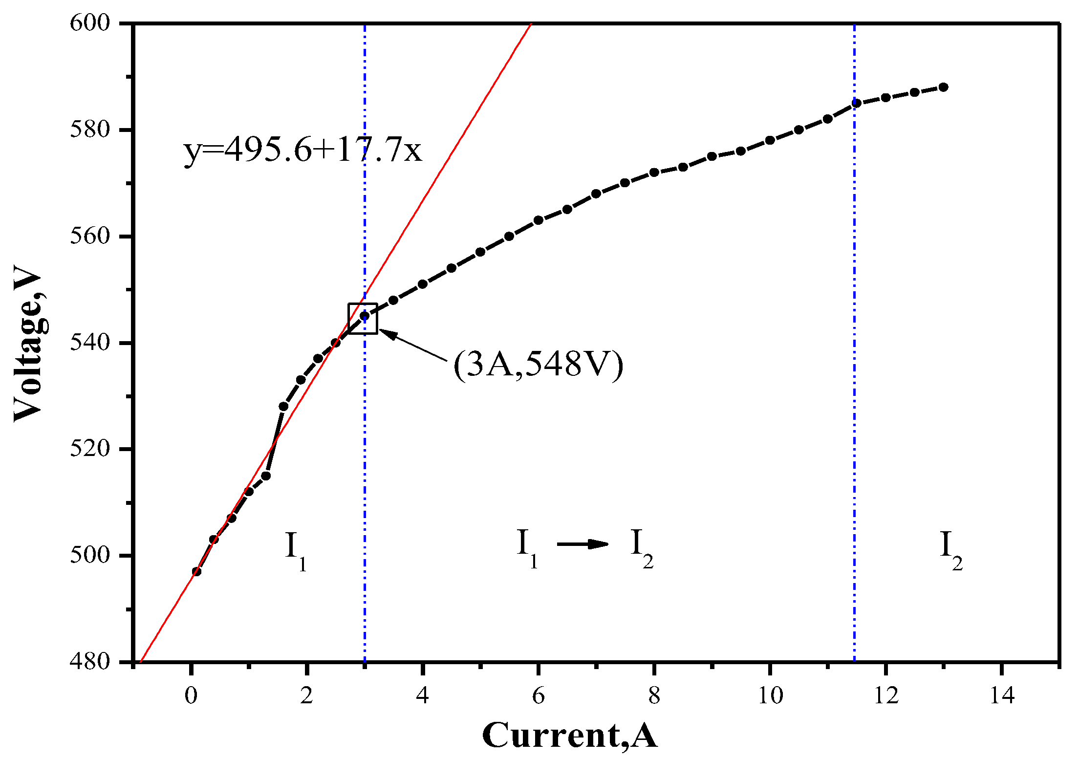
3. Oscillating Pulse Electric Field

Considering that plasma generation can be induced at lower voltage or power by the oscillating voltage technology [19], in this experiment, the oscillating pulse electric field was used to induce gas discharge on the target surface. A plasma power supply with voltage adjustable within 100–1000 V, a voltage oscillating frequency of 100 kHz, and pulse width controllable at the millisecond level was developed, based on the delayed response of the ionization/recombination period of argon atoms in argon gas to high-frequency switching of voltage between electrodes. With this power supply, a pulse electric field environment with a peak target current 10 times that of the conventional magnetron sputtering, a target current pulse width kept in a steady state at the millisecond level, and a target voltage with several microseconds of high-frequency oscillating was established between the magnetron cathode and the anode cavity wall, as shown in Figure 4. The voltage oscillates at a 100 kHz frequency, and Ar+ bombards the target surface at high frequency under the action of the electric field, making a large number of target atoms and secondary electrons escape from the target surface. Moreover, the pulse width at the ms level makes the target surface temperature higher than that of conventional HiPIMS, thus greatly advancing the thermal electron emission. The number of impact-ionized target metal ions increases with the number of secondary electrons, thermal electrons, and off-target atoms in the vacuum chamber, and the plasma density is higher than that of conventional HiPIMS. At the same time, the deposition rate is also greatly improved due to the longer discharge time. Therefore, the high plasma density and the rapid deposition of thin films are possible with OPMS technology at close to conventional DCMS target voltages.

4. Discussion

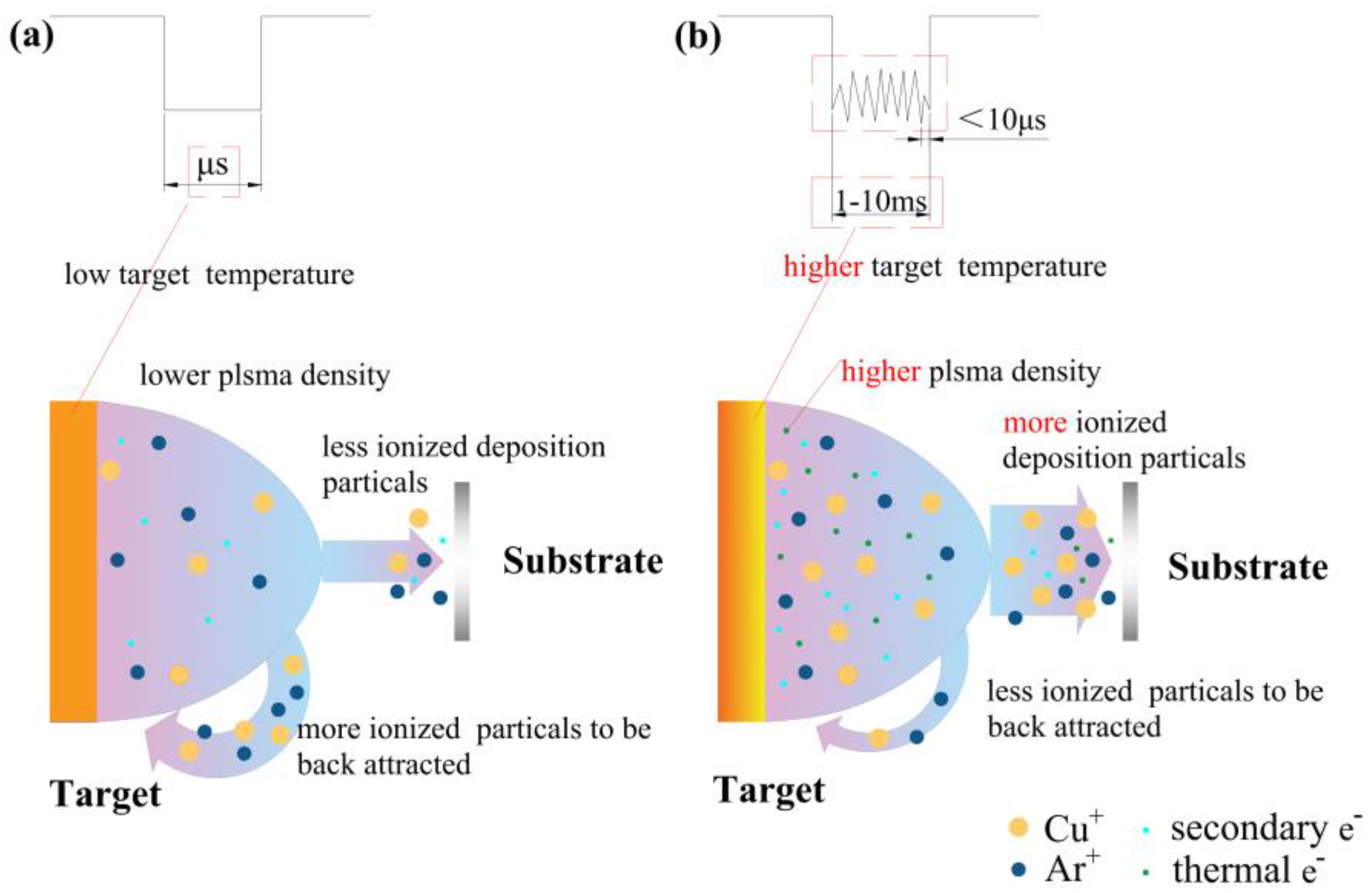
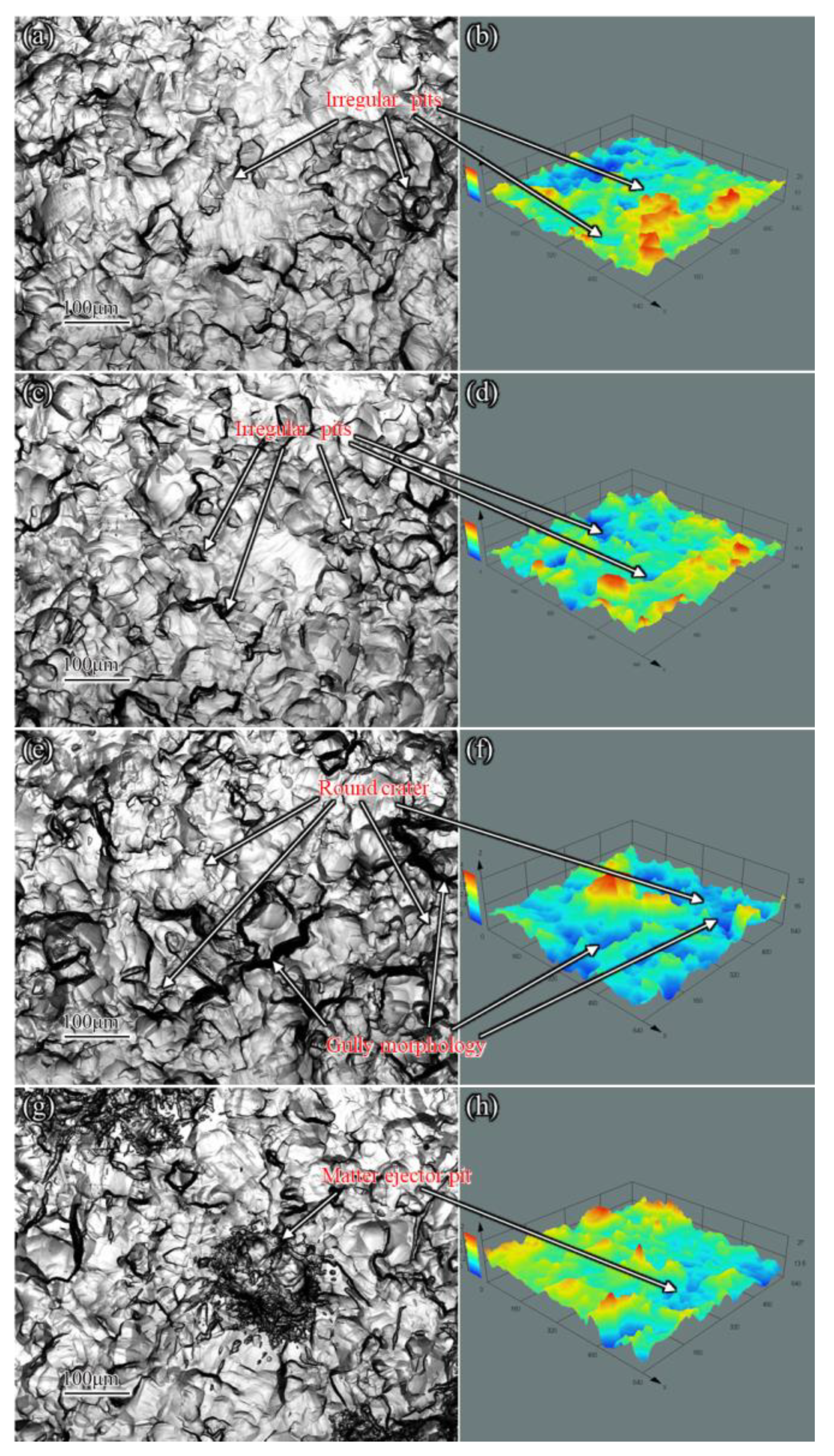
4.1. Surface Morphology of Target Material

The target surface morphology was obtained by laser scanning confocal microscopy (LSCM), as shown in Figure 5. When the target current was 2 A, the etched area of the target surface presented a large number of irregular pits. When the target current increased to 8 A, the quantity of Ar+ bombarding the target surface as well as the depth and size of pits on the target surface increased. When the target current was increased to 13 A, small circular melting pits (round crater) appeared on the target surface, indicating that the target surface material has undergone an evaporation or sublimation process. When the target current increased to 18 A, the material on the target surface showed an obvious materials ejection phenomenon (Figure 5g). This is consistent with the matter ejection model proposed by Martin et al. [20].
In conventional magnetron sputtering technology, the main way to remove the target materials is only sputtering [21]. The particles preferentially sputtered out of the target surface at low binding energy locations, such as grain boundaries, presenting an irregular pit morphology, as shown in Figure 5a. The number of sputtered particles depends on the number and kinetic energy of Ar+ bombarding the target surface, thus the number and kinetic energy of sputtered particles increased linearly with the target current. The number of deposition particles by sputtering as well as the size and number of pits on the target surface increased with the target current.
When the target current increased to 13 A, the number of secondary electrons escaping from the target surface obviously increased [22]. Since the electron work function at the grain boundary and defect microregion of the target surface was lower than that in the grain, the electron escape flux at the grain boundary and defect microregion was greater than that in the grain [23], resulting in obvious joule heat accumulation in the microregion of the target surface, and the generated heat can further increase the flux of electron escape; that is, the self-enhancement effect of electron escape occurred. This effect caused the target to evaporate in regions with low atomic binding energy, such as grain boundaries, so that a large number of atoms in this region were separated from the target surface, forming a round crater as shown in Figure 5e. At this point, the off-target method of deposition particles has changed into sputtering + evaporation. The number of off-target particles has no linear relation with the target current any more. In this unbalanced discharge mode, it is easy for the current density at the grain boundary to achieve the condition of arc generation.
With a further increase of the target current, an arc was formed on the target, the deposition particles in the grain boundary and other areas were melted and ejected, and the ejected material was left on the target surface as shown in Figure 5g. The bottom of the pits was filled by melted material as the ejection occurred at a defect such as a grain boundary, which decreased the pits’ depth, then the target surface was smooth and flat. At the same time, deposited particles containing molten droplets can reduce the film quality.
Therefore, when the target current was 13 A, sputtering + evaporation on the Cu target was an ideal off-target method before the ejection phenomenon occurred, which can not only avoid droplet formation, but also improve the ionization rate and the film deposition rate.

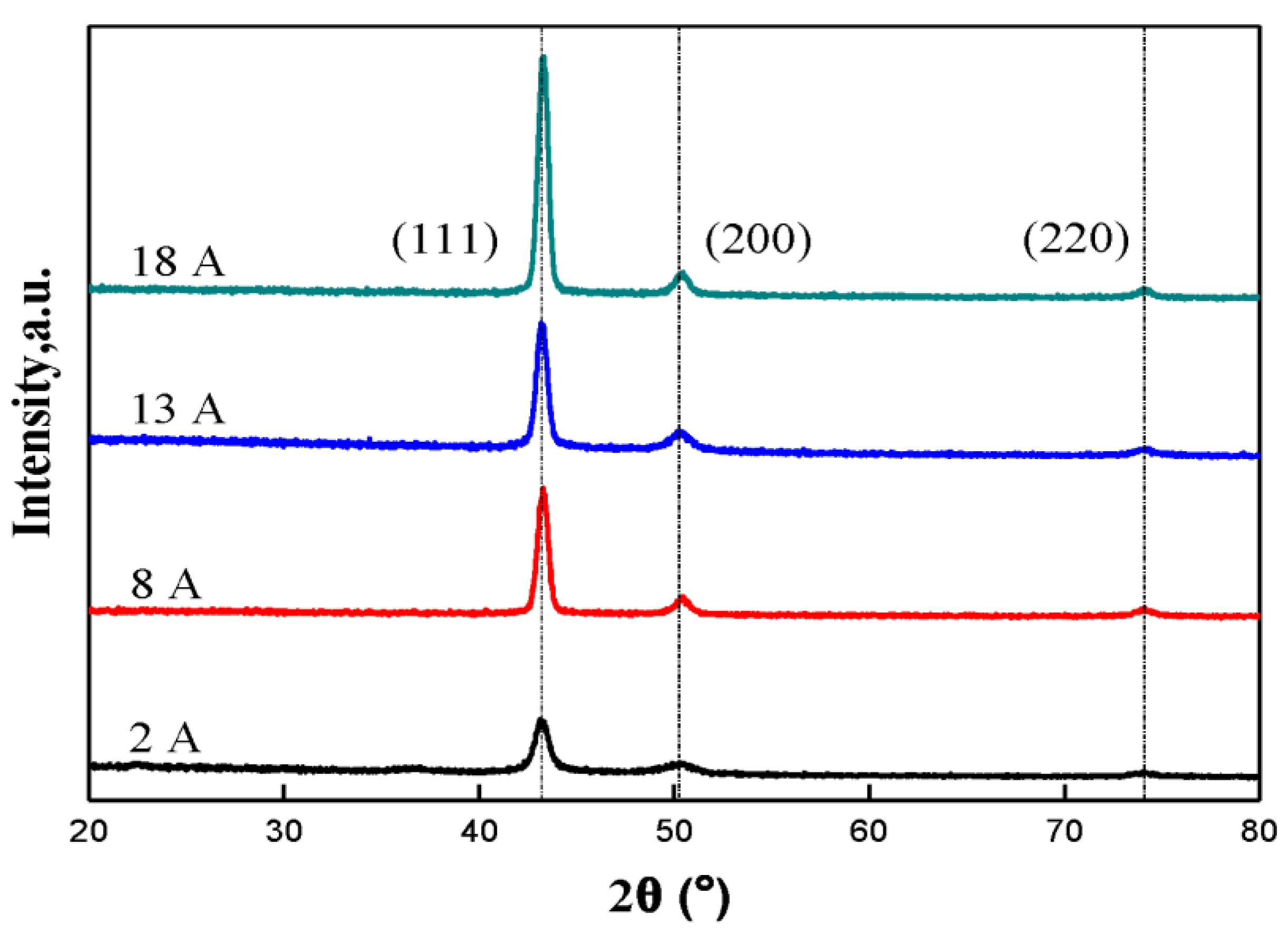
4.2. Crystal Structure
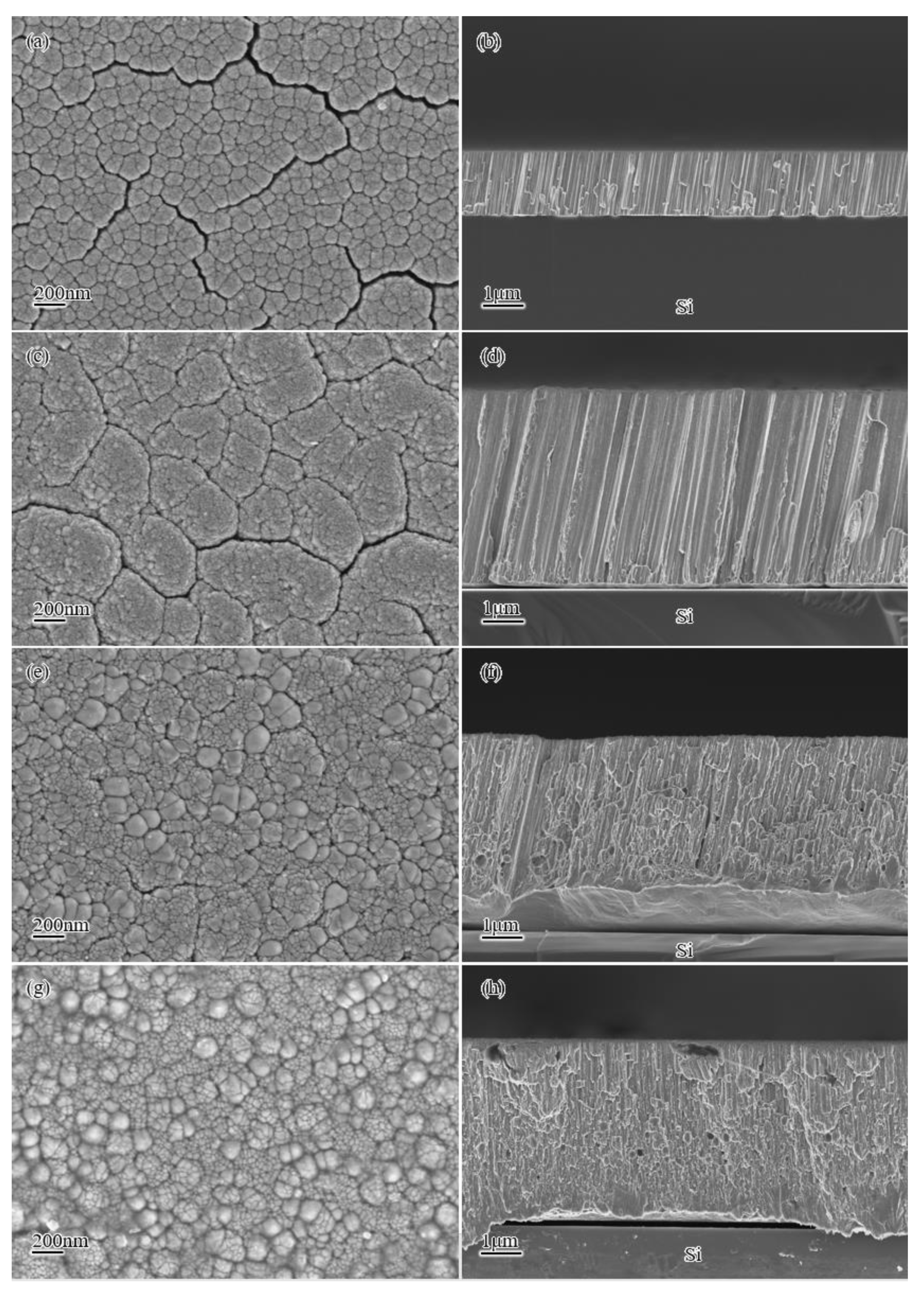
Figure 6 shows the XRD patterns of Cu samples under different peak currents. The four groups of samples had obvious diffraction peaks at 43°, 50°, and 74°. Compared with standard PDF card #89-2838, all samples were Cu films with a face-centered cubic (FCC) structure. Strong (111), weak (200), and (220) face-centered cubic Cu phases were detected for all of the samples.
Obviously, the difference in diffraction peak intensity indicated the differences in grain size and preferred orientation of the Cu film. The TC value was used to characterize the preferred orientation of the film [24,25]. The calculated results showed that for the four groups of samples, crystal plane (111) was preferentially oriented. The texture coefficient of crystal plane (111) increased gradually with the target current, indicating that the grain size of films grew to a certain extent. In the experiment, the Scherrer formula was used to calculate the average grain size of films [26] for further verification. As a result, the grain size of films increased with the target current, and the calculation results were as shown in Table 1.
When the target current was 2 A, crystal planes (111) and (200) were preferentially oriented for pure Cu films. When the target current increased from 8 to 18 A, the preferred orientation of films was dominated by crystal plane (111). It has been known that Cu with FCC structure owns crystal plane (111) with densely packed atoms, which has the lowest surface energy [27], while crystal plane (200) has the lowest strain energy [28]. Generally, the preferred orientation during film growth is the result of competition between strain energy and surface energy [29]. When the surface energy is dominant, crystal plane (111) is preferentially oriented, when the strain energy is dominant, crystal plane (200) is preferentially oriented, and if both are dominant, both crystal planes (111) and (200) are preferentially oriented.
The nucleation and growth of the film grains are mainly affected by the deposition conditions and the properties of the deposition particles. When the target current is small, the particles of collision sputtering off-target have a low ionization rate, the temperature rise of the substrate is not obvious during deposition, and thus, the free-energy difference of phase transition is increased, the critical nucleation size is decreased, and the grain size of the film is relatively small. At this point, due to the low diffusion energy of the deposition particles, both surface energy and strain energy dominate during the growth of films, and thus, crystal planes (111) and (200) are preferentially oriented. With the increase of the target current, the ionization rate of deposition particles was improved, and the deposition of ionized particles was accelerated under the bias electric field of the substrate. In this process, the temperature rise of the substrate was obvious, and thus, the free-energy difference in phase transition was reduced, and the critical nucleation size was increased.
According to the XRD patterns, the lattice constants (α) of the Cu film were calculated by using Cu (111) and (200) peaks. For all of the films, the lattice constant was larger than that of massive Cu (α = 3.613 Å). However, the films deposited by the sputtering + evaporation off-target method had lower α: 3.631 Å → 3.626 Å → 3.618 Å → 3.615 Å. In addition, the lattice parameters of the film were closer to those of bulk copper as the target current increased. Obviously, this variation of the lattice constant is related to the increase of the substrate temperature [30], as the temperature of the target surface and the characteristics of particles obtained from the target surface make the substrate obtain additional heat flux.

4.3. Microstructure

Figure 7 provides the SEM photos for the surface and section morphology of films. The surface morphologies for all of the four groups of Cu films were of round cell shape, and the size of these particles of round cell shape was increasing with the target current. When the target current was 2 A, there were cracks of about 50 nm-wide on the surface of the film. With the increase of the target current, the width of the cracks gradually decreased. These cracks and particles of round cell shape formed a cauliflower-like morphology (Figure 7a,c). When the current increased to 13 A, the cracks on the film surface tended to disappear, and at the same time, the particles of round cell shape with a diameter of about 100–150 nm appeared (Figure 7e), and the columnar structure of the section began to change into laminar morphology (Figure 7f). Moreover, the thickness of films was measured by the section topography. When the target current was 2, 8, 13, and 18 A, the thickness of the prepared films was 676, 1393, 1535, and 1691 nm, respectively.
The deposition of films was affected by factors such as temperature of deposition and properties of deposited particles [31], e.g., deposition quantity, deposition kinetic energy, etc., while the properties of deposited particles were influenced by the off-target method. Therefore, the growth and morphology of Cu films prepared under different off-target methods of deposition particles are different obviously. When the target current was 2 and 8 A, the main off-target method of deposited particles was sputtering, and both ionization rate and kinetic energy were relatively low. The deposited particles with a low ionization rate weakened the bombardment effect of plasma on the substrate. The substrate had a low deposition temperature, and the surface diffusion and volume diffusion of the particles deposited on the substrate were extremely low. According to the classical growth theory of film [32,33], the film grew in a fibrous or columnar form (Figure 4b). Additionally, the deposited particles with low ionization were affected by the shadow shielding effect during the deposition process, and thus, there were many cracks in the microstructure of films [34,35]. Due to the low energy carried by the off-target particles and the low deposition temperature of the film, it was difficult to release the internal stress of the film caused by lattice mismatch in the deposition process. With the increase of the film thickness, the internal stress superposition led to the cracking of the film at the defects such as grain boundaries.
When the target current increased to 13 A, the energy and ionization rate of deposited particles increased for the transformation of the off-target method, and under the bias electric field, the deposition of ions accelerated until the film formation of the substrate occurred. The high temperature of the target resulted in heat transfer of the deposited particles during the deposition process. With the increase of substrate temperature, affected by the deposition temperature, the stress in the film was released. When the target current increased to 18 A, it was difficult to observe cracks on the film surface, but the phenomenon of matter ejection occurred on the target surface, suggesting that some of the off-target particles were spherical molten droplets of large size, and some of the large molten droplets were deposited on the surface of the substrate, forming many unevenly distributed spherical particles, which greatly promoted the roughness of the film.
According to the section SEM images, the section morphology of the film was affected by the target current: when the target current was 2 and 8 A, the cross-section was at a certain angle with the substrate, showed a columnar morphology, and the interface between the Cu film and the Si substrate was well-bonded. With the increase of the target current, the orientation of the columnar structure was weakened until a compact structure with a few pores and defects was formed, with gaps appearing at the interface between the film and the substrate. When the target current was 13 and 18 A, obvious separation of the film from the substrate was observed. There were two reasons for this: (1) Copper and silicon have different thermal expansion coefficients. When the deposition temperature was high, the high temperature made the atoms in the film become fully diffused and the internal stress released, while for the film and the substrate themselves, the difference in crystal structure resulted in lattice mismatch and differences in thermal expansion coefficient between the two single-phase materials. After deposition, the stress produced in the process of temperature reduction was released at the interface between the two phases, and thus, the film was separated from the substrate. (2) In the film section sampling process, for the columnar structure formed under a low current, the crack propagation path was the gap parallel to the columnar structure, and therefore, the photos showed that the bond between the substrate and the film was strong. However, with the increase of the target current, the film became dense, and it became difficult for the cracks to penetrate the film. Thus, the cracks expanded at the gap between the film and the substrate, thus forming a more obvious gap. The film thickness was measured by the SEM image of the film section to obtain the deposition rate of the film, as shown in Table 1. The deposition rate of the film greatly increased with the target current, especially when the target current increased from 2 to 8 A, whereby the deposition rate increased by nearly 2.5 times. The average deposition rate of the film reached 102 nm/min when the target current was 18 A.

4.4. Mechanical Performance

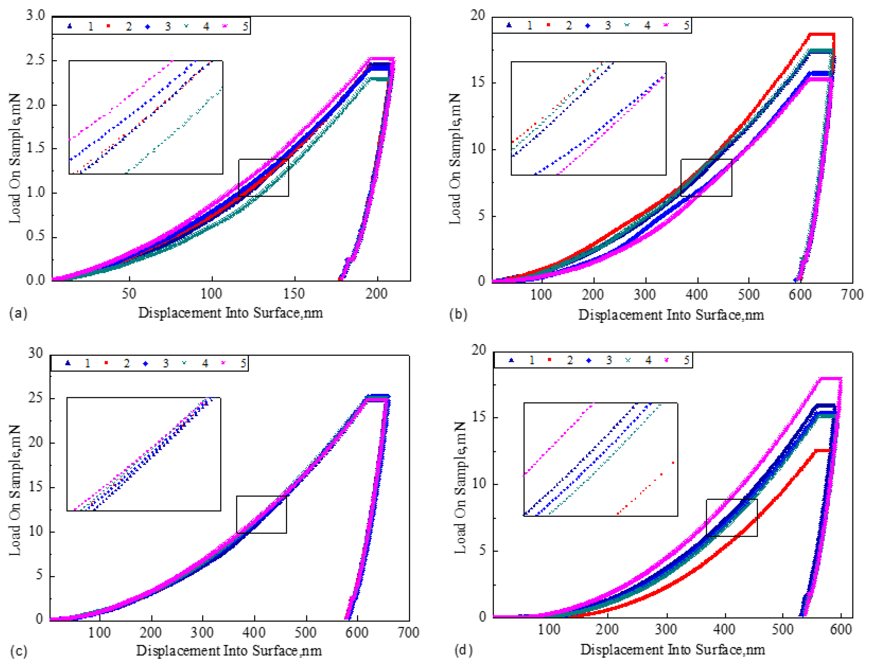
4.4.1. Hardness and Elastic Modulus

In this experiment, a nano-indenter was used to detect the hardness and elastic modulus under different peak current intensities, and five different points were selected for relevant measurement. The measured values were averaged.
Figure 8 shows the load displacement curves for four groups of pure Cu films. The load displacement curves for the films prepared at target currents of 2, 8, and 13 A had a high degree of coincidence, especially when the target current was 13 A, whereby the load displacement curves of the five points selected for the films almost completely coincided (see Figure 8c). However, the load displacement curves for the films deposited at the target current of 18A were not as good as those of the first three groups. When the target current increased from 2 to 13 A, due to the temperature rise of the target surface, the off-target method of deposited particles changed from sputtering to sputtering + evaporation, which dramatically increased the number of off-target atoms. Thus, the number of copper ions in the vacuum chamber dramatically increased when the probability of collision ionization increased. The ions deposited into the substrate had both high internal energy and high kinetic energy under the influence of bias acceleration and target temperature, and thus, their diffusion ability on the substrate surface was increased. For this, with the increase of the target current, the compactness of the film was effectively improved. Therefore, at 13 A, as the nano-indenter was indented, the compactness and structure, as well as the mean contact compressive stress during the plastic deformation, were all the same for the positions. When the current increased to 18 A, the inclusion of molten droplets in the deposited particles, which caused the abnormal growth of grains at their deposition sites. As a result, the hardness distribution of the film was uneven, and the load–displacement curve was relatively discrete.
According to Table 1, when the target current was 13 A, the hardness of the Cu film was at a maximum. When the target current increased to 18 A, a material ejection phenomenon appeared on the target surface. There were molten droplets in the deposited particles, which were difficult to be ionized, although the film was compact. At the same time, the high deposition temperature caused abnormal grain growth. The above reasons led to the decrease of hardness and elastic modulus of the films. When the current was 2 A, the grain size of the prepared film was 13.4 nm. The H/E value of the Cu thin film was much less than 0.1, and the plastic deformation of the thin film was dominant. Meanwhile, the plastic deformation resistance of the films was the best among the four groups of samples. In addition, the film deposited at a target current of 13 A has the highest hardness and the most uniform distribution of mechanical properties.

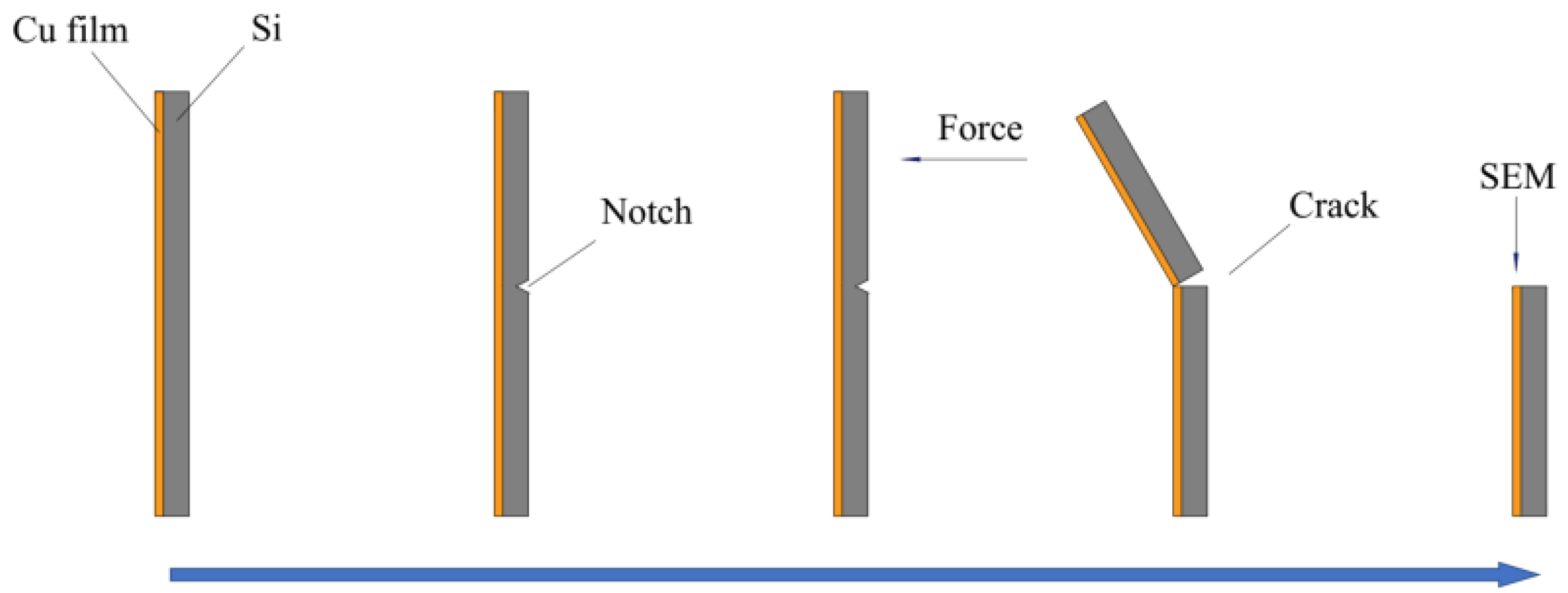
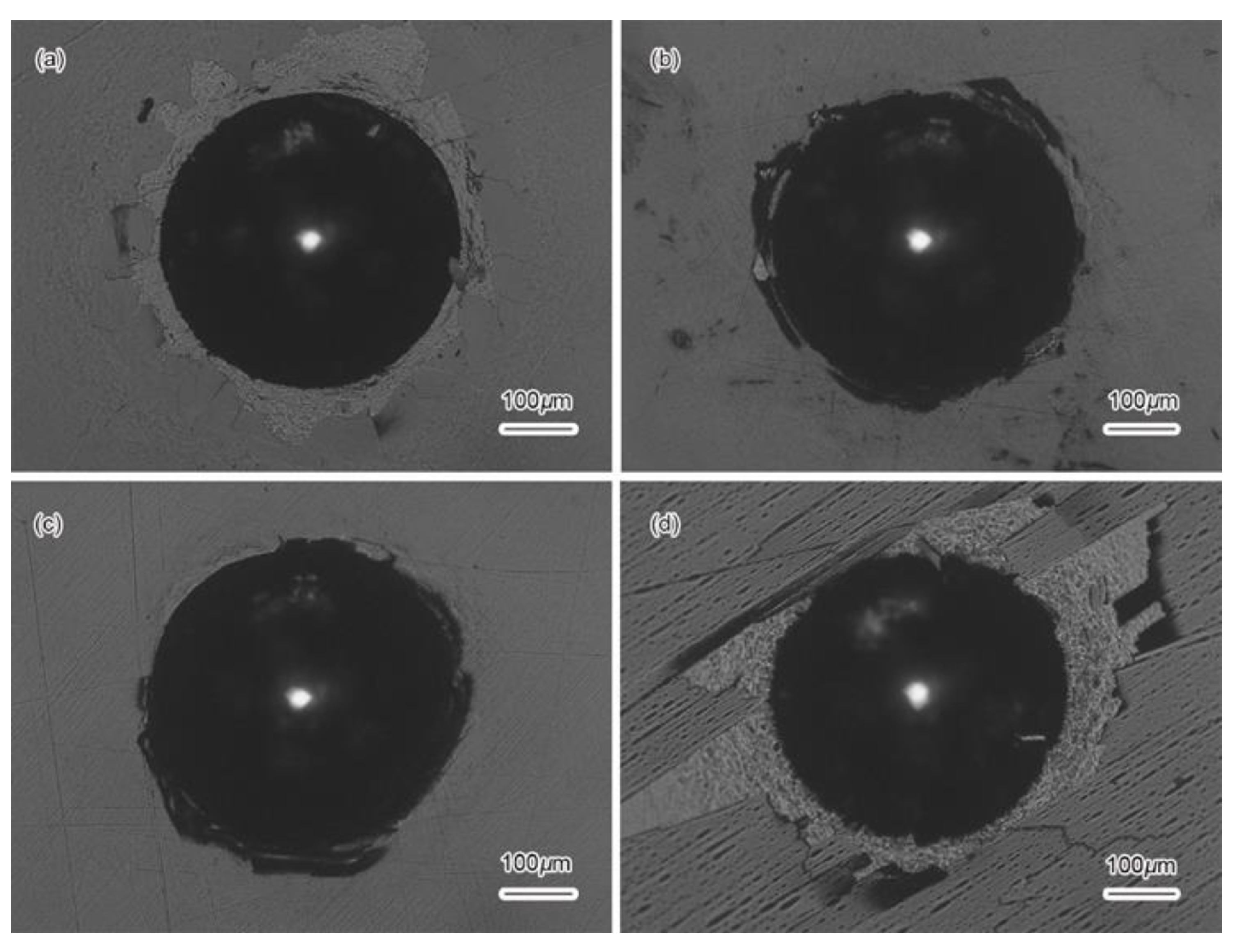
4.4.2. Film–Substrate Adhesion

In the experiment, the Rockwell indentation method was used to evaluate the film–substrate adhesion of films. The indentation morphology is shown in Figure 9. Films deposited at a target current of 2 A had less cracking and spalling around the indentation. When the target current was 8 and 13 A, there were almost no cracks around the films’ indentation, and only a small number of films fell off, indicating that the film had a strong film–substrate adhesion. When the target current was 18 A, the films cracks were the most obvious, and the film–substrate adhesion was the worst at this time.
The main factors influencing the adhesion are films’ thickness, microstructure, mechanical performance, and residual stress [36,37,38]. Generally, high film density, good mechanical performance, and low residual stress are beneficial to relieve the cracking of the coating under load and improve the adhesion of the films. The indentation morphologies of the four groups of films were observed, and it was found that the coatings prepared when the target current was 2 A had a small thickness and a loose structure, and the lattice mismatch caused by the low activity of the deposited particles during film formation increased the residual stress of the films [39,40]. Therefore, the films showed poor adhesion.
With the increase of the target current, the off-target method of deposited particles gradually became sputtering + evaporation. Thicker films were prepared in the same deposition time, the film structure was denser, and the residual stress was reduced, which was beneficial to the improvement of film–substrate adhesion. However, as the target current increased to 18 A, the film–substrate adhesion strength decreased, and obvious film cracking and peeling were observed (Figure 9d). The reason is that the atoms in the film were sufficiently diffused when the deposition temperature increased. After the deposition, the substrate temperature decreased, and there was a large internal stress between the film and the substrate due to the different thermal expansion coefficients. When the Rockwell indenter was pressed into the film, the internal stress was released along the bonding interface between the film and the substrate, and then obvious damage and peeling occurred.

5. Conclusions

In this experiment, oscillating pulsed magnetron sputtering was used to deposit pure Cu films at different peak target currents.
As the target current increased, the off-target method of the deposited particles changed from sputtering to sputtering + evaporation. When the target current reached 18 A, a materials ejection phenomenon appeared on the surface of the target.
With the increase of the peak current, the grain size of the film slightly increased. When the peak current was more than 8 A, the deposition rate of the film significantly increased, and when the target current was 13 A, the off-target method of deposited particles became sputtering + evaporation. At this point, the deposition rate was as high (the actual deposition rate was 84.9 nm/min, and the deposition rate per unit power was 2.79 μm/(h·kW)) as nearly four times that of conventional HiPIMS, and furthermore, the film structure was dense, the stress–strain curves measured at five points of the film almost overlapped, the hardness reached 2.61 GPa, and the film–substrate adhesion strength was the best among the four groups. When the peak current reached 18 A, although the deposition rate was extremely high, the properties of the films severely deteriorated due to the inclusion of molten droplets in the deposited particles.

Author Contributions

Conceptualization, B.J. and C.Y.; investigation, F.Y. and J.S.; data curation, N.Z.; writing—original draft preparation, R.W.; supervision, J.H.; methodology, C.Y. and W.S.; funding acquisition, B.J. All authors have read and agreed to the published version of the manuscript.

Funding

This research was funded by National Natural Science Foundation of the Republic of China; funding number, 52001251; Funder, C.Y.

Institutional Review Board Statement

Not applicable.

Informed Consent Statement

Not applicable.

Data Availability Statement

Not applicable.

Acknowledgments

Thanks to B.J. for his guidance and experimental equipment support. Thanks to C.Y. for his revisions and suggestions on this paper.

Conflicts of Interest

The authors declare no conflict of interest.

References

  1. Li, J.; Zhang, H.; Fan, A.; Tang, B. Tribological properties characterization of Ti/Cu/N thin films prepared by DC magnetron sputtering on titanium alloy. Surf. Coat. Technol. 2016, 294, 30. [Google Scholar] [CrossRef]
  2. Le, M.T.; Sohn, Y.U.; Lim, J.W.; Choi, G.S. Effect of sputtering power on the nucleation and growth of Cu films deposited by magnetron sputtering. Mater. Trans. 2010, 51, 116–120. [Google Scholar] [CrossRef] [Green Version]
  3. Zhu, B.L.; Yi, C.H.; Zhao, X.; Ma, J.M.; Wu, J.; Shi, X.W. Improvement of transparent conductive properties of Cu films by introducing H2 into deposition atmosphere during RF magnetron sputtering. Superlattices Microstruct. 2020, 145, 106628. [Google Scholar] [CrossRef]
  4. Naghdi, S.; Rhee, K.Y.; Hui, D.; Park, S.J. A review of conductive metal nanomaterials as conductive, transparent, and flexible coatings, thin films, and conductive fillers: Different deposition methods and applications. Coatings 2018, 8, 278. [Google Scholar] [CrossRef] [Green Version]
  5. Sarakinos, K.; Alami, J.; Konstantinidis, S. High power pulsed magnetron sputtering: A review on scientific and engineering state of theart. Surf. Coat. Technol. 2010, 204, 1661. [Google Scholar] [CrossRef]
  6. Kouznetsov, V.; Macák, K.; Schneider, J.M.; Helmersson, U.; Petrov, I. A novel pulsed magnetron sputter technique utilizing very high target power densities. Surf. Coat. Technol. 1999, 122, 290. [Google Scholar] [CrossRef]
  7. Li, C.W.; Tian, X.B. Novel high power impulse magnetron sputtering enhanced by an auxiliary electrical field. Rev. Sci. Instrum. 2016, 87, 083507. [Google Scholar] [CrossRef] [PubMed]
  8. Lin, J.; Moore, J.J.; Sproul, W.D.; Mishra, B.; Wu, Z.; Wang, J. The structure and properties of chromium nitride coatings deposited using dc, pulsed dc and modulated pulse power magnetron sputtering. Surf. Coat. Technol. 2010, 204, 2230. [Google Scholar] [CrossRef]
  9. Aiempanakit, M.; Kubart, T.; Larsson, P.; Sarakinos, K.; Jensen, J.; Helmersson, U. Hysteresis and process stability in reactive high power impulse magnetron sputtering of metal oxides. Thin Solid Films 2011, 519, 7779. [Google Scholar] [CrossRef] [Green Version]
  10. Anders, A. Deposition rates of high power impulse magnetron sputtering: Physics and economics. J. Vac. Sci. Technol. 2010, 28A, 783. [Google Scholar] [CrossRef] [Green Version]
  11. Brenning, N.; Huo, C.; Lundin, D.; Raadu, M.A.; Vitelaru, C.; Stancu, G.D.; Minea, T.; Helmersson, U. Understanding depositionrate loss in high power impulse magnetron sputtering: I. Ionizationdriven electric fields. Plasma Sources Sci. Technol. 2012, 21, 025005. [Google Scholar] [CrossRef] [Green Version]
  12. Lu, C.Y.; Diyatmika, W.; Lou, B.S.; Lu, Y.C.; Duh, J.G.; Lee, J.W. Influences of target poisoning on the mechanical properties of TiCrBN thin films grown by a superimposed high power impulse and medium-frequency magnetron sputtering. Surf. Coat. Technol. 2017, 32, 86–95. [Google Scholar] [CrossRef]
  13. Luo, Q.; Yang, S.; Cooke, K.E. Hybrid HIPIMS and DC magnetron sputtering deposition of TiN coatings: Deposition rate, structure and tribological properties. Surf. Coat. Technol. 2013, 236, 13. [Google Scholar] [CrossRef]
  14. Stranak, V.; Drache, S.; Bogdanowicz, R.; Wulff, H.; Herrendorf, A.P.; Cada, M.; Tichy, M.; Hippler, R. Effect of midfrequency discharge assistance on dual-high power impulse magnetron sputtering. Surf. Coat. Technol. 2012, 206, 2801. [Google Scholar] [CrossRef]
  15. Bleykher, G.A.; Krivobokov, V.P.; Yurjeva, A.V.; Sadykova, I. Energy and substance transfer in magnetron sputtering systems with liquid-phase target. Vacuum 2016, 124, 11–17. [Google Scholar] [CrossRef]
  16. Yuryeva, A.V.; Shabunin, A.S.; Korzhenko, D.V.; Korneva, O.S.; Nikolaev, M.V. Effect of material of the crucible on operation of magnetron sputtering system with liquid-phase target. Vacuum 2017, 141, 135–138. [Google Scholar] [CrossRef]
  17. Getty, S.A.; Auciello, O.; Sumant, A.V.; Dutta, A.K.; Wang, X.; Glavin, D.P.; Mahaffy, P.R. Characterization of nitrogen-incorporated ultrananocrystalline diamond as a robust cold cathode material. In Proceedings of the Micro and Nanotechnology Sensors, Systems, and Applications-II, Orlando, FL, USA, 5 April 2010; p. 76791N. [Google Scholar] [CrossRef]
  18. Harniman, R.; May, P.W.; Fox, O. Direct observation of electron emission from CVD diamond grain boundaries by tunnelling atomic force microscopy independent of surface morphology. Diam. Relat. Mater. 2017, 80, 147–152. [Google Scholar] [CrossRef]
  19. Audronis, M.; Kelly, P.J.; Arnell, R.D.; Valiulis, A.V. Pulsed magnetron sputtering of chromium boride films from loose power targets. Surf. Coat. Technol. 2006, 200, 4166–4173. [Google Scholar] [CrossRef]
  20. Martin, P.; McKenzie, D.; Netterfield, R.; Swift, P.; Filipczuk, S.; Müller, K.; Pacey, C.; James, B. Characteristics of titanium arc evaporation processes. Thin Solid Films 1987, 153, 91–102. [Google Scholar] [CrossRef]
  21. Kelly, P.J.; Arnell, R.D. Magnetron sputtering: A review of recent developments and applications. Vacuum 2000, 56, 159. [Google Scholar] [CrossRef]
  22. Magnus, F.; Sveinsson, O.B.; Olafsson, S.; Gudmundsson, J.T. Current-voltage-time characteristics of the reactive Ar/N2 high power impulse magnetron sputtering discharge. J. Appl. Phys. 2011, 110, 83306. [Google Scholar] [CrossRef]
  23. Karabutov, A.V.; Frolov, V.D.; Pimenov, S.M.; Konov, V.I. Grain boundary field electron emission from CVD diamond coatings. Diam. Relat. Mater. 1999, 8, 763–767. [Google Scholar] [CrossRef]
  24. Fujimura, N.; Nishihara, T.; Goto, S.; Xu, J.; Ito, T. Control of preferred orientation for ZnOx films: Control of self-texture. J. Cryst. Growth 1993, 130, 269–279. [Google Scholar] [CrossRef]
  25. Gu, M.; Yang, F.Z.; Huang, L. XRD study on highly preferred orientation Cu electrodeposit. Electrochemistry 2002, 8, 282–287. [Google Scholar]
  26. Patterson, A.L. The Scherrer formula for X-ray particle size determination. Phys. Rev. 1939, 56, 978. [Google Scholar] [CrossRef]
  27. Zhang, J.; Xu, K.; Zhang, M. Theory of abnormal grain growth in thin films and analysis of energy anisotropy. Acta. Phys. Sin. 2003, 52, 1207. [Google Scholar] [CrossRef]
  28. Zhang, J.M.; Xu, K.W. Dependence of strain-energy density on the grain orientation in fcc-polycrystalline films. Acta. Phys. Sin. 2002, 51, 2562. [Google Scholar]
  29. Yeh, T.S.; Wu, J.M.; Hu, J.M. The properties of TiN thin films deposited by pulsed direct current magnetron sputtering. Thin Solid Films 2008, 516, 7294. [Google Scholar] [CrossRef]
  30. Sandström, P.; Svedberg, E.B.; Birch, J.; Sundgren, J.-E. Structure and surface morphology of epitaxial Ni films grown on MgO(111) substrates: Growth of high quality single domain films. J. Cryst. Growth 1999, 197, 849–857. [Google Scholar] [CrossRef]
  31. Zheng, W.T. Thin Film Materials and Thin Film Technology; Chemical Industry Press: Beijing, China, 2008; pp. 66–167. [Google Scholar]
  32. Petrov, I.; Barna, P.B.; Hultman, L.; Greene, J.E. Microstructural evolution during film growth. J. Vac. Sci. Technol. A Vacuum Surfaces Films 2003, 21, S117–S128. [Google Scholar] [CrossRef]
  33. Ueng, H.Y.; Guo, C.T.; Dittrich, K.H. Development of a hybrid coating process for deposition of diamond like carbon films on microdrills. Surf. Coat. Technol. 2006, 200, 2900. [Google Scholar] [CrossRef]
  34. Yao, S.K. Theoretical model of thin-film deposition profile with shadow effect. J. Appl. Phys. 1979, 50, 3390. [Google Scholar] [CrossRef]
  35. Mukherjee, S.; Gall, D. Structure zone model for extreme shadowing conditions. Thin Solid Films 2013, 527, 158. [Google Scholar] [CrossRef]
  36. Kim, T.H.; Lee, S.J.; Kim, D.H.; Kim, D.W.; Bae, J.W.; Kim, K.N.; Kim, Y.M.; Yeom, G.Y. Residual stress control of Cu film deposited using a pulsed direct current magnetron sputtering. Thin Solid Films 2018, 660, 601–605. [Google Scholar] [CrossRef]
  37. Qin, W.; Chen, M.; Wang, Y.; Jiang, Y. Structures and adhesion of hcp thin film coating interfaces on a single-crystal bcc substrate by PVD: Ti/Mo and Zr/Mo. Comput. Mater. Sci. 2020, 174, 109504. [Google Scholar] [CrossRef]
  38. Shtern, M.Y.; Karavaev, I.S.; Shtern, Y.I.; Kozlov, A.O.; Rogachev, M.S. The surface preparation of thermoelectric materials for deposition of thin-film contact systems. Semiconductors 2019, 53, 1848–1852. [Google Scholar] [CrossRef]
  39. Aissa, K.A.; Achour, A.; Camus, J.; Le Brizoual, L.; Jouan, P.-Y.; Djouadi, M.-A. Comparison of the structural properties and residual stress of AlN films deposited by dc magnetron sputtering and high power impulse magnetron sputtering at different working pressures. Thin Solid Films 2014, 550, 264–267. [Google Scholar] [CrossRef]
  40. Zhang, Y.-Z.; Zhang, S.-R.; Yu, D.-B.; Luo, Y.; Quan, N.-T.; Yan, W.-L.; Li, K.-S. Structural properties and crystal orientation of polycrystalline Gd films. Rare Met. 2017. [Google Scholar] [CrossRef]
Figure 1. Schematic diagram of the MAIP-001 deposition system.
Coatings 12 00394 g001
Figure 2. The gas volt–ampere characteristic curve of the copper target.
Coatings 12 00394 g002
Figure 3. Coating cross-section sampling process for SEM observation.
Coatings 12 00394 g003
Figure 4. Schematics of the discharge mechanism: (a) conventional HiPIMS and (b) oscillating pulse magnetron sputtering (OPMS).
Coatings 12 00394 g004
Figure 5. 2D and 3D microscopic topography of Cu target surface under different currents: (a,b) 2 A, (c,d) 8 A, (e,f) 13 A, and (g,h) 18 A.
Coatings 12 00394 g005
Figure 6. XRD pattern of the Cu coatings.
Coatings 12 00394 g006
Figure 7. Surface and cross-section morphology of Cu films at different peak currents: (a,b) 2 A, (c,d) 8 A, (e,f) 13 A, and (g,h) 18 A.
Coatings 12 00394 g007
Figure 8. Load–displacement curve of Cu film under different peak currents: (a) 2 A, (b) 8 A, (c) 13 A, and (d) 18 A.
Coatings 12 00394 g008
Figure 9. Indentation morphologies of Cu films: (a) 2 A, (b) 8 A, (c) 13 A, and (d) 18 A.
Coatings 12 00394 g009
Table 1. Experimental results of the Cu coatings deposited at different target currents 1.
Sample IDI (A)G (nm)V (nm/min)H (GPa)E (GPa)Preferred Orientationα (Å)
1213 ± 0.632 d18.23 ± 0.089 d2.44 ± 0.053 a132.17 ± 4.858 d(111) and (200)3.631 ± 0.012 a
2815 ± 1.095 c66.40 ± 0.095 c1.69 ± 0.066 a136.38 ± 7.687 c(111)3.626 ± 0.031 a
31316 ± 0.894 b84.85 ± 0.071 b2.61 ± 0.077 a154.10 ± 8.665 b(111)3.618 ± 0.012 a
41818 ± 0.632 a102.47 ± 0.120 a1.92 ± 0.078 a156.20 ± 5.593 a(111)3.615 ± 0.011 a
I—peak current; G—grain size; V—deposition rate; H—hardness; E—elastic modulus; α—lattice constant. 1 Results are reported as the mean ± standard deviation. Different lowercase letters within each column indicate significant statistical differences (p < 0.05) between films.
Publisher’s Note: MDPI stays neutral with regard to jurisdictional claims in published maps and institutional affiliations.

