1. Introduction
Solar energy plays an increasingly important role as a clean energy source [
1]. In order to meet the global demand for energy, different types of solar cells have been developed—amorphous silicon cells [
2], single crystalline silicon cells [
3], gallium arsenide cells [
4], and perovskite cells [
5,
6,
7], among others. Silicon solar cells offer the advantages of long life, reliable performance, low price, and extensive applications in the photovoltaic field [
8,
9]. In recent years, micro-nano structures such as microlens arrays (MLAs) [
10,
11], inverted pyramid [
12,
13], nanowires [
14], nano-gratings [
15], micro/nanocones, and bionics [
16], have been built on the surface of silicon solar cell devices to improve photoelectric conversion efficiency.
Among all the micro-nano structures, MLAs have been widely applied to improve the quality of solar cell devices. For example, Lin et al. reported a circular lens in epoxy polymer state to enhance the power conversion efficiency (PCE) of silicon solar cell devices, resulting in output power improvement by about 8.6% [
17]. Ha et al. prepared a dye-sensitized solar cell device with a polymer lens, improving the maximum output power by about 50.2% [
18]. Tseng et al. proposed an optical film with a cylindrical MLAs structure, increasing PCE by 3.3% [
19]. Li et al. applied nanoscale nipple arrays deposited on the surface of cylindrical lens arrays to solar cell devices and reported PCE increase by 4.95% [
20]. The above studies show that MLAs have broad prospects and extremely high popularity in improving the quality of solar cells.
In this paper, different MLAs were constructed on organic–inorganic hybrid film surfaces using UV nanoimprint technology. The hybrid film MLAs were then attached to silicon solar cell devices. In addition, the optical and structural features of both the hybrid films and the MLAs were studied. At the same time, the hydrophobic and diffraction properties of the MLAs were also characterized. Finally, photovoltaic performances, including the current voltage and power of the silicon solar cells with hybrid film MLAs were investigated. It was revealed that the PCE of silicon solar cell device with circular MLAs increased by a maximum of 10.48%. It should be emphasized that the improvement here refers to a relative percentage gain. Thus, we have shown a concise and effective method for organic–inorganic hybrid film MLAs to be applied to silicon solar cells.
2. Materials and Methods
2.1. Design of MLAs Masks
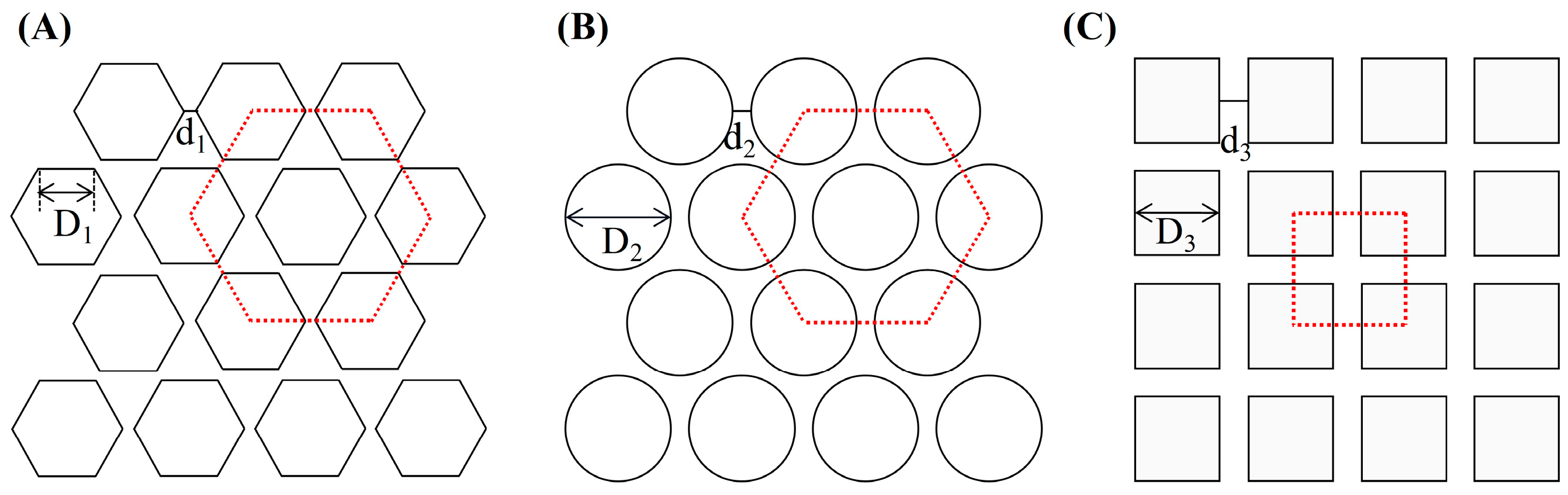
Figure 1 describes the design of MLAs masks. It can be seen that circular and hexagonal MLAs are designed as a honeycomb shape, and the square MLAs are designed as a square shape. D
1 and D
3 are the side lengths of the MLAs, D
2 is the diameter, and d
1, d
2, and d
3 represent the pitch. It should be emphasized that the distance between two pattern centers of the MLAs are 65, 42, and 45 µm for the hexagonal, circular, and square MLAs, respectively. The values of the detailed parameters, including the diameter and space of the MLAs, can be found in
Table 1.
2.2. Fabrication Process of Hybrid Film MLAs Built on Silicon Solar Cells
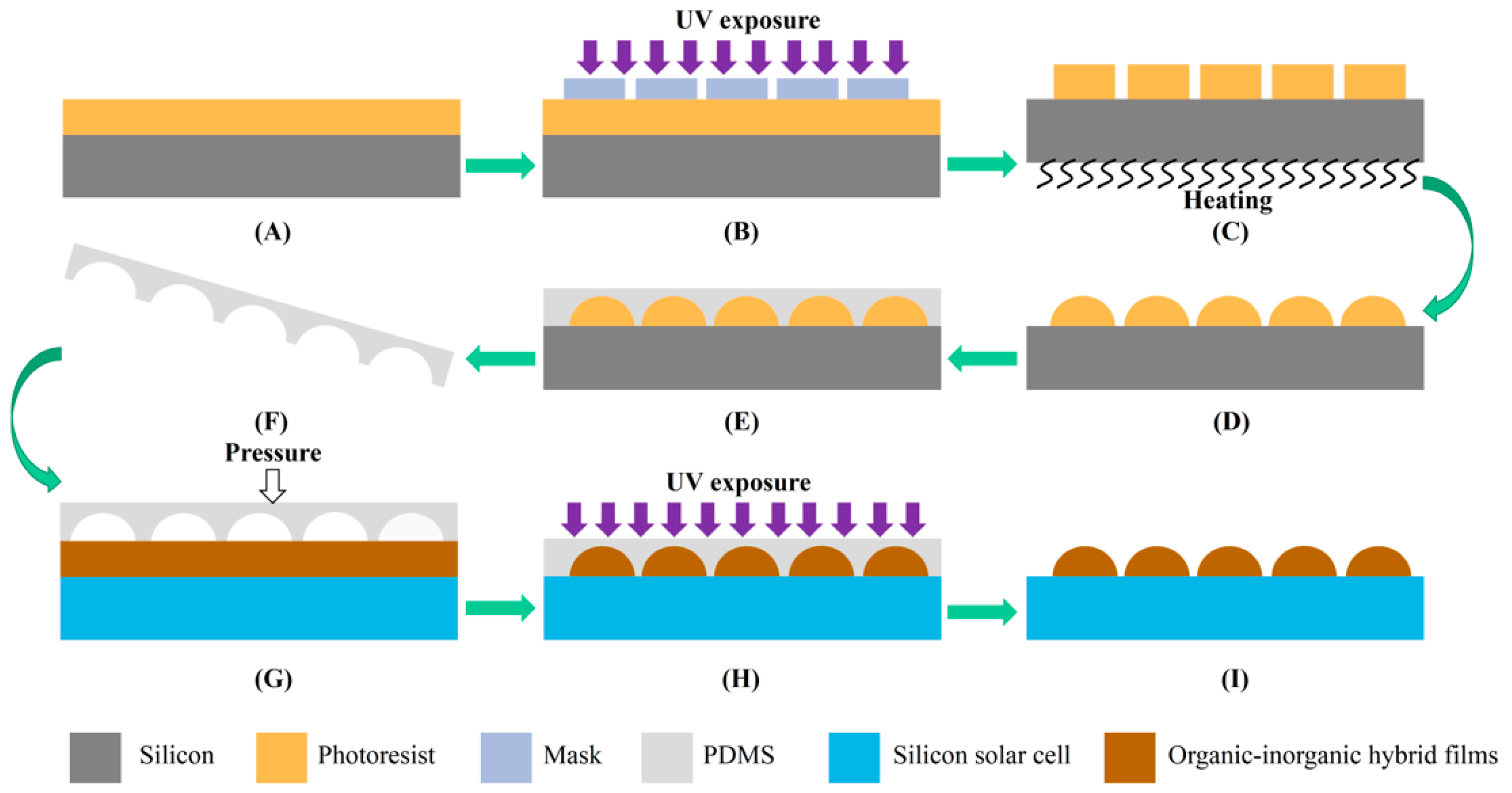
The flowchart of the fabrication procedure of the hybrid film MLAs built on silicon solar cells is shown in
Figure 2. There are mainly two steps: First, the original MLAs templates were prepared by combining photolithography and photoresist thermal reflow method, as shown in
Figure 2A–D. Second, the organic–inorganic hybrid film MLAs were prepared on silicon solar cells by using the ultraviolet nano-imprint technique, as shown in
Figure 2E–H. The detailed fabrication process is provided below.
2.3. Preparation Process of Organic–Inorganic Hybrid Films
This process mainly includes the preparation process of three mixed solutions. Solution I: 4 mol of ethanol was mixed with 1 mol of 3-glycidoxypropyltrimethoxysilane (GLYMO), 4 mol of deionized water, and 0.05 mol of hydrochloric acid; the liquid mixture was stirred continuously for 60 min. Solution II: 4 mol of acetylacetone was dissolved in 1 mol of tetrabutyl titanate (TPOT); the liquid mixture was then stirred continuously for 60 min. Solution III: 4 mol of deionized water was mixed in 1 mol of 3-methacryloxypropyltrimethoxysilane (MEMO), 4 mol of isopropyl alcohol, and 0.05 mol of hydrochloric acid, and then stirred continuously for 60 min. The three solutions were mixed at a certain molar ratio—TPOT: GLYMO: MEMO = 0.3: 0.2: 0.2. Finally, the liquid mixture was placed at 25 °C and stirred continuously for 48 h; this was done to allow the solution to fully dissolve and react. It should be mentioned that 2,4,6-trimethylphenyl with 3 wt.% was added as a photo-initiator in the above liquid mixture half an hour before the solution was used. Organic–inorganic hybrid films were then prepared on silicon solar cells or a glass surface using the spin coating technique at 1800 rpm for 1 min. The thickness of the films was measured to be about 10 µm.
2.4. Preparation of the MLAs Templates
The MLAs templates were prepared by using photolithography and photoresist thermal reflow methods, as shown in
Figure 2A–D. First, photoresist (AZ-1500) films were spin-coated on a clean silicon substrate surface at 1500 rpm for 1 min. Second, the photoresist film was baked at 100 °C in an oven for 10 min to remove excess moisture and solvents. Third, the photoresist film samples were placed under UV light for 1 min using a Ge mask. After treatment with the alcohol solution, the photoresist sample was placed on a hot plate at 150 °C for 60 min. Finally, photoresist templates with MLAs were fabricated.
2.5. Hybrid Film MLAs Built on Silicon Solar Cells
The organic–inorganic hybrid film MLAs were fabricated on silicon solar cells with the ultraviolet imprint technique, as shown in
Figure 2E–I. At first, a PDMS monomer (Sylgard 184) and cured adhesive were mixed at a mass ratio of 10:1 in a small beaker. The mixture was slowly placed on the MLAs templates’ surfaces, after the sample then transferred to a vacuum drying apparatus and heated at 80 °C for 60 min. A PDMS soft mold with MLAs pattern was obtained when it was removed from the templates. Second, the PDMS soft mold was imprinted onto organic–inorganic hybrid films deposited on the silicon solar cells at a spinning speed of 1800 rpm for 1 min. The experimental samples were placed under ultraviolet light (365 nm) for 30 min to solidify the organic–inorganic hybrid films. In the end, the PDMS soft template was slowly removed, obtaining silicon solar cells with MLAs. It should be mentioned that the pristine silicon solar cells were purchased from Shanghai Suiying Photovoltaic Technology Co., Ltd. (Shanghai, China)
2.6. Sample Characterizations
The roughness of the organic–inorganic hybrid films was measured by using an AFM (Bruker Dimension Icon, Bruker, Karlsruhe, Germany). The light transmittance of the organic–inorganic hybrid films was investigated with a UV-Vis spectrometer (USA UNICO UV-2800A, Shanghai Bayu Co., Ltd., Shanghai, China). The imaging capabilities of the MLAs were surveyed using an advanced optical imaging instrument (Eclipse Ti2-A, NIKON, Shanghai, China). At the same time, the profiles of the MLAs were observed by using the step measuring instrument (Bruker D.T, Bruker Daltonics, Boston, MA, USA). In addition, the contact angles of water on the MLAs were measured by using a contact angle measuring instrument (JY-82B Kruss DSA, KRUSS, Hamburg, Germany). The surface structure of the MLAs were detected by using a scanning electron microscope (Supra 55, Bruker, Karlsruhe, Germany). The laser diffraction ability of the organic–inorganic hybrid film MLAs constructed on glass substrates was observed by a homemade laser system. The photovoltaic performances of the silicon solar cells with MLAs were measured by using a solar workstation of AM 1.5 (SAN-EI, Hitachi, Tokyo, Japan).
3. Results and Discussion
3.1. Surface Roughness and Transmittance Characteristics
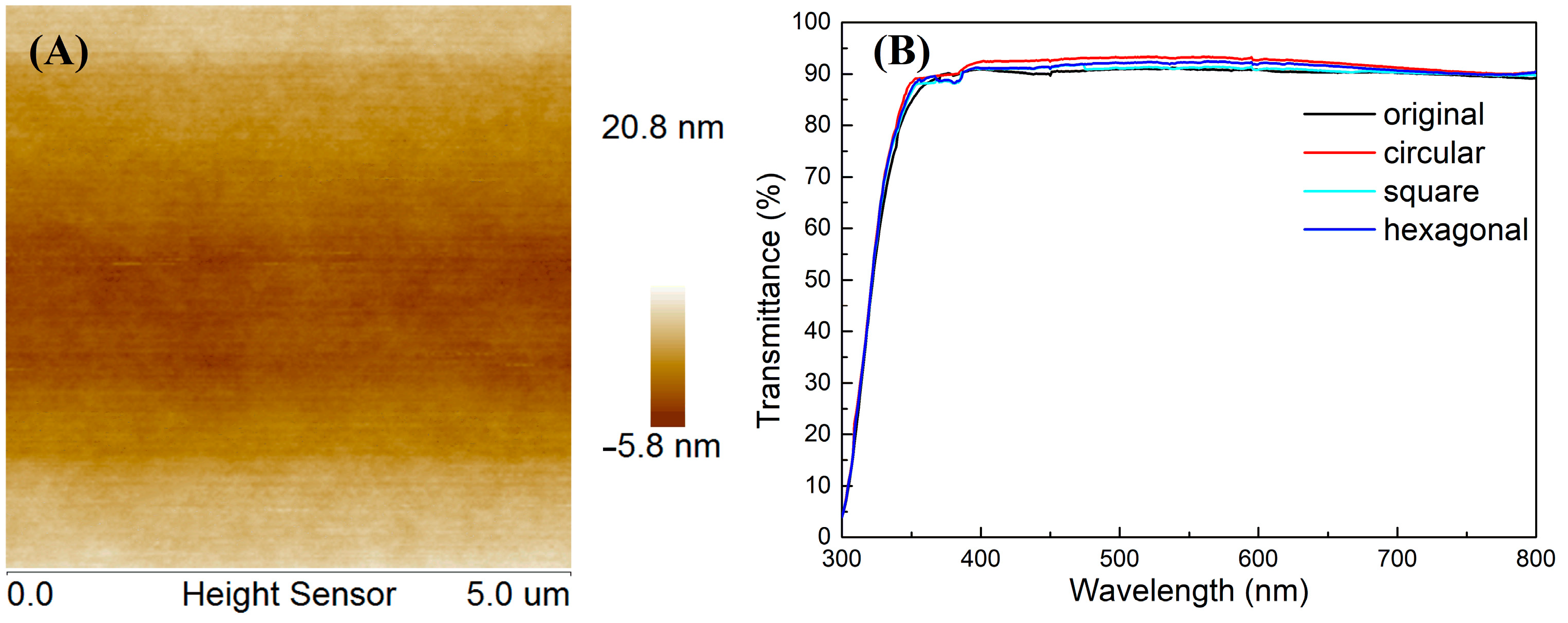
The optical properties of the organic–inorganic hybrid films were studied in this research work. AFM imaging of the organic–inorganic hybrid films detected an area range exceeding 5 μm × 5 μm size, as shown in
Figure 3A. It needs to be emphasized here that the film was prepared on a glass substrate surface at a spinning speed of 1800 rpm for 1 min and baked at 100 °C for 10 min. It can be clearly seen that the organic–inorganic hybrid films have a clean and flat surface. The light transmission properties of these films are shown in
Figure 3B.
Figure 3B shows that the organic–inorganic hybrid films have a relatively high light transmission—the transmittance value is almost over 90% in the visible light range of 350–800 nm, and the films show potential application value in the optical field. We can also see from
Figure 3B that the organic–inorganic hybrid films with MLAs have good light transmittance properties.
3.2. Surface Morphology and Outlines of the Hybrid Film MLAs
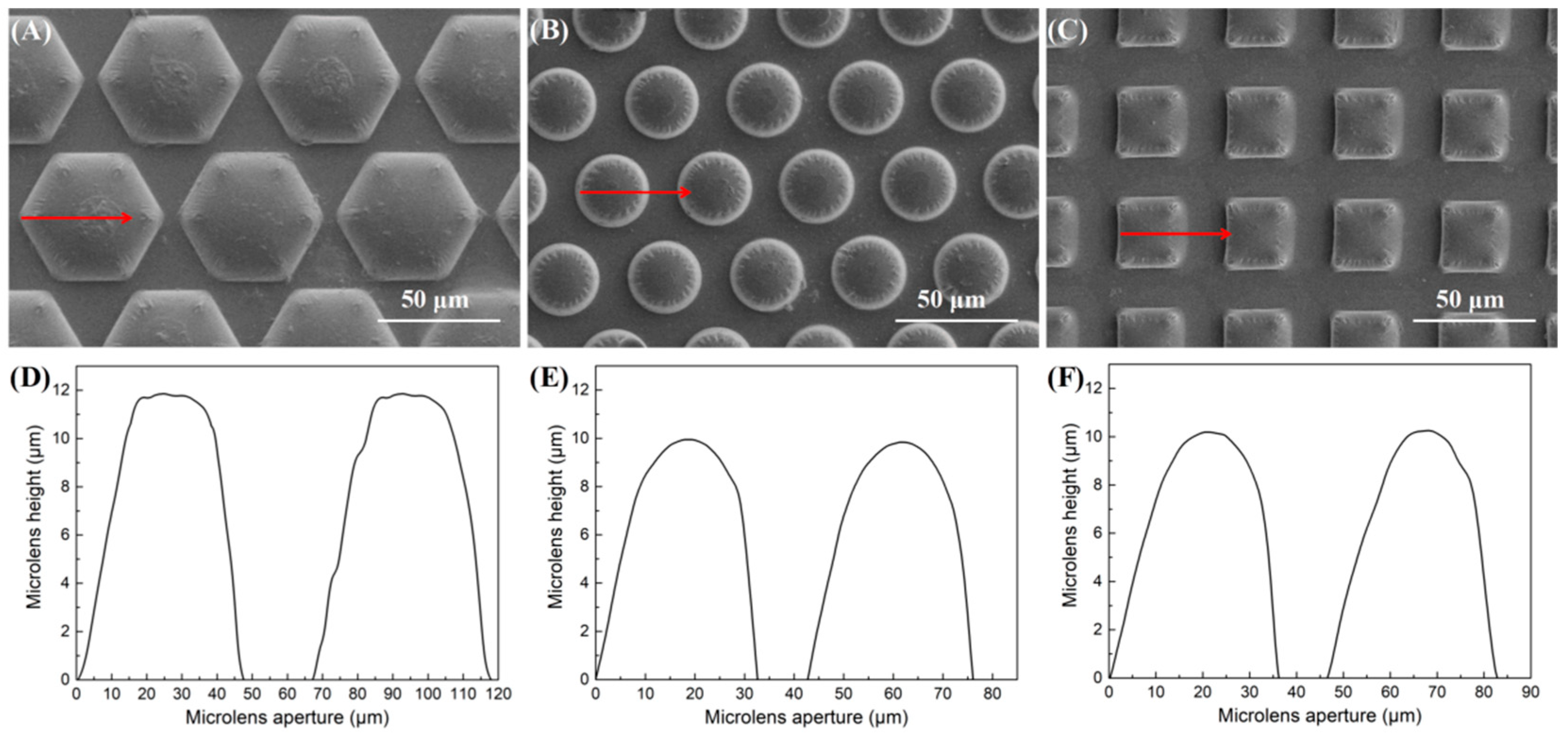
The SEM images and outlines of the hybrid film MLAs built on silicon solar cells are shown in
Figure 4. It can be seen from
Figure 4A–C that the hybrid film MLAs have a regular arrangement without obvious defects. Additionally, it can be obtained from
Figure 4D–F that the values of the diameter or the side length of the MLAs are 47.5, 34.5, and 37.5 µm for the hexagonal, circular, and square MLAs, respectively. At the same time, the height of the MLAs are 11.5, 10.1, and 10.2 µm, respectively. It is revealed that there is some difference in the values of the fabricated MLAs, compared to those of the MLAs mask, which is caused by the thermal reflow and imprint process.
3.3. Optical Imaging Capabilities
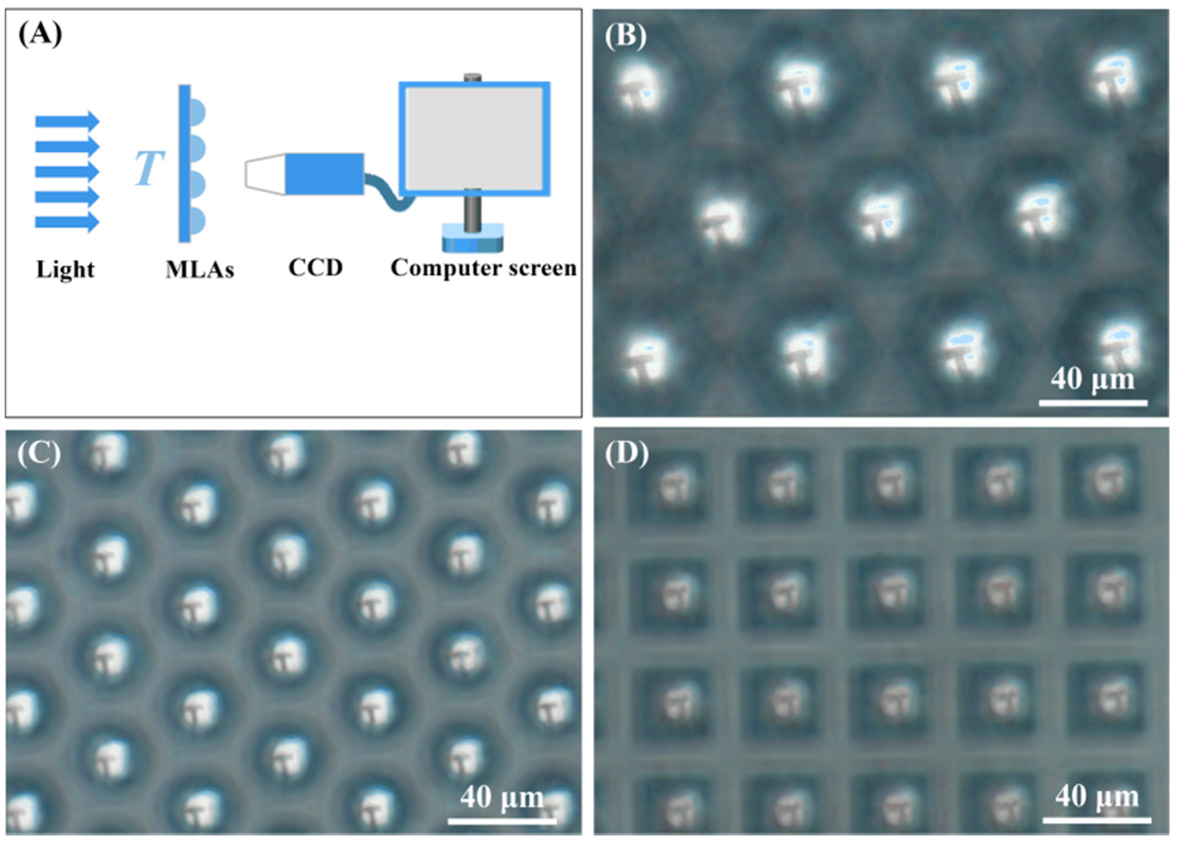
The optical imaging properties of the organic–inorganic hybrid film MLAs were observed by using an inverted optical microscope system. It needs to be emphasized here that the MLAs were fabricated on glass substrates and baked at 100 °C for 10 min. During the measurement, the glass sample with MLAs was placed in the center of the carrier plate and a small lntin-foil with the letter “T” was placed between the light source and the MLAs, as shown in
Figure 5A. By adjusting the relative position between the light source and the carrier plate, the focus situation changed, and the imaging result of the letter “T” in the system was obtained. It can be easily seen in
Figure 5B–D that the MLAs have good imaging performance, especially for the circular MLAs in
Figure 5C.
3.4. Contact Angle and Laser Diffraction
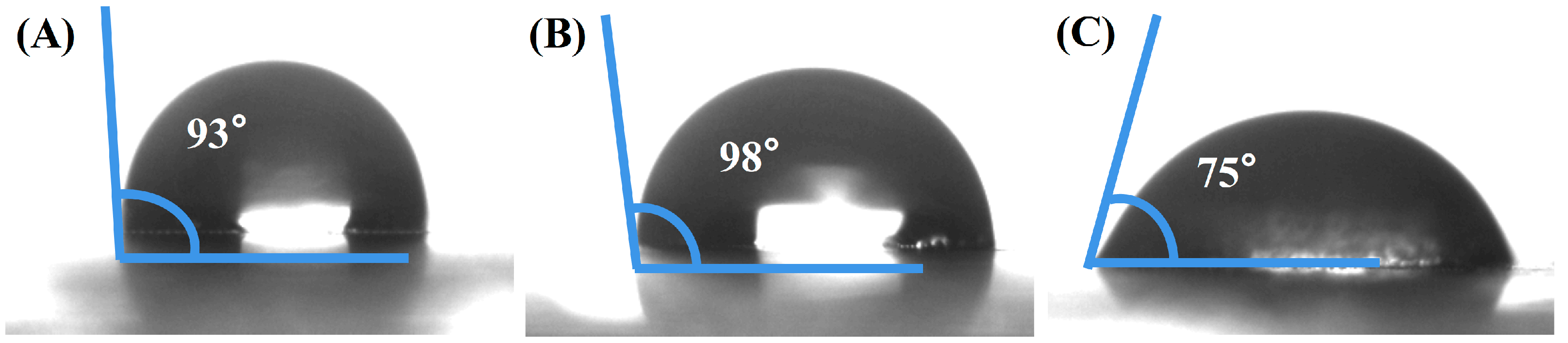
Figure 6 shows the contact angle measurement results of the hybrid film MLAs built on silicon solar cells. The contact angles are measured by dropping about 30 μL of water onto the surface of the cells. Water droplets on the surface of MLAs can be observed with an optical microscope and captured by a camera. It can be seen from
Figure 6 that the contact angles are 75°, 93°, and 98°, respectively, for the square, hexagonal, and circular MLAs, showing good hydrophobic properties. Solar cells with a microlens structure have good self-cleaning ability, thanks to the super hydrophobicity of the MLAs structure [
21].
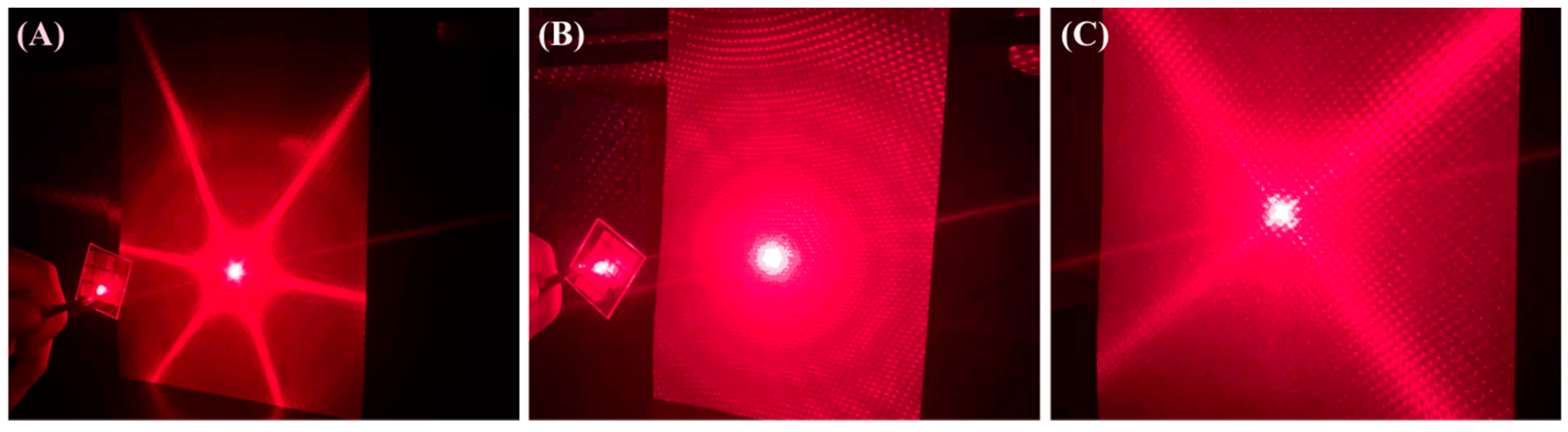
Figure 7 shows the laser diffraction properties of the organic–inorganic hybrid film MLAs prepared on clean glass substrate surfaces. The laser diffraction imaging system was constituted of an MLAs sample, a piece of clean A4 paper, and a laser pen. It should be emphasized that the diameter of the laser was about 2 mm. During the process, a red laser beam was passed through the hybrid film MLAs and irradiated onto the white paper; photographs were taken to visualize the scattered light. It can be seen in
Figure 7 that the beam of laser light is scattered when it passes through the organic–inorganic hybrid film MLAs, and a beautiful diffraction pattern is formed on the A4 paper. The most obvious effect is seen on the circular MLAs (in
Figure 7B). It should be mentioned that this scattering causes the propagation direction of the light to change, and a shift from normal incidence to incidence at a certain oblique angle, which can reduce the escape of light into air [
22].
3.5. Transmission Mechanism of Light on Silicon Solar Cells
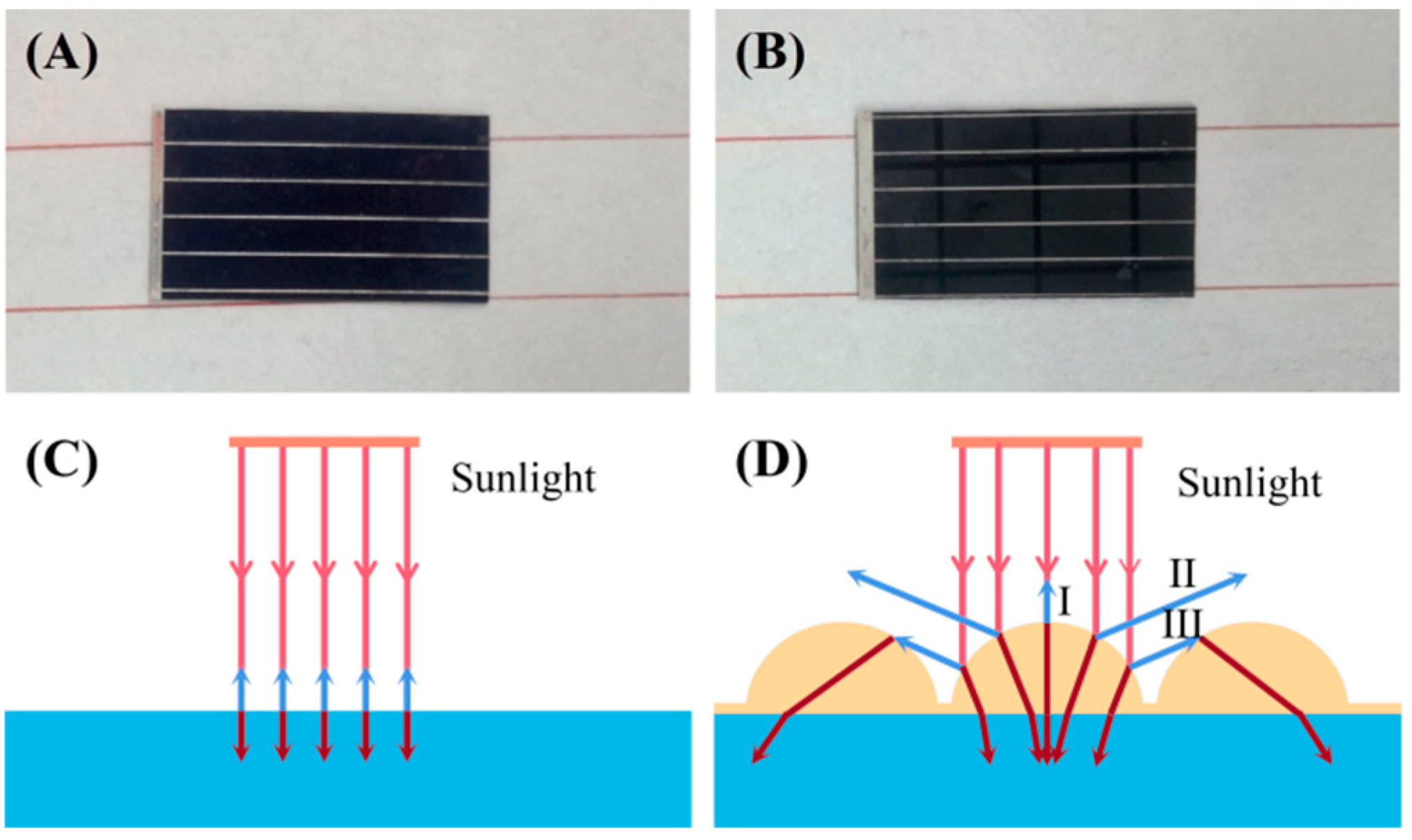
The as-prepared MLAs were built on silicon solar cells. The photographs of the silicon solar cells (A) without the MLAs and (B) with the MLAs are shown in
Figure 8A–B. The square areas in
Figure 8B are the MLAs. The size of the silicon solar cells is 2 cm × 1.5 cm.
Figure 8C–D shows the transmission mechanism of light on the silicon solar cell devices. When the light is incident vertically on the bare silicon solar cell devices, it reflects back to the original path, as shown in
Figure 8C. If the light hits the surface of a silicon solar cell with MLAs vertically, mainly three kinds of reflection paths (I, II, III) are noted, as shown in
Figure 8C. Lights I and II are completely dissipated in air, and light III can be absorbed again by the silicon solar cells to improve the utilization of light energy. The local heat received on the solar cell is different with varying types of MLAs. In addition, they can receive more heat when exposed to more sunlight.
3.6. Performance Characteristics
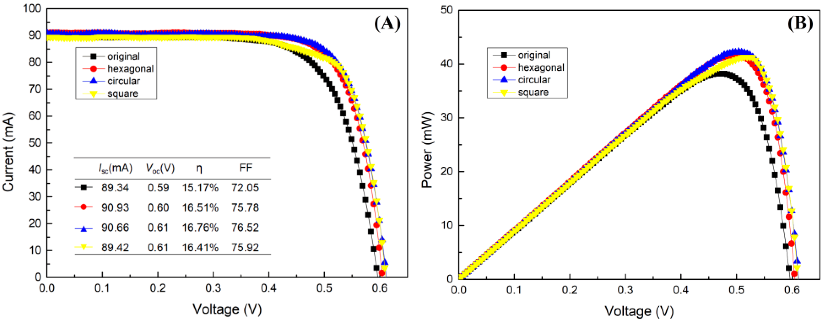
The photovoltaic performances, including current voltage and power of the silicon solar cells with hybrid film MLAs, were compared with a bare cell device (shown in
Figure 9). It can be seen from
Figure 9A that the open circuit voltages (V
oc) of the silicon solar cells have no significant difference. At the same time, the PCE of the silicon solar cell devices with hexagonal MLAs, circular MLAs, and square MLAs can be calculated as 16.51%, 16.76%, and 16.41%, respectively. Obviously, there is a maximum PCE improvement of about 10.48% for the silicon solar cell with circular MLAs. Finally, we can also see in
Figure 9B that the values of the maximum power (P
max) of the silicon solar cells with hexagonal MLAs, circular MLAs, and square MLAs are 41.62 mW, 42.25 mW, and 41.34 mW, respectively. It should be emphasized that the data obtained in the experiments have been rounded to two significant figures. From the above results, it can be clearly seen that the MLAs are able to improve the performance of silicon solar cells, especially circular MLAs.
4. Conclusions
In conclusion, three types of MLAs were fabricated on organic–inorganic hybrid films’ surface by using UV nanoimprint technology, and the MLAs were applied on silicon solar cells. The optical and surface morphology features of both the organic–inorganic hybrid films and the MLAs were characterized. The test results revealed that the organic–inorganic hybrid films have a smooth surface and a relatively high optical transmittance of above 90% in the visible light range. In addition, the MLAs have a flat and clear surface and relatively good optical imaging properties. Furthermore, the hydrophobic and laser diffraction properties of the MLAs were also studied. Finally, photovoltaic performances, including the current voltage and power of the silicon solar cells with hybrid film MLAs were investigated, showing a maximum PCE improvement by 10.48% for the silicon solar cell device with circular MLAs. The above results show that this is a simple and effective method to fabricate hybrid film MLAs on silicon solar cells, resulting in significant improvement in photoelectric conversion efficiencies.
Author Contributions
Writing—review and editing, X.Z.; writing—original draft preparation, Y.B.; data curation, S.L.; project administration, W.Z. and F.H. All authors have read and agreed to the published version of the manuscript.
Funding
National Natural Science Foundation of China (NSFC) (Nos: 61605086, 51602160, 61574080, 61274121).
Institutional Review Board Statement
Not applicable.
Informed Consent Statement
Not applicable.
Data Availability Statement
Not applicable.
Conflicts of Interest
The authors declare no conflict of interest.
References
- Hosseini, S.E.; Wahid, M.A. Hydrogen from solar energy, a clean energy carrier from a sustainable source of energy. Int. J. Energy Res. 2019, 44, 4110–4131. [Google Scholar] [CrossRef]
- Neumüller, A.; Sergeev, O.; Heise, S.J.; Bereznev, S.; Volobujeva, O.; Salas, J.F.L.; Vehse, M.; Agert, C. Improved amorphous silicon passivation layer for heterojunction solar cells with post-deposition plasma treatment. Nano Energy 2017, 43, 228–235. [Google Scholar] [CrossRef]
- Hara, K.; Jonai, S.; Masuda, A. Potential-induced degradation in photovoltaic modules based on n-type single crystalline Si solar cells. Sol. Energy Mater. Sol. Cells 2015, 140, 361–365. [Google Scholar] [CrossRef]
- Gai, B.; Sun, Y.; Chen, H.; Lee, M.L.; Yoon, J. 10-fold-stack multilayer-grown nanomembrane gaas solar cells. ACS Photon. 2018, 5, 2786–2790. [Google Scholar] [CrossRef]
- Yu, Y.; Zhang, F.; Yu, H. Self-healing perovskite solar cells. Sol. Energy 2020, 209, 408–414. [Google Scholar] [CrossRef]
- Zhang, D.; Rong, Y.; Hu, Y.; Mei, A.; Han, H. Hole-conductor-free perovskite solar cells. MRS Bull. 2020, 45, 449–457. [Google Scholar] [CrossRef]
- Wali, Q.; Iftikhar, F.J.; Khan, M.E.; Ullah, A.; Iqbal, Y.; Jose, R. Advances in stability of perovskite solar cells. Org. Electron. 2020, 78, 105590. [Google Scholar] [CrossRef]
- Brockett, T.J.; Rajagopalan, H.; Laghumavarapu, R.B.; Hufakker, D.; Rahmat-Samii, Y. Electromagnetic characterization of high absorption sub-wavelength optical nanostructure photovoltaics for solar energy harvesting. IEEE T. Antenn. Propag. 2013, 61, 1518–1527. [Google Scholar] [CrossRef]
- Hsu, C.-H.; Zhang, X.-Y.; Zhao, M.J.; Lin, H.-J.; Zhu, W.-Z.; Lien, S.-Y. Silicon heterojunction solar cells with p-type silicon carbon window layer. Crystals 2019, 9, 402. [Google Scholar] [CrossRef] [Green Version]
- Wang, Z.; Sun, C.; Wang, X. Modification of front surface antireflection of silicon solar cells with composite metallic nanoparticle arrays. Plasmon. 2016, 12, 589–596. [Google Scholar] [CrossRef]
- Zhang, S.; Liu, M.; Liu, W.; Li, Z.; Liu, Y.; Wang, X.; Yang, F. High-efficiency photon capturing in ultrathin silicon solar cells with double-sided skewed nanopyramid arrays. J. Opt. 2017, 19, 105901. [Google Scholar] [CrossRef]
- Jiang, Y.; Shen, H.; Pu, T.; Zheng, C.; Tang, Q.; Gao, K.; Wu, J.; Rui, C.; Li, Y.; Liu, Y. High efficiency multi-crystalline silicon solar cell with inverted pyramid nanostructure. Sol. Energy 2017, 142, 91–96. [Google Scholar] [CrossRef]
- Huang, F.; Zhang, L.; Li, S.; Fu, J.; Zhang, K.H.L.; Cheng, Q. Direct growth of graphene nanowalls on inverted pyramid silicon for schottky junction solar cells. ACS Appl. Energy Mater. 2021, 4, 6574–6584. [Google Scholar] [CrossRef]
- Huang, B.-R.; Yang, Y.-K.; Lin, T.-C.; Yang, W.-L. A simple and low-cost technique for silicon nanowire arrays based solar cells. Sol. Energy Mater. Sol. Cells 2012, 98, 357–362. [Google Scholar] [CrossRef]
- Wu, L.; Zhang, H.; Qin, F.; Bai, X.; Ji, Z.; Huang, D. Performance enhancement of pc-Si solar cells through combination of anti-reflection and light-trapping: Functions of AAO nano-grating. Opt. Commun. 2017, 385, 205–212. [Google Scholar] [CrossRef]
- Leem, J.W.; Guan, X.Y.; Choi, M.; Yu, J.S. Broadband and omnidirectional highly-transparent cover glasses coated with biomimetic moth-eye nanopatterned polymer films for solar photovoltaic system applications. Sol. Energy Mater. Sol. Cells 2015, 134, 45–53. [Google Scholar] [CrossRef]
- Lin, J.; Chen, M.; Ke, Y.; Ren, C.; Xu, Z.; Zhang, Y.; Fang, C. A compact and high-power silicon-wafer solar strip-cells-array module integrated with an array concentrator. Chin. Phys. B 2018, 27, 18802. [Google Scholar] [CrossRef]
- Ha, S.-H.; Yu, H.-W.; Jang, N.-S.; Kim, J.H.; Kim, S.-H.; Kim, J.-M. Compact and high-power dye-sensitized solar system integrated with low-cost solar-concentrating polymer lens. Sol. Energy Mater. Sol. Cells 2016, 155, 362–367. [Google Scholar] [CrossRef]
- Tseng, J.; Chen, Y.; Pan, C.; Wu, T.; Chung, M. Application of optical film with micro-lens array on a solar concentrator. Sol. Energy 2011, 85, 2167–2178. [Google Scholar] [CrossRef]
- Li, Y.; Jiang, T.; He, X.; Zhang, Y.; Fang, C.; Li, Z.; Lin, J.; Zhuang, Y. Cylindrical lens array concentrator with a nanonipple-array antireflective surface for improving the performances of solar cells. Opt. Commun. 2019, 439, 118–124. [Google Scholar] [CrossRef]
- Li, Y.; Zhang, Y.; Lin, J.; Fang, C.; Ke, Y.; Tao, H.; Wang, W.; Zhao, X.; Li, Z.; Lin, Z. Multiscale array antireflective coatings for improving efficiencies of solar cells. Appl. Surf. Sci. 2018, 462, 105–111. [Google Scholar] [CrossRef]
- Liu, D.; Wang, Q. Light-trapping surface coating with concave arrays for efficiency enhancement in amorphous silicon thin-film solar cells. Opt. Commun. 2018, 420, 84–89. [Google Scholar] [CrossRef]
Figure 1.
Design of MLAs masks with different arrangement shapes: (A) hexagonal combination arrangement, (B) circular combination arrangement, and (C) square combination arrangement.
Figure 1.
Design of MLAs masks with different arrangement shapes: (A) hexagonal combination arrangement, (B) circular combination arrangement, and (C) square combination arrangement.
Figure 2.
Experimental flowchart of MLAs built in bare silicon solar cells. (A) Spin-coating of photoresist thin films on a silicon substrate; (B) the photoresist films are placed under the irradiation of ultraviolet light with a mask; (C) thermal reflow process; (D) photoresist MLAs template; (E) slowly dumping the PDMS precursor over the MLAs template; (F) gently removing the PDMS to obtain the MLAs soft mold; (G) the PDMS mold is tightly attached to the hybrid films’ surface deposited on silicon solar cells; (H) exposing the sample to UV light for solidification; and (I) silicon solar cells are obtained with organic–inorganic hybrid film MLAs.
Figure 3.
(A) AFM image of the organic–inorganic hybrid film baked at 100 °C for 10 min, and (B) light transmission properties of the organic–inorganic hybrid film MLAs.
Figure 3.
(A) AFM image of the organic–inorganic hybrid film baked at 100 °C for 10 min, and (B) light transmission properties of the organic–inorganic hybrid film MLAs.
Figure 4.
The SEM images and corresponding outlines of the (A,D) hexagonal MLAs, (B,E) circular MLA and (C,F) square MLA built on the silicon solar cells’ surface; the length of the red arrows in the SEM images is 45.5 µm.
Figure 4.
The SEM images and corresponding outlines of the (A,D) hexagonal MLAs, (B,E) circular MLA and (C,F) square MLA built on the silicon solar cells’ surface; the length of the red arrows in the SEM images is 45.5 µm.
Figure 5.
Diagram of the imaging system (A), and inverted images of a small lntin-foil with letter “T” imaged by the hybrid film MLAs, (B) hexagonal MLAs, (C) circular MLAs, and (D) square MLAs.
Figure 5.
Diagram of the imaging system (A), and inverted images of a small lntin-foil with letter “T” imaged by the hybrid film MLAs, (B) hexagonal MLAs, (C) circular MLAs, and (D) square MLAs.
Figure 6.
The contact angles of water on the (A) hexagonal MLAs, (B) circular MLAs, and (C) square MLAs.
Figure 6.
The contact angles of water on the (A) hexagonal MLAs, (B) circular MLAs, and (C) square MLAs.
Figure 7.
Diffraction patterns of a laser beam passing through the hybrid film MLAs, (A) hexagonal MLAs, (B) circular MLAs, and (C) square MLAs.
Figure 7.
Diffraction patterns of a laser beam passing through the hybrid film MLAs, (A) hexagonal MLAs, (B) circular MLAs, and (C) square MLAs.
Figure 8.
Photographs of silicon solar cells (A) without MLAs and (B) with MLAs and the transmission mechanism of light on (C) a bare silicon solar cell device and (D) a silicon solar cell device with hybrid film MLAs.
Figure 8.
Photographs of silicon solar cells (A) without MLAs and (B) with MLAs and the transmission mechanism of light on (C) a bare silicon solar cell device and (D) a silicon solar cell device with hybrid film MLAs.
Figure 9.
(A) I-V curves and (B) P-V curves of silicon solar cells with square MLAs, circular hexagonal MLAs, and a circular MLAs structure, compared to those of a bare cell.
Figure 9.
(A) I-V curves and (B) P-V curves of silicon solar cells with square MLAs, circular hexagonal MLAs, and a circular MLAs structure, compared to those of a bare cell.
Table 1.
Specific values for the MLAs.
Table 1.
Specific values for the MLAs.
| MLAs Shape | Diameter/Side Length (μm) | Height (μm) | Space (μm) |
|---|
| Hexagonal | 30 | 10 | 5 |
| Circular | 30 | 10 | 12 |
| Square | 30 | 10 | 15 |
| Publisher’s Note: MDPI stays neutral with regard to jurisdictional claims in published maps and institutional affiliations. |
© 2022 by the authors. Licensee MDPI, Basel, Switzerland. This article is an open access article distributed under the terms and conditions of the Creative Commons Attribution (CC BY) license (https://creativecommons.org/licenses/by/4.0/).


