Article

Electronic Structure of Graphene on the Hexagonal Boron Nitride Surface: A Density Functional Theory Study

by
Gladys Casiano-Jiménez
1,2,
César Ortega-López
1,2,
Jairo Arbey Rodríguez-Martínez
3,
María Guadalupe Moreno-Armenta
4 and
Miguel J. Espitia-Rico
5,*
1
Grupo Avanzado de Materiales y Sistemas Complejos GAMASCO, Universidad de Córdoba, Montería 230001, Colombia
2
Doctorado en Ciencias Física, Universidad de Córdoba, Montería 230001, Colombia
3
Grupo de Estudio de Materiales GEMA, Universidad Nacional de Colombia, Bogotá 111321, Colombia
4
Centro de Nanociencias y Nanotecnología, Universidad Nacional Autónoma de México, Km 107 Carretera Tijuana-Ensenada, Apdo Postal 14, Ensenada 22800, Mexico
5
Grupo GEFEM, Universidad Distrital Francisco José de Caldas, Bogotá 110231, Colombia
*
Author to whom correspondence should be addressed.
Coatings 2022, 12(2), 237; https://doi.org/10.3390/coatings12020237
Submission received: 14 October 2021 / Revised: 27 November 2021 / Accepted: 8 December 2021 / Published: 12 February 2022
(This article belongs to the Special Issue Application of Graphene and Two-Dimensional Materials in Thin Films)

Abstract

:
Poor electron-related cutting current in graphene-based field-effect transistors (FETs) can be solved by placing a graphene layer over a hexagonal boron nitride (BN) substrate, as established by Giovannetti et al. and other researchers. In order to produce high-quality results, this investigation uses 2 × 2 cells (~2.27% mismatch), given that larger cells lead to more favourable considerations regarding interactions on cell edges. In this case, the substrate-induced band gap is close to 138 meV. In addition, we propose a new material based on graphene on BN in order to take advantage of the wonderful physical properties of both graphene and BN. In this new material, graphene is rotated with respect to BN, and it exhibits a better mismatch, only ~1.34%, than the 1 × 1-graphene/1 × 1-BN; furthermore, it has a very small bandgap, which is almost zero. Therefore, in the bands, there are electronic states in cone form that are like the Dirac cones, which maintain the same characteristics as isolated graphene. In the first case (2 × 2-graphene/2 × 2-BN), for example, the resulting band gap of 138 meV is greater than Giovannetti’s value by a factor of ~2.6. The 2 × 2-graphene/2 × 2-BN cell is better than the 1 × 1-graphene/BN one because a greater bandgap is an improvement in the cutting current of graphene-based FETs, since the barrier created by the bandgap is larger. The calculations in this investigation are performed within the density functional theory (DFT) theory framework, by using 2 × 2-graphene/2 × 2-BN and 13 × 13 -graphene/ 2 3 × 2 3 -(0001) BN cells. Pseudopotentials and the generalized gradient approximation (GGA), combined with the Perdew–Burke–Ernzerhof parametrization, were used. Relaxation is allowed for all atoms, except for the last layer of the BN substrate, which serves as a reference for all movements and simulates the bulk BN.

1. Introduction

Materials such as graphene and boron nitride (BN) are highly valued in cutting-edge nanotechnologies. Graphene has exceptional physical properties: it is lightweight and has high electrical and thermal conductivity, high electronic mobility, and zero bandgaps [1,2,3,4,5,6,7,8,9,10,11,12,13,14]. BN and other BN-based compounds are promising materials that are widely used in devices operating at high temperatures, high radio frequencies, and high-power laser diodes, or in devices required to operate in the ultraviolet region, solar detectors, field-effect transistors, and high-mobility transistors [15,16,17,18,19,20,21,22,23].
However, when BN and graphene are working in isolation or independently from one another, their applications are restricted, since they are inert within chemical interactions, which hinders chemical bonds, which are necessary for devices. For instance, a junction with a substrate is necessary to form a field-effect transistor (FET). Graphene and BN can work as a single collective material, making them highly useful in nanotechnologies.
Recent breakthroughs in material growth techniques have enabled stable combinations of graphene and BN. A relevant example is a union between 1 × 1-graphene and 1 × 1-BN, which has been thoroughly studied [24,25,26,27,28] despite the difficulty of obtaining it. The quality of the combinations can be affected by many factors, and the Dirac cones can disappear or become damaged. These cones are significant in nanoelectronic devices, because they guarantee the high mobility of the charge carriers. One of the main problems seen in the junctions is the mismatch between the crystal lattices. A 2D 1 × 1 hexagonal boron nitride (1 × 1-BN) has a lattice mismatch with 1 × 1 graphene in the range of 1.6% to 2.2%, depending on the lattice constant defined for each material. h-BN/graphene junctions in 2 × 2 cells exhibit a similar mismatch, although 2 × 2 cells offer better results in calculations. The present investigation uses 2 × 2 cells, given that the software used to calculate DFT-based mechanical-quantum properties smoothens the effect over the edges when a cyclic crystal lattice is chosen. This can be evidenced by comparing the band gaps of the BN/graphene junction obtained by Giovannetti et al. [29] (53 meV) and those of this investigation (138 meV).
According to Giovannetti et al. and other researchers, the appearance of a gap causes the Dirac electrons to have a finite mass, which would facilitate the use of graphene in electronic devices. In the case of field-effect transistors (FETs), Giovanetti et al. propose a structure of graphene over BN that opens a gap between the Dirac cones [29]. In the present investigation, we propose an interface with a different gap than for 1 × 1 graphene/1 × 1 BN. The calculations were performed within the framework of density functional theory.

2. Structures and Methods

Quantum ESPRESSO (QE) [30] code and pseudopotential [31,32] approximations were used to perform all calculations in this investigation. Exchange and correlation effects are included by using the GGA approximation combined with the Perdew–Burke–Ernzerhof parametrization [33].
Additionally, Van der Waals interactions are considered through the DFT-D2 approximation [34], within the density functional theory framework [35,36]. For the substrate simulation, a seven-monolayer slab of (0001) h-BN in space group #194 was built with planar hexagonal geometry and perpendicular to the z-axis. The z-axis is perpendicular to the only graphene layer over the BN. The slabs are separated by a 12 Å vacuum to avoid interactions between the images of adjacent slabs.
In Table 1, the main input parameters for lattice A and lattice B, such as the lattice constants of the graphene and BN surface, the B-N (lB-N) and C-C (lC-C) bond lengths are listed. In addition, some of the initial calculation parameters, such as the shear energies for plane-wave expansion, the charge density expansion, and the numbers K point obtained with the Monkhorst–Pack method [37], are shown. The lattice constants for BN and graphene in isolation and the graphene/BN structures are calculated from a minimization process of plots of energy vs. volume for BN and energy vs. lattice constant for graphene; the details are not included in this paper. In all the calculations, the convergence of the self-consistent cycles and the total energy and the stability of their value with different parameters, such as cut-off of plane waves and cut-off of charge density, were closely monitored. All the calculations were performed using a vc-relax calculation mode in which all atoms in the supercell move in the three directions, and the smearing technique proposed by Methfessel–Paxton [38] was used.
This investigation considers two structures of graphene/BN: a 2 × 2-graphene/2 × 2-(0001) BN cell with seven monolayers (or simply 2 × 2-graphene/2 × 2-BN), and a 13 × 13 -graphene/ 2 3 × 2 3 -(0001)-BN, with seven slabs. For simplification purposes, the 2 × 2-graphene/2 × 2-BN is labelled A-lattice and the 13 × 13 -graphene/ 2 3 × 2 3 -(0001)-BN is labelled B-lattice. Their respective mismatches were ~2.27% and ~1.34%. The mismatch can be understood as the relative deviation of the graphene lattice constant with respect to that of the BN lattice constant in the graphene/BN structure. For an arbitrary configuration i j × i j grephene / k l × k l BN , the mismatch is given by Equation (1)
mismatch = ( k l ) a BN ( i j ) a graphene ( k l ) a BN × 100 %
where a BN and a graphene are the values of the lattice constants of BN and graphene, respectively. These values are shown both in the 1 × 1 configuration and in Table 1.
The convergence criteria defined for energy and force calculations were 10−4 Ry and 10−3 Ry/Bohr, respectively.
This convergence criterion is widely accepted in the scientific community and by users of the pseudopotential method, and it is recommended in the QE code. In addition, the charge density cut-off is within the optimal range for QE. This optimal range is between four and eight times the cut-off of the expansion of the plane waves (PW). This investigation works with a factor of 10 times the cut-off of the expansion of PW in order to diminish some small oscillations in the total energy. Since the energy convergence is 10−4 Ry ~1.4 meV, then, based on all the above-mentioned considerations, that value can be established (+/−1 meV o +/−2 meV) as the limit value for considering it to be a trustworthy value for the energy.
When a new material is proposed and calculations are carried out using DFT, the question of the accuracy and precision of the theory and the calculations reappears. How accurate are the calculations of the lattice constants, the bond lengths, and the unit cell volume? These amounts are determined with accuracy in the range of 4~10%. But precision in elastic properties is about 30%. The worst scenario is for electronic properties and formation energies, where, for example, the error can be up to 100% in some cases. In these cases, the accuracy of the calculations is very poor, because they result in values that are far from those of the experimental measurements. The error in the bandgap can be some units of eV. Through the hybrid XC-functionals and GW approach, the errors decrease to a few tenths of an eV. In the case of graphene, the majority of the calculations performed with DFT using GGA produce the zero-band gap precisely, making them highly accurate (achieving the same experimental value), and their accuracy is also confirmed because they are reproducible. In the case of structures A and B, the results for the bandgap are 138 meV and 2 meV, respectively. Therefore, and based on what is known about the DFT band gap problem, we can affirm that our results give a maximum for the bandgap. Still, expanding the range of indeterminacy of the bandgap from 1.4 meV to +/−2 meV in structure B, approximated by an analysis of the value of convergence in the calculations, we could say that the minimum value of the bandgap for structure B would be in the range of energies between 0 and 4 meV. Therefore, our gap value cannot be guaranteed. A bandgap of 2 meV must be taken as the lower limit for the value of the bandgap. The real value will only be known when an experimental measurement is done.
The A-lattice and B-lattice were chosen by the following procedure: We constructed a computer program that calculates the mismatch between the two lattices (BN and graphene), considering rotations of one lattice with respect to the other, leaving one lattice fixed, and vice versa. Another, simpler way of calculating new lattices is by multiplying the lattice constants of BN or graphene by natural or irrational numbers such as 3 , 7 , 13 , or multiplying by 2 3 or 3 7 , i.e., multiplying by integer multiples of the irrational ones. After that, the code calculates the mismatch for each combination and chooses those combinations that produce a lattice with a mismatch of a lower percentage, such as 2% or 3%. The lattices found by the program are candidates for new materials. After determining a candidate, other additional configurations can still be obtained for the same crystal lattice combination. This is carried out by displacing one lattice with respect to the other until obtaining symmetrical and favourable configurations from the chemical point of view. That is, the graphene can be displaced until a C atom is on the centre of the BN hexagon or C is located on top of the B atom or the B-N bridge. Lattice-A and lattice-B were optimized for energy vs. lattice constant and energy vs. separation between graphene and BN. The configurations with the lowest total energy are preferred (see next section, Figure 3, as an example). With that process, the B-lattice was born, see next paragraph Figure 2, and therefore, in this investigation, a new material is proposed with special characteristics that enable designing new devices based on graphene. Up to the publication date of this investigation, no one has proposed the B-lattice.
Figure 1 and Figure 2 correspond to the A- and B-lattice configurations. Figure 1a includes a top view of A-lattice, where each C atom is located precisely on top of each B atom. All C and B atoms have hexagonal symmetry. Figure 1b shows a section of the slab, revealing that the graphene sheet is located over the slab. BN layers constitute the surface of the substrate. Figure 2 shows a top view of the B-lattice, including some positions such as (1) C atom on B atom; (2) B forming a bridge between adjacent C atoms; (3) B in bridge position between nonadjacent C atoms; (4) B atom at the centre of the graphene hexagon; and (5) B atom in the centre of the cell, right at the intersection of the green lines.

3. Results

All discussions and conclusions are based on the results of total energy calculations performed using DFT. The first part of this section focuses on the structural properties. The main objective is to show that the aforementioned structures A and B are possible through energy-related considerations. The second section dwells on electronic properties. The main objective of this section is to prove that Dirac’s cones are maintained with a very small gap. The gap value is close to the convergence parameter, while the bandgap is likely to close to zero.

3.1. Structural Parameters

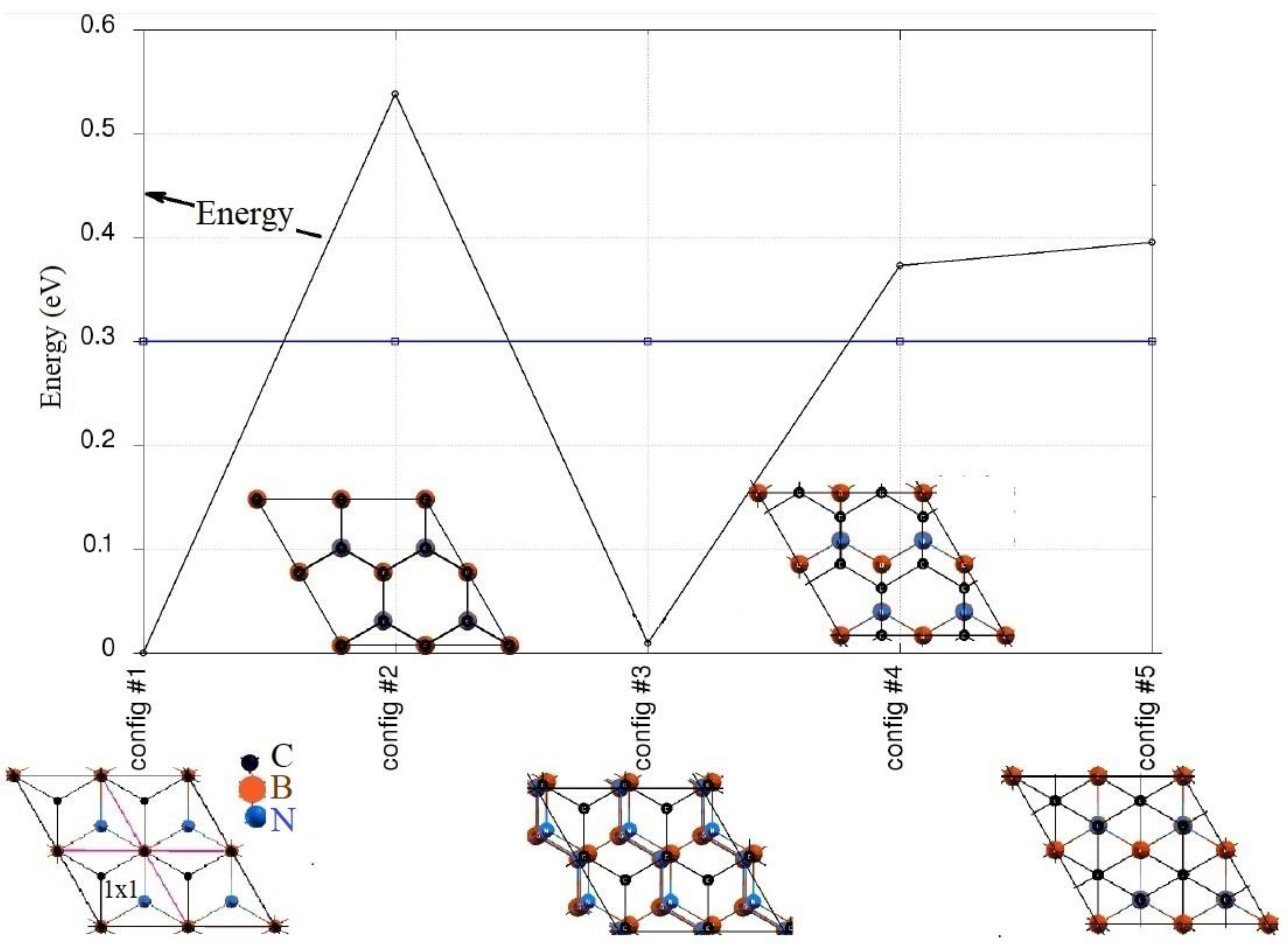
3.1.1. Structural Properties of the A-Lattice

In the A-lattice structure, there are five sub-configurations, obtained by initially having a C atom remain over a B (or N) atom, bridged between adjacent or non-adjacent atoms or forcing it to remain at the centre of a hexagon. Afterwards, complete relaxation of the crystal is performed. Different configurations for a single structure offer new possibilities in terms of band structure and reducing the total energy, hence giving more stability. Figure 3 shows the total energy as a function of the configuration. The minimum energy level serves as a reference.
It can be concluded that sub-configuration #1 has a minimum energy level, followed very closely by sub-configuration #3. Sub-configuration #1 has a classic pattern and is well-known for its 1 × 1 and β 2 × 2 cells. In this case, C and B are on top of each other. Giovannetti et al. [1] show similar results.
Once the relaxation process is finished, the lattice constants and bond lengths tend to vary. In the case of graphene, the new lattice constant is 2.4785 Å and the new C-C bond length is 1.4310 Å. This corresponds to a 1.4% increase in the lattice constant compared to the values obtained with isolated graphene. Figure 4 shows a relaxed cell, along with its bond length and lattice constant. Afterwards, the graphene expands and preserves its hexagonal structure. In the case of BN, the separation between layers is 3.0962 Å, the lattice constant is 2.5100 Å, and the bond length is 1.4492 Å. After the relaxation process, the separation between layers of BN remains within the [2.9080 Å; 2.921 Å] range, the lattice constant is 2.4783 Å, and the B-N bond length is 1.4332 Å. It can be seen that the separation between layers is reduced by 5.8% (compared to the central value of the variation range), and the lattice constant is diminished by up to 1.3% and the bond length by 1.6%. Hence all parameters are reduced for BN. Furthermore, Figure 2 shows that the first and second layers are contracted by ~6.4%. The contraction between the second and third layers is close to 6.3%, while the contraction between the third and fourth layers is 5.7%.
Seeking to analyse the thermodynamic stability in the A-lattice and B-lattice, we determined the formation energy.
The formation energy E f is calculated according to Equation (2) [39,40]
E f = 1 A ( E graphene / BN E BN iso E graphene iso )
where E graphene / BN is the total energy of the graphene/BN interface, E BN iso and E graphene iso are the total energies of the isolated BN slab and the graphene slab, respectively, and A is the interface area.
The values obtained for the formation energy E f of structures A and B are shown in Table 2.
.
From the results shown in Table 2, it can be inferred that negative formation energies indicate that these structures are thermodynamically stable, suggesting that the structures could be synthesized in experiments. Finally, We did not find in the literature formation energy values for the graphene/(0001)BN-surface structure with the same configurations considered in this investigation.

3.1.2. Structural Properties of the B-Lattice

The B-lattice is a 13 × 13 grafeno/ 2 3 × 2 3 (0001)-BN structure with 52 C atoms, 84 N atoms, and 84 B atoms (see Figure 2). Different configurations were calculated, with B-lattice being the most stable configuration, shown in Figure 2. Additionally, this figure displays two 1 × 1 cells as a visual guide in order to facilitate seeing its structure and its orientation. The rotation between BN unitary cells and graphene is illustrated, where the grey section represents the 1 × 1 BN cell and the pink section represents graphene. The angle between the cells is ~46.9°.
The resulting mismatch is 1.34%. After relaxation, the lattice constant for graphene decreases by 0.43% and the hexagonal structure is approximately maintained. The lattice constant of BN decreases by 0.7%. The two layers of BN at the top of the cell move closer to each other by 4.0%. The second and third layers move closer to each other by 3.8% and the next two layers by 3.7%. Lastly, the separation between the graphene layer and the first BN layer increases by 0.6%.

3.2. Electronic Properties

The electronic properties were calculated for both structures. Figure 5 and Figure 6 show the bands for A-lattice and B-lattice. Figure 5a includes all the bands between ~−20 eV and ~10 eV in the ΓΚΜΓ range, which marks the boundary of the irreducible part of the first Brillouin zone (FBZ) in the hexagonal lattice. The zero-energy level is defined as the Fermi level. By contrast, Figure 5b and Figure 6b display the bands within the small range between −1 eV and 1 eV and the vicinity of high symmetry point Κ of the FBZ. The arrows indicate the spin polarization, given that the calculations were carried out with polarized spin. However, the bands for both spin directions are identical. The bands can be seen as planes with almost no dispersion. Figure 5a and Figure 6a show a similar representation of the Dirac cones, which is not located at point Γ, which is the most symmetrical point of the FBZ in hexagonal lattices. This occurs in semi-metallic pristine graphene. The valence band (VB) and the conduction band (CB) seem to be touching at the high-symmetry point K. Figure 5b corresponds to a zoomed view of the region, confirming that the bands do not touch. There is a gap of 138 meV for A-lattice and 2 meV for B-lattice (which are underestimated by DFT).
Additionally, several theoretical investigations have indicated that the bandgap could depend on the stacking alignment and the applied electric field, with values ranging from 0 to 130 meV [41,42,43,44,45,46,47,48,49,50,51,52,53,54]. The 138 meV band gap value calculated for the A-lattice is slightly higher than the values predicted in the range but is greater than the values reported by by Giovannetti et al. [1] of 53 meV, Behara et al. [55] of 59 meV, and Lui et al. [56] of 120 eV. However, it is slightly less than the value reported by Kharche et al. [57] of 145 eV, calculated using GW corrections, and it is much less than the value of 325 meV, calculated by Sevilla et al. [58], using the B97 corrected by vdW. D functional.
Experimental studies have been reported that confirm the appearance of a bandgap in graphene grown on hBN, whose values are between 15 and 40 meV [59,60,61,62]. These values are obtained via transport measurements and the magneto-optical spectroscopy technique.
In summary, the bandgap of 138 meV calculated for the new proposed 2 × 2-graphene/2 × 2-(0001) BN structure is an improvement in the cutting current of graphene-based FETs because the barrier associated with the bandgap is relatively large. Additionally, the A- and B-lattice structures are classified as direct semiconductors with a narrow-forbidden gap. In the vicinity of zero energy, the outlined bands seem to be Dirac’s cones at point K. Their shape is similar to a cone, yet they have a parabolic nature with a very large second derivative, producing carriers with very small effective mass. An appropriate name would be pseudo-Dirac cones (PDCs). Calculations show that the composition of such PDCs is mainly pz orbitals of C and B for both lattice structures. One section of these orbitals connects the graphene layer with the first upper layer of BN, while others form π planar orbitals in the graphene. Additionally, the mobility of the carriers must be high, given that this is an identifiable property of real Dirac cones, even if they are displaced from the centre of the FBZ. Nonetheless, the masses of carriers are finite in this case. The bands in Figure 5 seem to come from a simple composition, as seen when the bands are overlapped and drawn on transparent paper. The overlapping bands are the surface bands (0001) of BN and graphene. This effect is only achieved because the interaction between layers is very small, only creating energy shifts. This partially explains the appearance of pseudo-cones.
Improving the poor presence of electrons in the cutting current of graphene-based FETs (field-effect transistors) requires the definition of a forbidden gap, as shown in Figure 5b and Figure 6b. Structure B is not recommended for use in FETs, because its gap is almost zero. The slight mismatch (~1.34%) of B-lattice makes it a better option for coupling than A-lattice. As a consequence, the energy gap becomes narrower, allowing the carriers in B-lattice to have increased mobility while maintaining very small effective masses.

4. Conclusions

DFT calculations were carried out regarding the graphene/BN interface, seeking to propose new structures that can improve some electronic or optoelectronic devices, such as FET’s based on graphene. This investigation proposes a new, highly symmetric interface: 13 × 13 -graphene layer over a   2 3 × 2 3 -(0001) BN layer (labelled as B-lattice), which has a quasi-zero bandgap, according to our calculations, and exhibits Dirac pseudo-cones. Our calculations for the 2 × 2-graphene/2 × 2-BN supercell show a bandgap of 138 meV. Therefore, this supercell can be used to improve the electronic performance of FETs, supporting the idea of Giovannetti et al. [29] and other researchers.
The negative formation energies indicate that these structures (A and B) are thermodynamically stable, suggesting that the structures could be synthesized in experiments.
Overall, the bands of A-lattice and B-lattice structures exhibit differences in terms of density of state, given that B-lattice has more atoms than A-lattice, which implies more mechanical-quantum states and carriers. In addition, in this investigation a new way to join materials is proposed: it consists of calculating the lattice constant for different cells of two materials, not necessarily units, and fitting different values until the mismatch of the cells decreases, as is explained in the section structures and methods. This new structure B with an almost zero gap and possible Dirac cones could serve as a contact with other materials, because BN can serve as a buffer layer. This contact, analogous to graphene, has good electrical and thermal conductivity.

Author Contributions

G.C.-J., J.A.R.-M. and M.G.M.-A. performed computational calculations, M.J.E.-R., C.O.-L. and J.A.R.-M. carry out the analysis of the data obtained, writing the manuscript and validation. All authors have read and agreed to the published version of the manuscript.

Funding

This research was funded by Universidad de Córdoba located in Montería Colombia, project number FCB-07-19.

Institutional Review Board Statement

Not applicable.

Informed Consent Statement

Not applicable.

Data Availability Statement

The data obtained in this research are unpublished and are not listed in any databases.

Acknowledgments

The GAMASCO (Grupo Avanzado de Materiales y Sistemas Complejos) group would like to thank Universidad de Córdoba for their financial support through the FCB-07-19 project. María Guadalupe Moreno-Armenta wishes to thank the DGAPA-UNAM IN110820 project and DGCTIC-UNAM project LANCAD-UNAM-DGTIC-150. All authors express their thanks to UNAM Supercomputer.

Conflicts of Interest

The authors declare no conflict of interest.

References

  1. Zhu, Y.; Murali, S.; Cai, W.; Li, X.; Suk, J.W.; Potts, J.R.; Ruoff, R.S. Graphene and graphene oxide: Synthesis, properties, and applications. Adv. Mater. 2010, 22, 3906–3924. [Google Scholar] [CrossRef] [PubMed]
  2. Avouris, P.; Dimitrakopoulos, C. Graphene: Synthesis and applications. Mater. Today 2012, 15, 86–97. [Google Scholar] [CrossRef]
  3. Soldano, C.; Mahmood, A.; Dujardin, E. Production, properties and potential of graphene. Carbon 2010, 48, 2127–2150. [Google Scholar] [CrossRef] [Green Version]
  4. Batzil, M. The surface science of graphene: Metal interfaces, CVD synthesis, nanoribbons, chemical modifications, and defects. Surf. Sci. Rep. 2012, 67, 83–115. [Google Scholar] [CrossRef]
  5. Novoselov, K.S.; Geim, A.K.; Morozov, S.V.; Jiang, D.; Zhang, Y.; Dubonos, S.V.; Grigorieva, I.V.; Firsov, A.A. Electric field effect in atomically thin carbon films. Science 2004, 306, 666–669. [Google Scholar] [CrossRef] [Green Version]
  6. Singha, V.; Joung, D.; Zhai, L.; Das, D.; Khondaker, S.I.; Seal, S. Graphene based materials: Past, present and future. Prog. Mater. Sci. 2011, 56, 1178–1271. [Google Scholar] [CrossRef]
  7. Novoselov, K.S.; Morozov, S.V.; Mohinddin, T.M.G.; Ponomarenko, L.A.; Elias, D.C.; Yang, R.; Barbolina, I.I.; Blake, P.; Booth, T.J.; Jiang, D.; et al. Electronic properties of graphene. Phys. Stat. Sol. B 2007, 244, 4106–4111. [Google Scholar] [CrossRef] [Green Version]
  8. Castro Neto, A.H.; Guinea, F.; Peres, N.M.R.; Novoselov, K.S.; Geim, A.K. The electronic properties of grapheme. Rev. Mod. Phys. 2009, 81, 109–162. [Google Scholar] [CrossRef] [Green Version]
  9. Choi, S.-M.; Jhi, S.-H.; Son, Y.-W. Effects of strain on electronic properties of graphene. Phys. Rev. B 2010, 81, 081407. [Google Scholar] [CrossRef] [Green Version]
  10. Abergel, D.S.L.; Apalkov, V.; Berashevich, J.; Ziegler, K.; Chakraborty, T. Properties of graphene: A theoretical perspective. Adv. Phys. 2010, 59, 261–482. [Google Scholar] [CrossRef] [Green Version]
  11. Rico, M.J.E.; Rodríguez-Martínez, J.A.; Moreno-Armenta, M.G.; Takeuchi, N. Graphene monolayers on GaN(0001). Appl. Surf. Sci. 2015, 326, 7–11. [Google Scholar] [CrossRef]
  12. Frank, I.W.; Tanenbaum, D.M.; van der Zande, A.M.; McEuen, P.L. Mechanical properties of suspended graphene sheets. J. Vac. Sci. Technol. B Microelectron. Nanometer Struct. 2007, 25, 2558. [Google Scholar] [CrossRef] [Green Version]
  13. Min, K.; Aluru, N.R. Mechanical properties of graphene under shear deformation. Appl. Phys. Lett. 2011, 98, 013113. [Google Scholar] [CrossRef] [Green Version]
  14. Nair, R.; Tsai, I.-L.; Sepioni, M.; Lehtinen, O.; Keinonen, J.; Krasheninnikov, A.; Neto, A.C.; Katsnelson, M.; Geim, A.; Grigorieva, I. Dual origin of defect magnetism in graphene and its reversible switching by molecular doping. Nat. Commun. 2013, 4, 2010. [Google Scholar] [CrossRef] [PubMed]
  15. Taychatanapat, T.; Wang, H.; Hsu, A.; Watanabe, K.; Taniguchi, T.; Jarillo-Herrero, P.; Palacio, T. BN/graphene/BN transistors for RF applications. IEEE Electron. Device Lett. 2011, 32, 1209–1211. [Google Scholar] [CrossRef] [Green Version]
  16. Evans, D.A.; McGlynn, A.G.; Towlson, B.M.; Gunn, M.; Jones, D.; Jenkins, T.E.; Winter, R.; Poolton, N.R.J. Determination of the optical band-gap energy of cubic and hexagonal boron nitride using luminescence excitation spectroscopy. J. Phys. Condens. Matter. 2008, 20, 075233. [Google Scholar] [CrossRef]
  17. Pittroff, W.; Erbert, G.; Beister, G.; Bugge, F.; Klein, F.A.; Knauer, A.; Maege, J.; Ressel, P.; Sebastian, J.; Staske, R.; et al. Mounting of high power laser diodes on boron nitride heat sinks using an optimized Au/Sn metallurgy. IEEE Trans. Adv. 2001, 24, 434–441. [Google Scholar] [CrossRef]
  18. Subramani, S.; Devarajan, M. Thermal transient analysis of high-power green LED fixed on BN coated Al substrates as heatsink. IEEE Trans. Electron Devices 2014, 61, 3213–3216. [Google Scholar] [CrossRef]
  19. Takahashia, S.; AkinoriKana, Y.; Hottab, Y.; Ogawa, H. Dielectric and thermal properties of isotactic polypropylene/hexagonal boron nitride composites for high-frequency applications. J. Alloys Compd. 2014, 615, 141–145. [Google Scholar] [CrossRef]
  20. Tobar, Á.H.; López, C.O.; Martínez, J.A.R. Study of the structural and electronic properties of three- and two-dimensional transition-metal dioxides using first-principles calculations. Comput. Condens. Matter. 2020, 25, e00498. [Google Scholar] [CrossRef]
  21. Watanabea, K.; Taniguchia, T.; Miyab, K.; Satob, Y.; Nakamurab, K.; Niiyamab, T.; Taniguchi, M. Hexagonal boron nitride as a new ultraviolet luminescent material and its application—Fluorescence properties of hBN single-crystal powder. Diam. Relat. Mater. 2011, 20, 849–852. [Google Scholar] [CrossRef]
  22. Ishida, H.; Rimdusit, S. Very high thermal conductivity obtained by boron nitride-filled polybenzoxazine. Thermochim. Acta 1998, 320, 177–186. [Google Scholar] [CrossRef]
  23. Xu, Y.-N.; Ching, W.Y. Calculation of ground-state and optical properties of boron nitrides in the hexagonal, cubic, and wurtzite structures. Phys. Rev. B 1991, 44, 7787–7798. [Google Scholar] [CrossRef] [PubMed]
  24. Liu, L.; Feng, Y.P.; Shen, Z.X. Structural and electronic properties of h-BN. Phys. Rev. B. 2003, 68, 104102. [Google Scholar] [CrossRef]
  25. Wang, J.; Ma, F.; Liang, W.; Sun, M. Electrical properties and applications of graphene, hexagonal boron nitride (h-BN), and graphene/h-BN heterostructures. Mater. Today Phys. 2017, 2, 6–34. [Google Scholar] [CrossRef]
  26. Gilje, S.; Han, S.; Wang, M.; Wang, K.L.; Kaner, R.B. A chemical route to graphene for device applications. Nano Lett. 2007, 7, 3394–3398. [Google Scholar] [CrossRef]
  27. Nam, Y.; Lindvall, N.; Sun, J.; Park, Y.W.; Yurgens, A. Graphene p–n–p junctions controlled by local gates made of naturally oxidized thin aluminium films. Carbon 2012, 50, 1987–1992. [Google Scholar] [CrossRef]
  28. Li, X.; Cai, W.; An, J.; Kim, S.; Nah, J.; Yang, D.; Piner, R.; Velamakanni, A.; Jung, I.; Tutuc, E.; et al. Large-area synthesis of high-quality and uniform graphene films on copper foils. Science 2009, 324, 1312–1314. [Google Scholar] [CrossRef] [Green Version]
  29. Giovannetti, G.; Khomyakov, P.A.; Brocks, G.; Kelly, P.J.; Brink, J. Substrate-induced band gap in graphene on hexagonal boron nitride: Ab initio density functional calculations. Phys. Rev. B 2007, 76, 073103. [Google Scholar] [CrossRef] [Green Version]
  30. Giannozzi, P.; Baroni, S.; Bonini, N.; Calandra, M.; Car, R.; Cavazzoni, C.; Ceresoli, D.; Chiarotti, G.L.; Cococcioni, M.; Dabo, I.; et al. QUANTUM ESPRESSO: A modular and open-source software project for quantum simulations of materials. J. Phys. Condens. Matter 2009, 21, 395502. [Google Scholar] [CrossRef]
  31. Vanderbilt, D. Soft self-consistent pseudopotentials in a generalized eigenvalue formalism. Phys. Rev. B 1990, 41, 7892–7895. [Google Scholar] [CrossRef] [PubMed]
  32. Laasonen, K.; Pasquarello, A.; Car, R.; Lee, C.; Vanderbilt, D. Car-Parrinello molecular dynamics with Vanderbilt ultrasoft pseudopotentials. Phys. Rev. B 1993, 47, 10142–10153. [Google Scholar] [CrossRef]
  33. Perdew, J.P.; Burke, K.; Ernzerhof, M. Generalized gradient approximation made simple. Phys. Rev. Lett. 1996, 77, 3865–3868. [Google Scholar] [CrossRef] [Green Version]
  34. Grimme, S.; Antony, J.; Ehrlich, S.; Krieg, H. A consistent and accurate ab initio parametrization of density functional dispersion correction (DFT-D) for the 94 elements H-Pu. J. Chem. Phys. 2010, 132, 154104. [Google Scholar] [CrossRef] [Green Version]
  35. Hohenberg, P.; Kohn, W. Inhomogeneous Electron Gas. Phys. Rev. 1964, 136, 864. [Google Scholar] [CrossRef] [Green Version]
  36. Kohn, W.; Sham, L. Self-consistent equations including exchange and correlation effects. Phys. Rev. 1965, 140, 1133–1138. [Google Scholar] [CrossRef] [Green Version]
  37. Monkhorst, H.J.; Pack, J.D. Special points for Brillouin-zone integrations. Phys. Rev. B 1976, 13, 5188–5192. [Google Scholar] [CrossRef]
  38. Methfessel, M.; Paxton, A.T. High-precision sampling for Brillouin-zone integration in metals. Phys. Rev. B 1989, 40, 3616. [Google Scholar] [CrossRef] [PubMed] [Green Version]
  39. Liao, J.; Sa, B.; Zhou, J.; Ahuja, R.; Sun, Z. Design of High-efficiency visible-light photocatalysts for water splitting: MoS2/AlN(GaN) heterostructures. J. Phys. Chem. C 2014, 118, 17594–17599. [Google Scholar] [CrossRef]
  40. Fan, Y.; Ma, X.; Liu, X.; Wang, J.; Ai, H.; Zhao, M. Theoretical design of an InSe/GaTe vdW heterobilayer: A potential visible-light photocatalyst for water splitting. J. Phys. Chem. C 2018, 122, 27803–27810. [Google Scholar] [CrossRef]
  41. Ramasubramaniam, A.; Naveh, D.; Towe, E. Tunable band gaps in bilayer graphene−BN heterostructures. Nano Lett. 2011, 11, 1070–1075. [Google Scholar] [CrossRef] [PubMed] [Green Version]
  42. Fan, Y.; Zhao, M.; Wang, Z.; Zhang, X.; Zhang, H. Tunable electronic structures of graphene/boron nitride heterobilayers. Appl. Phys. Lett. 2011, 98, 083103. [Google Scholar] [CrossRef]
  43. Lee, J.H.; Choi, Y.-K.; Kim, H.-J.; Scheicher, R.H.; Cho, J.-H. Physisorption of DNA Nucleobases on h-BN and Graphene: vdW-Corrected DFT Calculations. J. Phys. Chem. C 2013, 117, 13435–13441. [Google Scholar] [CrossRef] [Green Version]
  44. Zhu, T.; Ertekin, E. Phonon transport on two-dimensional graphene/boron nitride superlattices. Phys. Rev. B 2014, 90, 195209. [Google Scholar] [CrossRef]
  45. Özçelik, V.O.; Ciraci, S. Nanoscale dielectric capacitors composed of graphene and boron nitride layers: A first-principles study of high capacitance at nanoscale. J. Phys. Chem. C 2013, 117, 15327–15334. [Google Scholar] [CrossRef] [Green Version]
  46. Sachs, B.; Wehling, T.O.; Katsnelson, M.I.; Lichtenstein, A.I. Adhesion and electronic structure of graphene on hexagonal boron nitride substrates. Phys. Rev. B 2011, 84, 195414. [Google Scholar] [CrossRef] [Green Version]
  47. Bawari, S.; Kaley, N.M.; Pal, S.; Vineesh, T.V.; Ghosh, S.; Mondal, J.; Narayanan, T.N. On the hydrogen evolution reaction activity of graphene–hBN van der Waals heterostructures. Phys. Chem. Chem. Phys. 2018, 20, 15007–15014. [Google Scholar] [CrossRef]
  48. Novoselov, K.S.; Jiang, D.; Schedin, F.; Booth, T.J.; Khotkevich, V.V.; Morozov, S.V.; Geim, A.K. Two-dimensional atomic crystals. Proc. Natl. Acad. Sci. USA 2005, 102, 10451–10453. [Google Scholar] [CrossRef] [Green Version]
  49. Watanabe, K.; Taniguchi, T.; Kanda, H. Direct-bandgap properties and evidence for ultraviolet lasing of hexagonal boron nitride single crystal. Nat. Mater. 2004, 3, 404–409. [Google Scholar] [CrossRef]
  50. Gorbachev, R.V.; Riaz, I.; Nair, R.R.; Jalil, R.; Britnell, L.; Belle, B.D.; Hill, E.W.; Novoselov, K.S.; Watanabe, K.; Taniguchi, T.; et al. Hunting for monolayer boron nitride: Optical and Raman signatures. Small 2011, 7, 465–468. [Google Scholar] [CrossRef] [PubMed] [Green Version]
  51. Lv, Q.; Lv, R. Two-dimensional heterostructures based on graphene and transition metal dichalcogenides: Synthesis, transfer and applications. Carbon 2019, 145, 240–250. [Google Scholar] [CrossRef]
  52. Hu, W.; Yang, Y. First-principles study of two-dimensional van der Waals heterojunctions. Comput. Mater. Sci. 2019, 112, 518–526. [Google Scholar] [CrossRef] [Green Version]
  53. Yankowitz, M.; Ma, Q.; Jarillo-Herrero, P.; Leroy, B.J. van der Waals heterostructures combining graphene and hexagonal boron nitride. Nat. Rev. Phys. 2019, 1, 112–125. [Google Scholar] [CrossRef]
  54. Peyghan, A.A.; Noei, M.; Yourdkhani, S. Al-doped graphene-like BN nanosheet as a sensor for para-nitrophenol: DFT study. Superlattices Microstruct. 2013, 59, 115–122. [Google Scholar] [CrossRef]
  55. Behera, H.; Mukhopadhyay, G. Strain-tunable bandgap in graphene/h-BN hetero-bilayer. J. Phys. Chem. Solids 2012, 73, 818–821. [Google Scholar] [CrossRef] [Green Version]
  56. Lui, C.H.; Li, Z.; Mak, K.F.; Cappelluti, E.; Heinz, T.F. Observation of an electrically tunable band gap in trilayer graphene. Nat. Phys. 2011, 7, 944–947. [Google Scholar] [CrossRef] [Green Version]
  57. Kharche, N.; Nayak, S.K. Quasiparticle band gap engineering of graphene and graphone on hexagonal boron nitride substrate. Nano Lett. 2011, 11, 5274–5278. [Google Scholar] [CrossRef] [Green Version]
  58. Sevilla, J.R.; Putungan, D.B. Graphene-hexagonal boron nitride van der Waals heterostructures: An examination of the effects of different van der Waals corrections. Mater. Res. Express 2021, 8, 085601. [Google Scholar] [CrossRef]
  59. Chen, Z.-G.; Shi, Z.; Yang, W.; Lu, X.; Lai, Y.; Yan, H.; Wang, F.; Zhang, G.; Li, Z. Observation of an intrinsic bandgap and Landau level renormalization in graphene/boron-nitride heterostructures. Nat. Commun. 2014, 5, 4461. [Google Scholar] [CrossRef] [Green Version]
  60. Jung, J.; DaSilva, A.M.; MacDonald, A.H.; Adam, S. Origin of band gaps in graphene on hexagonal boron nitride. Nat. Commun. 2015, 6, 6308. [Google Scholar] [CrossRef] [Green Version]
  61. Bokdam, M.; Amlaki, T.; Brocks, G.; Kelly, P.J. Band gaps in incommensurable graphene on hexagonal boron nitride. Phys. Rev. B 2014, 89, 201404. [Google Scholar] [CrossRef] [Green Version]
  62. Hunt, B.; Taniguchi, T.; Moon, P.; Koshino, M.; Ashoori, R.C. Massive dirac fermions and hofstadter butterfly in a van der Waals heterostructure. Science 2013, 340, 1427–1430. [Google Scholar] [CrossRef] [PubMed] [Green Version]
Figure 1. Representation of a 2 × 2-graphene/2 × 2-(0001)-BN cell. (a) Top view and (b) lateral view.
Coatings 12 00237 g001
Figure 2. Top view of the 13 × 13 -graphene / 2 3 × 2 3 -(0001)-BN cell.
Coatings 12 00237 g002
Figure 3. Total energy as a sub-configuration function of A-lattice (the minimum energy serves as a reference).
Coatings 12 00237 g003
Figure 4. A-lattice structure after total relaxation. (a) Top view of the top layer and (b) lateral view.
Coatings 12 00237 g004
Figure 5. (a) Bands of the interface 2 × 2-graphene/2 × 2-(0001) BN (A-lattice) and (b) zoom around of K point.
Coatings 12 00237 g005
Figure 6. (a) Bands of the interface 13 × 13 -graphene on 2 3 × 2 3 -(0001) BN and (b) zoom around of K point.
Coatings 12 00237 g006
Table 1. Main initial structural parameters and some calculation parameters.
StructuresaBN (Å)lB-N (Å)agraphene (Å)lC-C (Å)Kinetic Energy CutoffCharge Energy CutoffK-Points
A-lattice2.5101.4492.4441.411454506 × 6 × 3
B-lattice2.5101.4492.4441.411353506 × 6 × 3
Table 2. Formation energy E f of structures A and B. The energy is in meV/ Å 2 .
StructureCalculated E f   ( meV / Å 2 )
A-latticeIn this paper−100.300
B-latticeIn this paper−89.800
Publisher’s Note: MDPI stays neutral with regard to jurisdictional claims in published maps and institutional affiliations.

