1. Introduction
In recent years, domain engineering in ferroelectrics, especially provided by non-contact methods, has increasingly attracted the attention of researchers. Various types of impacts on ferroelectric materials (electron and ionic [
1,
2,
3], UV light [
4,
5], pulsed IR heating [
6], etc.) can lead to the formation of domain structures of various types, shapes, and sizes. In addition, studies of the interaction of different types of irradiations with ferroelectrics can lead to the discovery of new effects. For example, investigations of the light interaction with ferroelectric materials have stimulated the development of new directions in modern technologies [
7].
Lithium niobate (LiNbO
3, LN) is one of the most studied and demanded ferroelectric materials [
8]. Due to its nonlinear optical and piezoelectric characteristics, LN is actively used in acoustic, optical and optoelectronic devices. It is the basic material in integrated optics [
9]. Especially promising for a variety of applications are bulk crystals and films of LN with regular domain structures (RDS) [
10,
11]. Modern applications of LN are based, among other things, on the special properties of some domain walls with increased local conductivity [
12,
13]. All this stimulates the development and research of new approaches for the creation of various types of domain structures. One of the goals of such research is a more detailed understanding of the laws of the domain evolution depending on the conditions of their creation.
It should also be noted that the rather simple domain structure of LN allows it to be used as a model object for studying the evolution of the ferroelectric domains under external impacts.
Electron beam (e-beam) domain writing (EBDW) is one of the non-contact domain engineering methods in LN. The electric field of charges injected into the dielectric LN, under certain conditions, leads to the formation of domains with the orientation of the spontaneous electric polarization vector (
Ps) opposite to the
Ps vector of the main sample [
14]. Depending on the initial direction of
Ps and the magnitude of the generated electric field, both planar [
15] and bulk RDS [
16] can be written in LN. However, many features of this effective and sufficiently flexible method are poorly studied. For example, because of the rather extensive region of spatial charge created by the focused e-beam in LN, there is still no clarity in the choice of the optimal strategy for writing submicron-sized domains. One known approach to solving this problem is to reduce the size of the spatial charge region (and, consequently, the domains) by depositing a photoresist layer on the irradiated surface [
2,
17].
Reducing the accelerating voltage (
U) in the scanning electron microscope (SEM) also expands the possibilities of creating submicron domains in EBDW [
18]. However, when
U is reduced to 10 kV or less, the sensitivity of the moving e-beam to the negative charges accumulated on the surface of the dielectric LN increases, which leads to distortions of the domain periods and changes in the final form of structures over large areas. One way to eliminate the effect of surface charge on the trajectories of flying electrons is metallization and subsequent grounding of the irradiated surface. This e-beam writing scheme will hereafter be referred to as EBDW-Me for brevity.
Electrons penetrating deep into a dielectric covered with a thin layer of metal can form a region of spatial charge with a large field [
19]. Such a field is capable of initiating the formation of domains in LN [
20,
21]. Paper [
20] investigated domains growing under the influence of the tangential component of the electric field strength of the injected charge under the metal film at 25 kV accelerating voltage when irradiating
Y-cut LN. In Ref. [
21], the possibility of applying a metallic grounding coating in combination with a relatively low accelerating voltage (5–10 kV) to create regularly arranged submicron domains on large areas of the −
Z LN surface was investigated. The main focus was on the stability of the written domain structures. It was shown that variations in writing schemes significantly affect the resistance of individual submicron domains to back-switching.
Here, the morphological changes detected in submicron domains formed on the −Z cut of bulk LN in the EBDW-Me process at accelerating voltages of 5 and 10 kV are presented and discussed. Note that the area of locally injected charge at the transition from 10 kV to 5 kV decreases considerably, which certainly affects the domains. Using selective etching of the −Z surface in HF acid to depths corresponding to the average depth of electron charge penetration, +Z orientation domains of various shapes were revealed. In their upper part, the domains were needle-shaped. Almost all of the domains were nucleated under the irradiated surface, in other words, were deepened. The most significant changes in the form and number of needle-shaped vertices were detected when the size of the locally irradiated areas in the patterns increased. Changes in the shape of the upper part of the domains also occurred when the irradiated areas were moved closer to each other. The variety of found forms of domain vertices is considered in the context of the connection of these features with changes in the spatial distribution of the electric field of the injected charge for different writing schemes. The electric field distribution is determined by numerical simulation.
2. Samples and Methods
Samples of Z cuts of congruent LN with a thickness of ~500 μm were used to write the domains. Both polished surfaces of the samples were coated with a thin layer of metallic aluminum (Al) and ground when they were mounted on the stage in the SEM. The upper surface (−Z) corresponded to the negative direction of the spontaneous polarization vector Ps. This surface was irradiated with electrons according to different patterns. The thickness of the Al layer on the −Z surface during deposition was monitored with a piezo sensor and was about 7–10 nm.
In the EBDW-Me experiments, an SEM JSM-840A (Jeol, Tokyo, Japan) was used, equipped with the hardware–software (version 17.12.2020) complex Nanomaker [
22], which allows controlling the e-beam movement, as well as adjusting the irradiation duration and the dose of the injected charge—
D =
(I ×
tirr)/
Sirr). Here,
Sirr is a local irradiated area;
tirr is the irradiation time of
Sirr. The magnitude of the e-beam current
I was kept constant and corresponded to 100 pA. The current was measured with a Faraday cap. In selecting the most suitable regime to obtain stable EBDW-Me results, different irradiation doses from 1000 µC/cm
2 to 20,000 µC/cm
2 were applied. Writing was performed at accelerating voltages of 5 kV and 10 kV.
It should be pointed out that no visible signs of damage caused by the e-beam were found on the surface of the irradiated samples. Based on the estimate obtained in Ref. [
18], under the selected irradiation conditions, the influence on the nucleation and growth of domains of the heating occurring during the writing process can also be excluded due to its negligibility. For the same reason, the influence of diffusion processes on the formation of domains under the metal film, found, for example, in Ref. [
5], can be disregarded.
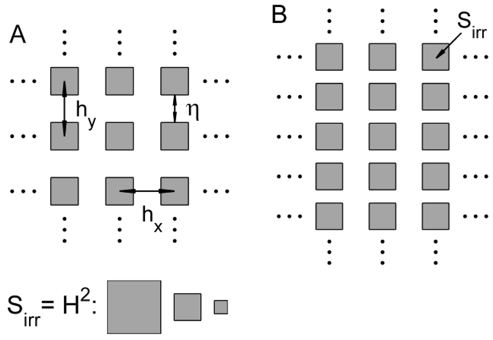
RDS writing was performed according to patterns with different periodic arrangements of irradiated zones in the shape of squares. In the study, from pattern to pattern, the square area of
Sirr =
H2 changed, where
H is the side of the square.
H could take values of 1 μm, 0.5 μm, and 0.25 μm (hereafter large, medium and small squares, respectively). The locations of the squares relative to each other in the patterns are shown schematically in
Figure 1. The intervals between the squares are marked as
hx and
hy. The directions of the
x- and
y-axes in the patterns were as close as possible to the directions of the crystallographic axes
X and
Y on the −
Z surface of LN. The total size of each pattern was ~200 × 200 μm
2. The writing of patterns with different configurations was carried out on the same sample in the same experiment, which allowed comparing the results obtained under the same conditions.
Scheme A in
Figure 1 corresponds to patterns with squares located in the nodes of an equilateral grid, i.e., when
hx =
hy =
h. As the sides of the squares increased, so did the intervals
h used in e-beam writing. For the small, medium, and large squares, the interval
h was 1 μm, 1.5 μm, and 2 μm, respectively. Thus, the distance between the edges of the squares (η) was equal to 1 μm for the medium and the large squares. For the small squares, η was equal to 0.75 μm.
Scheme B in
Figure 1 answers to patterns formed when
hx is fixed but when
hy gradually decreases, i.e., when
hx =
h and
hy <
h, the values of η along the
y-axis decreased from pattern to pattern up to zero.
The domain structures formed by Scheme A were compared with those obtained using Scheme B.
Of the known methods [
23,
24,
25] that are used to study ferroelectric domains, the method of selective or so-called differential etching was used in this work. The method is based on the different etch rates for the positive and negative ends of ferroelectric dipoles [
23,
24,
26]. Successful selective etching is a very strong argument for the existence of a domain pattern. Therefore, differential etching is used frequently, including in LN. For selective etching of domains in LN in recent years, acid HF or a mixture of acids HF and HNO
3 has been used [
27]. It should be added that no domain switching was observed as a result of treatment of the LN surface with acids HF or HF + HNO
3 at room temperature. This method is valid, simple, and characterizes the size and shape of the domains quite accurately [
28]. The achievable lateral resolution in selective etching is limited by the so-called lateral etch when the non-polar faces of the crystal (
Y) are also attacked. However, the etching of the side faces is slower due to some differences in the
X,
Y and
Z faces [
29] and becomes important when the etching time increases to several hours [
30].
In the present research, selective etching of e-beam domains in all irradiated patterns was performed in HF acid at room temperature for 30 min. Since, as mentioned above, different types of structures were placed on the same sample, the etching of all domains was performed simultaneously, i.e., under identical conditions. This increases the reliability of the detected morphological distinctions between domains in different structures.
Experiments with etching of samples were usually performed a few days after writing, therefore only relatively stable domains that escaped decay during this time were actually studied. The shapes of the upper part of the domains and their heights after etching were studied using an AFM (home-made, Chernogolovka, Russia) in contact mode. The overall regularity in the arrangement of the domains throughout the writing region was assessed by optical methods in an interference microscope (Axioplan 2, Carl Zeiss, Jena, Germany).
In addition to studying the peculiarities of the domain shapes, etching allowed estimating the position of the domain vertices relative to the original surface of the samples. For this purpose, their height measured by AFM was compared with the thickness of the removed surface layer, which, in turn, was found based on the value of the etch rate in HF the −
Z surface of the samples used. The etch rate, previously measured in Ref. [
31], is
Vetch = 14.4 nm/min, which is close to the Ref. [
27] data.
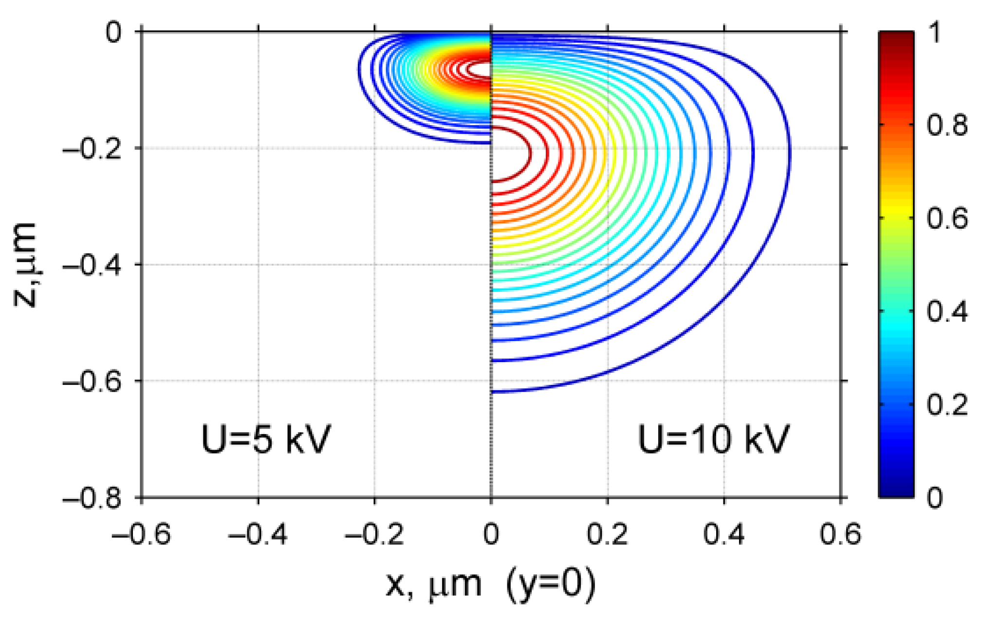
Experimental results were compared with calculations of the electric field distribution created by injected charges under different irradiation schemes. Data obtained using the Monte Carlo method were applied to set the distributions of injected charges (see Refs. [
18,
21] for details).
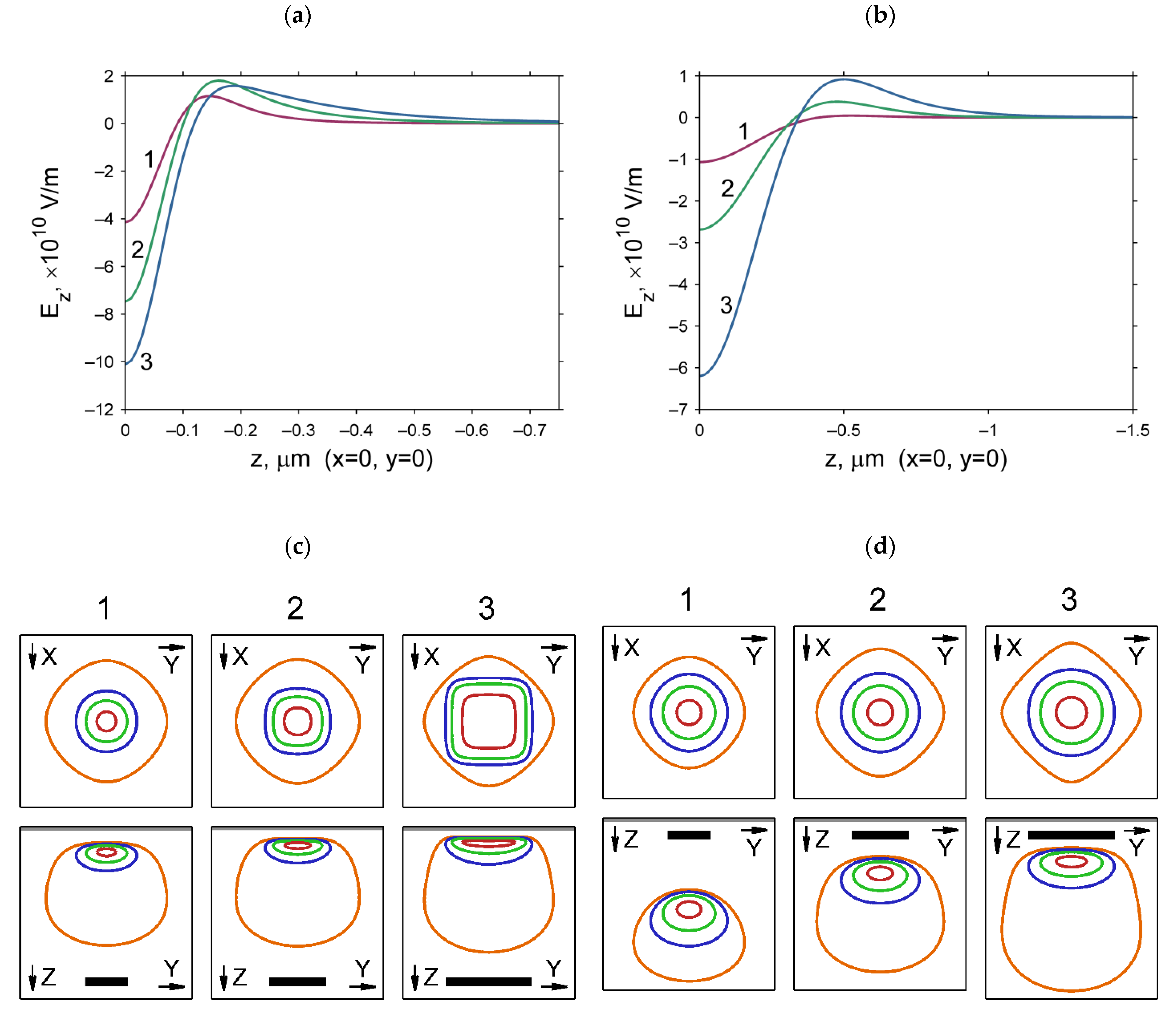
Figure 2 shows an example of the calculated injected charge distributions for Scheme A at
H = 0.25 μm and accelerating voltages of 5 kV and 10 kV.
The distributions of the electric potential ϕ were determined by numerically solving the Poisson equation in a small rectangular region located around one of the irradiated squares and with lateral dimensions
hx ×
hy. As was shown in Ref. [
21] Appendix B, in the case of EBDW-Me and at the used values of accelerating voltages, such a simplification, significantly reducing the computational cost, nevertheless allows revealing with sufficient accuracy the features of the electric field in each of the considered patterns.
The change in the domain distribution of the samples under study is due to the behavior of the normal component of the electric field strength vector (
Ez). It was demonstrated in Refs. [
18,
21,
31] that the appearance of domain structures correlates well with the location of zones where the
Ez vector reaches sufficiently large absolute values (exceeds by about two orders of magnitude the coercive field in LN, (
Ec = 2.2 × 10
7 V/m, Ref. [
32]) and is directed opposite to the vector of spontaneous electric polarization
Ps. Moreover, for the regular formation of domains, not only the values achieved in these zones are important but also the similar regular changes in
Ez within and outside these zones. Therefore, when comparing experimental data and simulation results, attention will be paid to both the maximum values of
Ez and the configuration of its distributions.
4. Discussion
It is reasonable to analyze the experimental results by comparing them with the data obtained by modeling the electric field distributions created by the injected charges under different irradiation options. Such consideration can help in identifying regularities that describe the formation of domains during EBDW-Me. Obviously, these regularities must be due to changes in the distribution of the injected charge when the accelerating voltage changes from 5 kV to 10 kV and when both the size and the mutual arrangement of the irradiated squares are varied. These changes, in turn, cause a restructuring of the distribution of the normal component of the electric field strength vector Ez, which controls the process of domain formation.
The results in
Table 1 show that the regular domains at EBDW-Me are successfully formed according to the arrangement of squares in the patterns under the action of very high field levels of 10
9–10
10 V/m (this is about two orders of magnitude higher than the value of
Ec). These values are comparable to the domain nucleation field under the high-voltage AFM tip [
34] and in the standard e-beam writing method without a top metal coating [
18,
31]. Decreasing
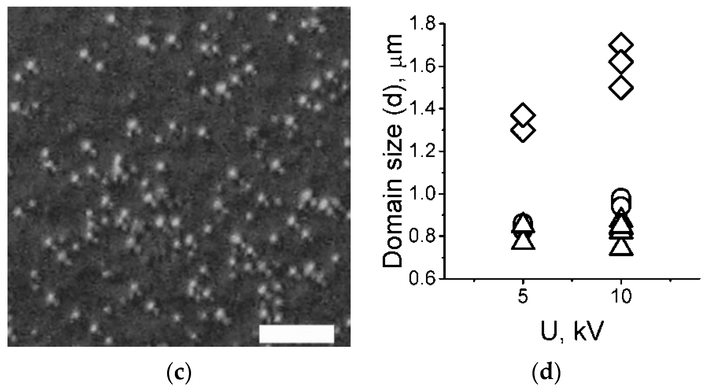
U from 10 kV to 5 kV expectedly reduced the diameter of the writable domains, which were almost oval-shaped in the optical images. The minimum size achieved corresponded to the domain diameter of 0.7–0.8 µm (
Figure 3d). However, when the size of irradiated squares is further reduced
H from 0.5 µm to 0.25 µm, the RDS writing is violated not only for 10 kV but also for 5 kV (
Figure 3c). See also Ref. [
21].
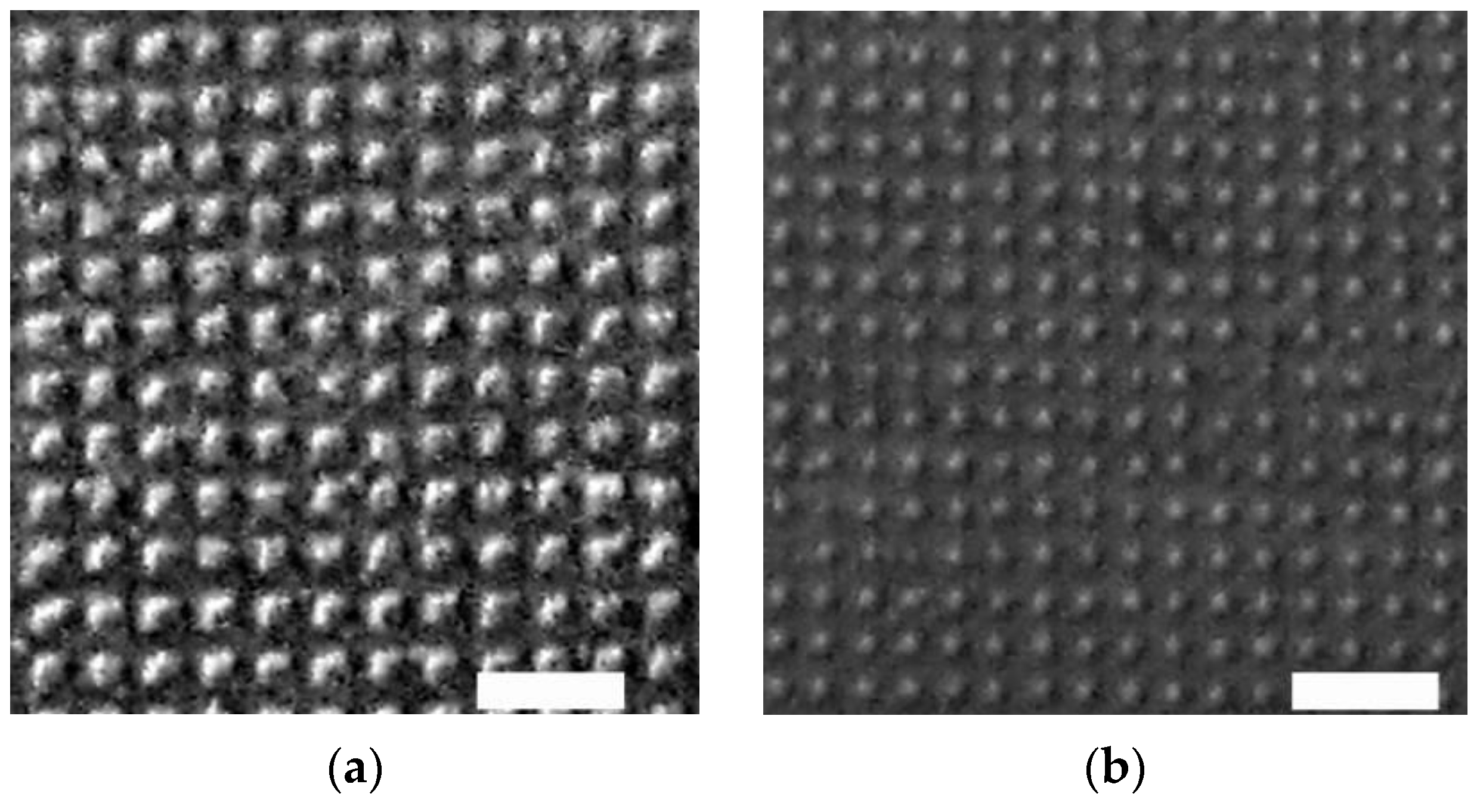
A distinctive feature of the submicron domains written at EBDW-Me was the needle-like vertexes. (
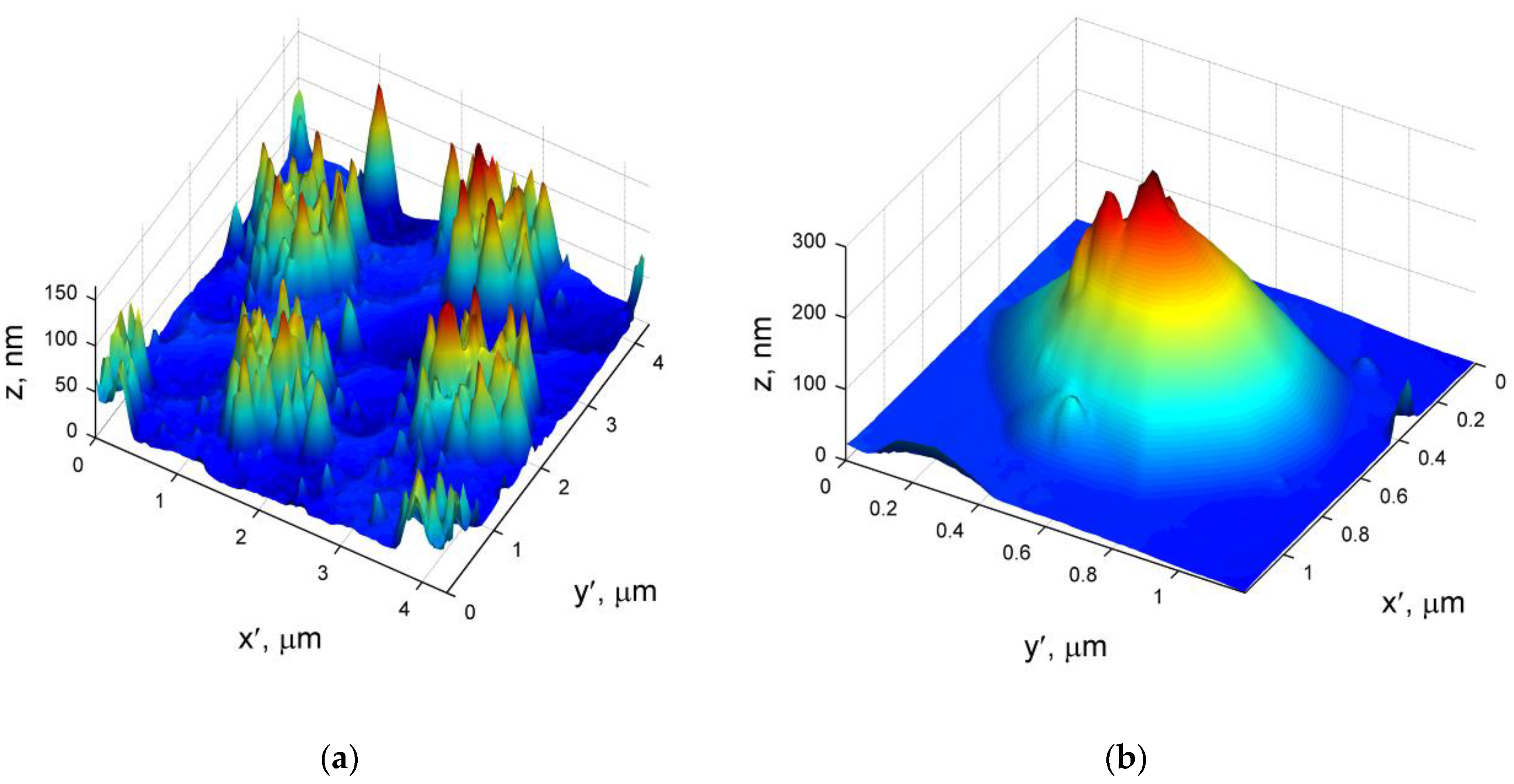
Figure 4). It should be noted that the needle-like vertices found in the submicron domains in this study differ significantly from the nearly flat submicron domains created by contact-field methods also revealed by differential etching [
35,
36]. Increasing the size of the irradiated squares under comparable irradiation conditions increased the probability of recording RDS but significantly altered the needle-shaped structure of the upper part of the larger domains (
Figure 4).
As shown in AFM profiles, the domain vertices at EBDW-Me are deepened relative to the irradiated surface similar to what is observed at EBDW at 15 kV [
31]. The deepening of the main part of the +
Z domains emphasizes also the fact that the AFM images sometimes show single very high domains (see
Figure 6d,g). The height of these very high domains (400–450 nm) is comparable to the thickness of the −
Z layer removed by etching for 30 min. Perhaps, in some anomalous zones, the nucleation of individual domains can occur much closer to the surface. Typically, the average height of the domains in the AFM profiles is ~150–200 nm for both applied accelerating voltages, despite the considerable differences in the injected charge distribution (see
Figure 2). The deepening of the nucleation zones is also well illustrated by the electric field distributions.
Figure 5 shows that it can be more significant at 10 kV compared to 5 kV. Apparently, the accuracy of both the calculated and experimental methods is not sufficient to reveal real differences in the degree of domain deepening at relatively low
U. In addition, it should be noted that there is indirect evidence for the existence of some disturbed surface layer in LN crystals [
37,
38]. It can be assumed that in this layer, the conditions of domain nucleation may differ from the bulk ones. This may also smooth out the effect of differences in the distributions of the injected charges at 5 and 10 kV on the domain deepening.
Below, the morphology of the domains is discussed in detail in the context of the field configuration peculiarities under the irradiated squares at Scheme A.
Figure 5 demonstrates that when using Scheme A, the lateral dimensions of the
Ec-zones do not exceed the dimensions of the
hx ×
hy regions around the irradiated squares. Thus, it can be assumed that in the case of Scheme A, for all values of
H in the formation process, the domains do not have a noticeable influence on each other. Comparing the
Ec-zones calculated at different
U, it can be observed that their size (especially vertically, see the
Lc values in
Table 1) increases with voltage growth in the variants with both the large and the medium squares. This is obviously due to the already mentioned difference in the size and the position of the injected charge regions at 5 kV and 10 kV (see
Figure 2, for example). The difference in the size of the
Ec-zones is much more significant at
H = 1 μm. A similar trend can be detected when comparing the dimensions of the domains presented in
Figure 3d (see also Ref. [
21]).
The different size of the injected charge regions at 5 kV and 10 kV also affects the δ values—the average excess of the sizes of regular domains
d over
H. At 10 kV this excess is much greater (see
Table 1). In addition, the behavior of δ agrees well with the different characters of the dependence
(
H) at various
U. As
H increases, δ decreases at 5 kV and grows at 10 kV (
Table 1).
Comparison of the configuration of the calculated Ez distributions and the morphology of the domains allows for identifying some regularities of their formation at EBDW-Me.
At
H = 1 μm and
U = 5 kV in the distribution of
Ez the 0.3
-zone is close in shape to the irradiated square (
Figure 5c). From the optical and AFM images, it follows that the domains at such irradiation parameters are also formed within regions with a square shape (
Figure 3a and
Figure 4a). Hence, it can be concluded that the 0.3
-zones appear to be the most significant for domain generation when EBDW-Me is applied. A comparison of
Figure 4a and
Figure 5c suggests that simultaneous nucleation of a large number of domains must occur in a region with a very high electric field strength
Ez ≥ 0.9
(further 0.9
-zone). This region is smaller than the 0.3
-zone but still quite extensive. In addition, the graph in
Figure 5a shows that at the above parameters,
Ez decreases slowly enough in depth after reaching the maximum. Such conditions can contribute to the rapid frontal growth of domains and their acquisition of the form of peaks with a large steepness of the walls, due to which the joining of these domains occurs rather deeply.
Reducing
H to 0.5 μm while maintaining the value of the accelerating voltage significantly changes the distribution of
Ez (
Figure 5c). The 0.9
-zone noticeably decreases in size. Additionally, there is a faster decay of
Ez after the point
(
Figure 5a) and the 0.3
-zone takes on a more rounded shape. All this may explain why, in this case, domains are generated in the form of pyramids with sloping walls and an almost oval base, and why these domains are crowned by only one or two needle-like vertices (
Figure 4b).
As already indicated, the patterns with the small squares arranged in Scheme A did not allow for obtaining RDS at any of the voltages used (see, for example,
Figure 3c). The reason for this is a violation of the conditions that guarantee the successful formation of regular domains at EBDW-Me. These conditions were previously established in Ref. [
21] and consist of the need for a combination of very high field strength (
≥ 10
9 V/m) and vertical size of the
Ec-zones of the order of 1 μm. According to
Table 1,
Figure 5c,d at 5 kV one of these requirements is not met, and at 10 kV both are not satisfied. As explained in Ref. [
21], violation of these requirements does not allow for the formation of sufficiently large domains capable of resisting back-switching under the action of depolarizing fields. Domains that reach certain critical sizes are known to be more successful in keeping their stability over long periods of time [
39,
40].
At the same time, when passing to writing in Scheme B, in spite of the detected decrease in the field when the injected charges approach each other (
Table 2), the experimental results demonstrate the possibility to write regular domain structures in the form of stripes not only when using the large and the medium squares, but also the small squares. A comparison of the results of calculations and experiments showed that to increase the stability of small-sized domains, it is sufficient to bring the irradiated squares closer to the contact of 0.3
-zones. The AFM images (
Figure 6) clearly show that this convergence of the squares results in the merging of the lower parts of the submicron domains. However, at 10 kV, it was necessary to quadruple the irradiation dose due to a very low value of
at the original value of 5000 µC/cm
2 (see
Table 2) to obtain the desired result.
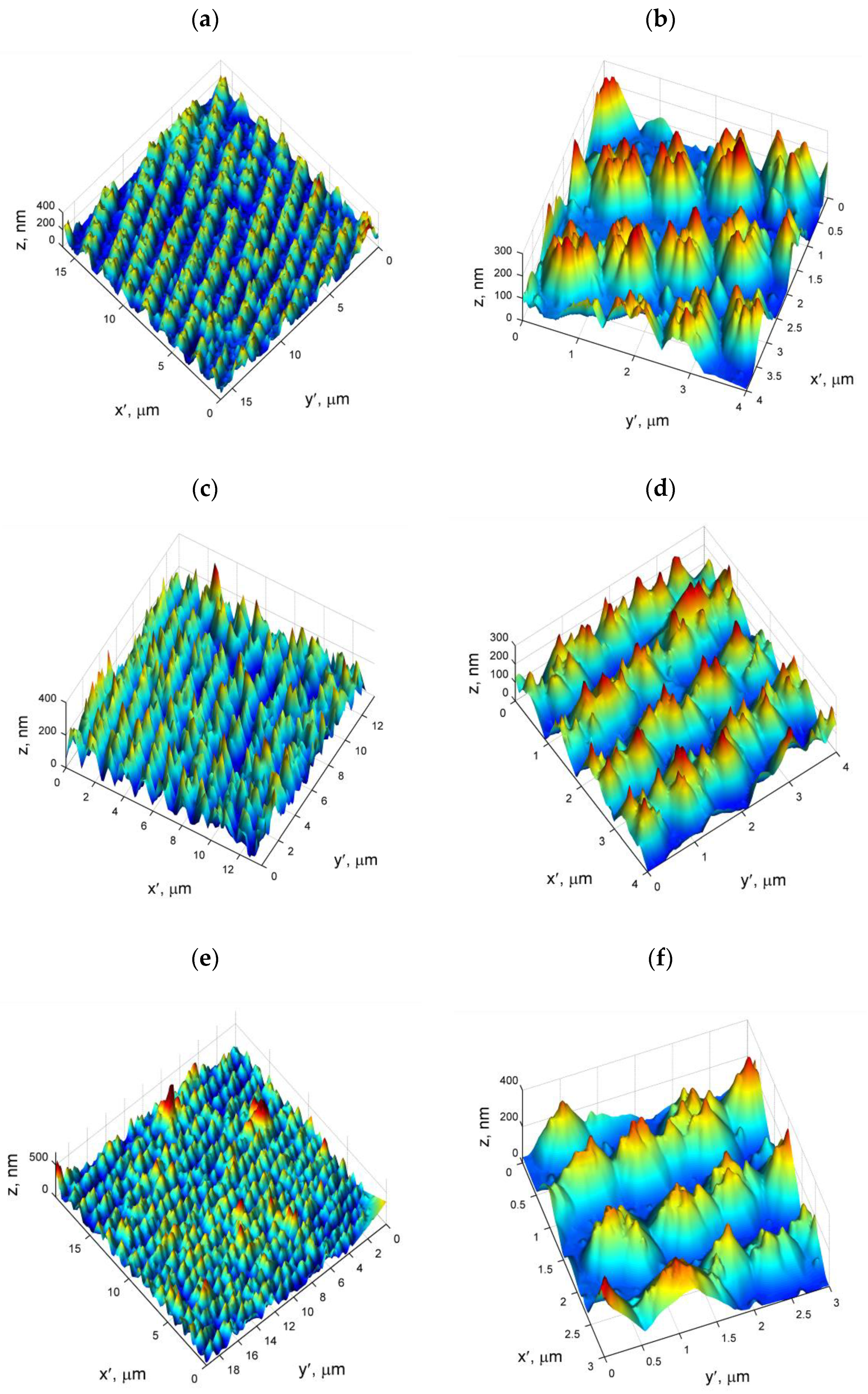
The characteristic changes detected in the AFM images obtained for Scheme B, in contrast to Scheme A, include an increase in the number of needle-like vertices at the domains for both the medium and the small squares. Numerous such vertices are distributed rather chaotically within domain aggregations and their presence seems to indicate an increase in the amount of merged small domains, which were previously unstable and disappeared. As the nucleation sites come closer together, these domains, which grow frontally inward, merge with each other in their lower part and acquire cooperative resistance to back-switching.
Slightly different changes in domain morphology are found in the 0.3
-zone merging for the large squares. In this case, apparently due to the decrease in
(
Table 2), the regions covered by narrow domains (~100–200 nm wide), which merged only at a fairly great depth, transformed into denser micron-sized aggregations (cf.
Figure 4a and
Figure 6b). These aggregations are shaped like truncated pyramids, with several short peaks retained in their upper part. In the lower part of these somewhat rounded pyramids, narrow isthmuses connecting these pyramids can be seen.
In the upper part of all domains obtained by Scheme B, chains of sharp vertices are formed, which seems to be due to the lack of merging of the 0.9
-zones at the selected values of
hy. Given some deepening of these +
Z domain vertices relative to the irradiated surface and a rather large tilt angle of the domain walls relative to the polarization direction, it can be assumed that these regions may exhibit special properties inherent to charged domain walls [
41].
Analysis of the AFM images also allows concluding about a decrease in the lateral size of the domains in the transition to Scheme B from Scheme A. Inclined and, therefore, charged domain walls start to electrostatically repel each other as they become closer, preventing domain growth in breadth. A similar proximity effect between domains was found earlier in Ref. [
42]. The results obtained in Ref. [
21] showed that the decay or stability of EBDW-Me RDS written using small accelerating voltages and squares with
H = 0.25 μm are governed by the competitive interaction of electrostatic repulsion between the walls of the nearest submicron domains and the convergence of injected charges, leading to the formation of extended zones with an electric field of sufficient strength. The formation of such zones helps to overcome the repulsion of the domain walls and, consequently, results in domain merging.
5. Conclusions
This article investigates the morphology of domains that nucleate near the surface –Z cut of lithium niobate with a ground metal coating and irradiated with an electron beam at accelerating voltages of 5 kV and 10 kV. The consideration is based on the comparison of optical and AFM images of the obtained domains with data for modeling the spatial distribution of the field of charges injected during irradiation. When creating the test structures (each with a total size of ~200 × 200 μm2), patterns were used in which the locally irradiated regions (squares) were placed in the nodes of a rectangular grid. The side of the squares could take values of 0.25 μm, 0.5 μm, and 1 μm.
It was found that the shape and lateral dimensions of the domains, as well as the correspondence of the writing results to the applied patterns, significantly depend on the magnitude of the accelerating voltage, as well as on the size of the squares and the distance between them. A decrease in the accelerating voltage led to an increase in the maximum values of the normal component of the electric field strength vector Ez, whose behavior determines changes in the domains. Reducing the size of the squares in the patterns could cause a decrease in Ez. Therefore, varying these two parameters by changing the magnitude of the field strength, as well as its distribution, made it possible to influence the success of the electron beam writing in general and the morphology of the obtained domains in particular.
An unusual feature of the shape of the domains nucleated under the metal was the appearance of needle-like vertices of nanometer size. The domains were deepened relative to the irradiated surface. The minimum lateral size of the separately located domains, resistant to back-switching under the given experimental conditions, corresponded to ~0.7–0.8 µm. Smaller submicron domains became stable only after merging with each other.
At the least squares, stable domain structures were formed only when these squares strongly converged along one of the grid directions used in the patterns. Note that a chain of needle-like vertices remaining from the merged domains was preserved in the upper part of the linear domain structures formed in this case. At the medium-sized squares, stable domains had the form of pyramids with needle-like vertices and with a base close to a hexagon or an oval. The lateral dimensions of the pyramids were about or less than a micron. With the large squares in the irradiation zones, many stable sharp-angled domains of ~100–200 nm width were formed, merging at a certain depth.
The presented studies of morphological changes in the LN domains can be useful for understanding the domain formation processes in electron-irradiated surface layers of ferroelectric materials in contact with a grounded metallic film. The study of the influence of irradiation conditions on the features of the forming domains is an urgent task due to the increasing use of domain structures of different types in a variety of practical applications, for instance, in photonics technology, in generating high-power laser radiation, in optical communications, and in information storage and processing.


