
Growth of Carbon Nanotubes on Diamond with a Robust Structural Connection via Microwave Plasma Chemical Vapor Deposition
Abstract
:1. Introduction
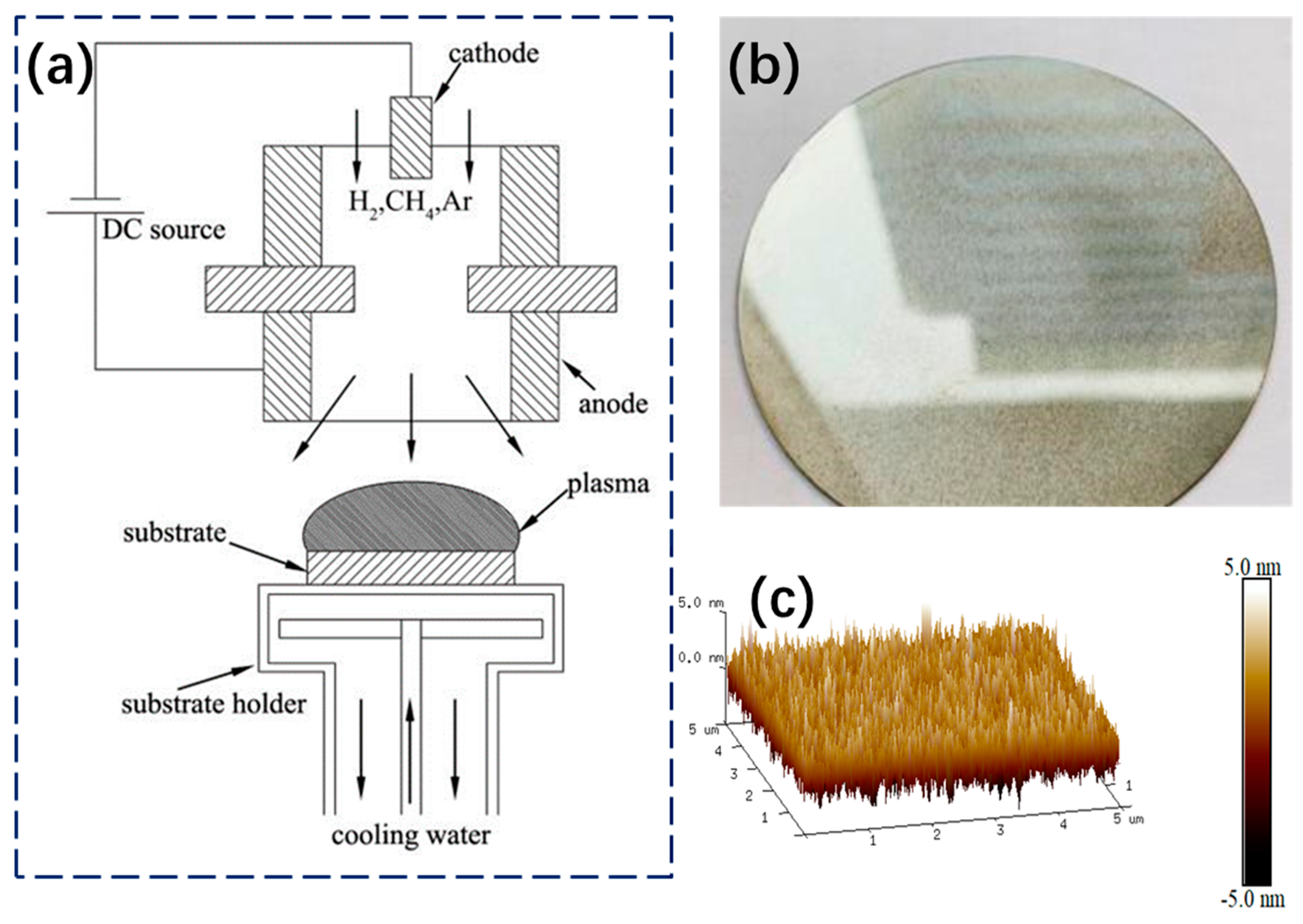
2. Experimental
2.1. Preparation of Substrates
2.2. Synthesis of Carbon Nanotubes
2.3. Characterization
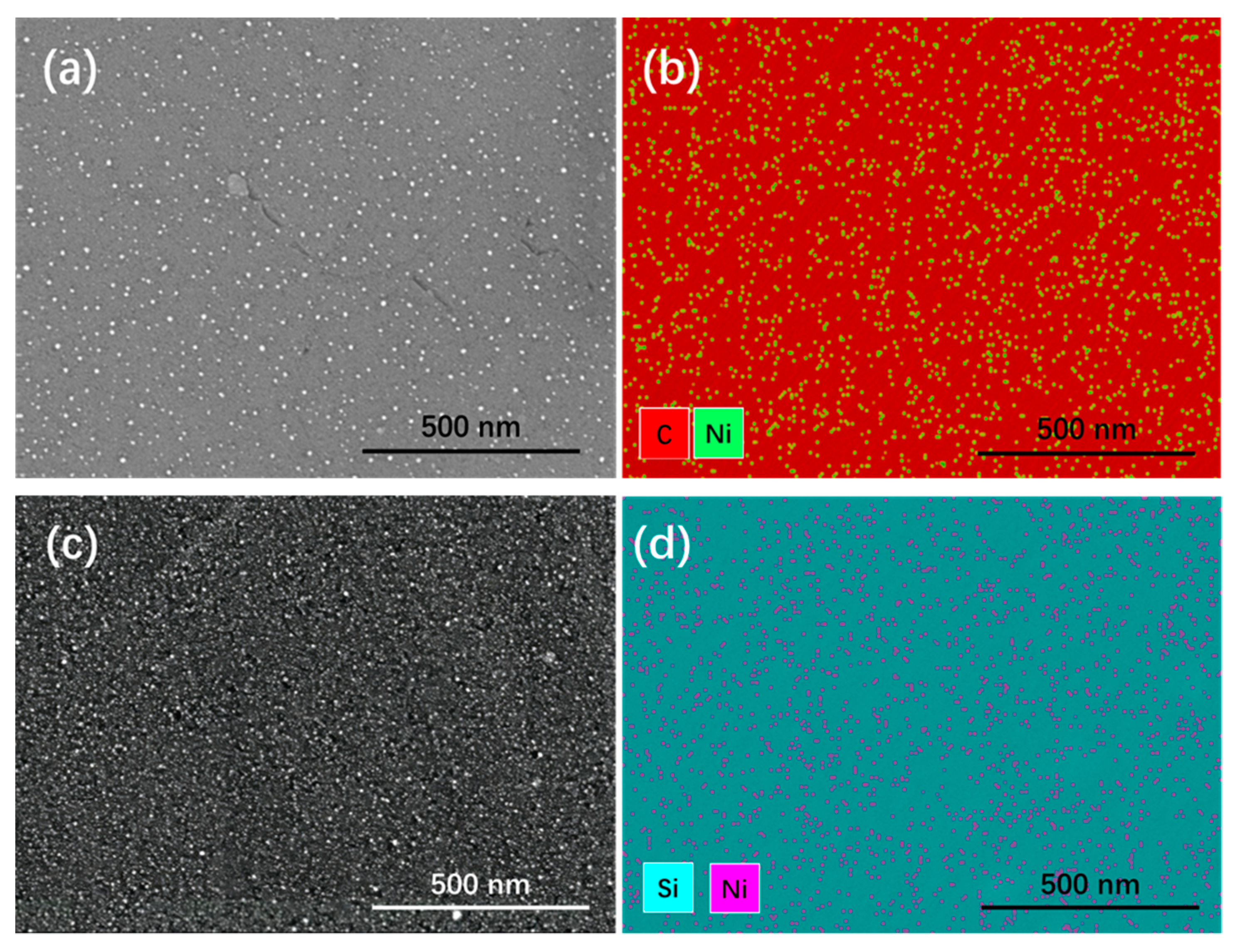
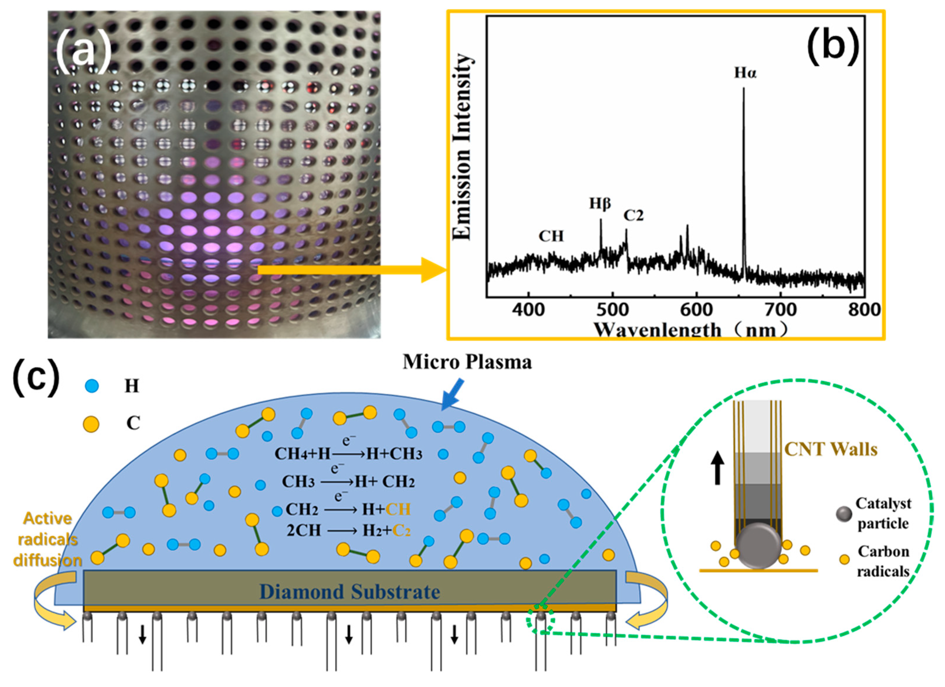
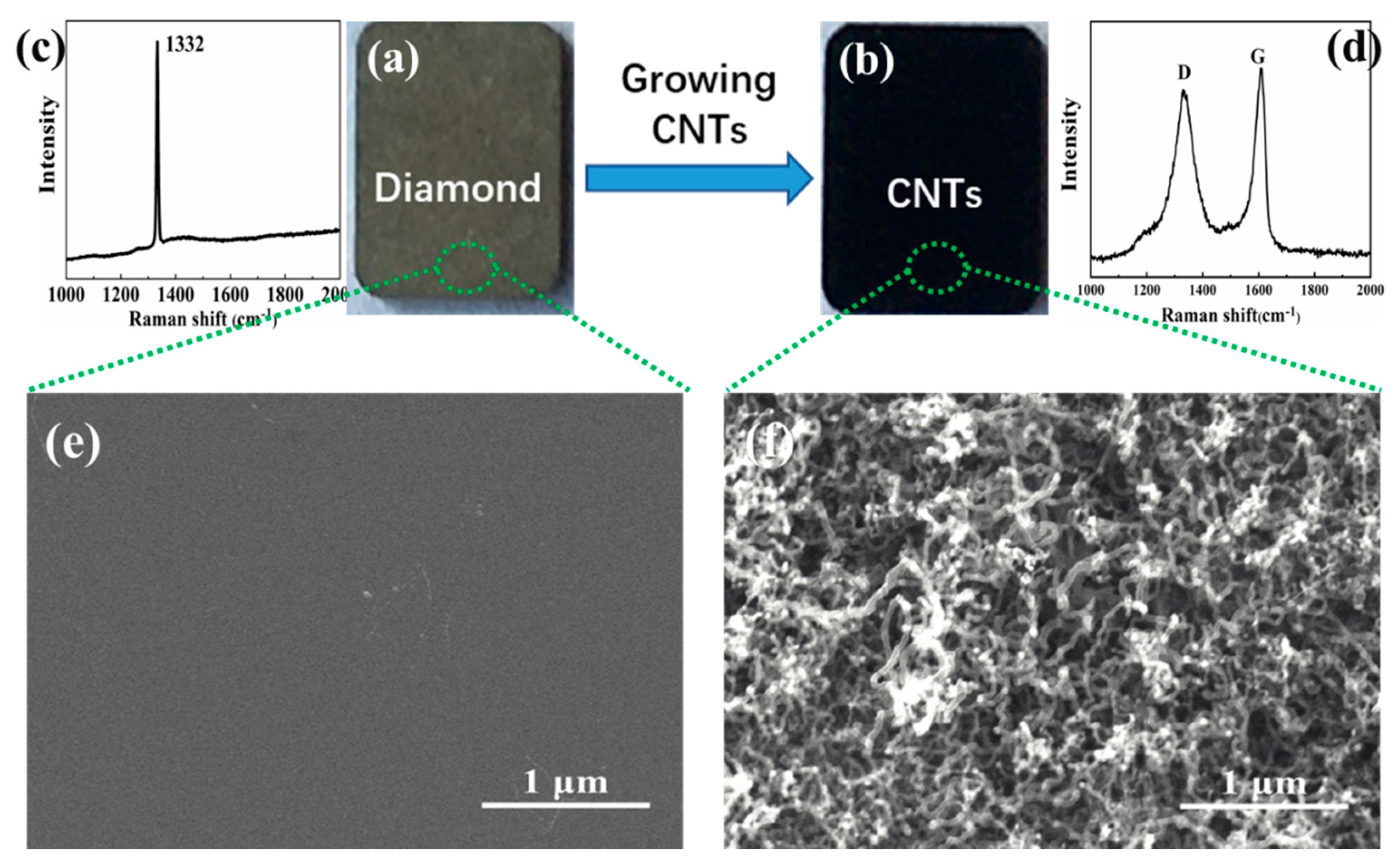
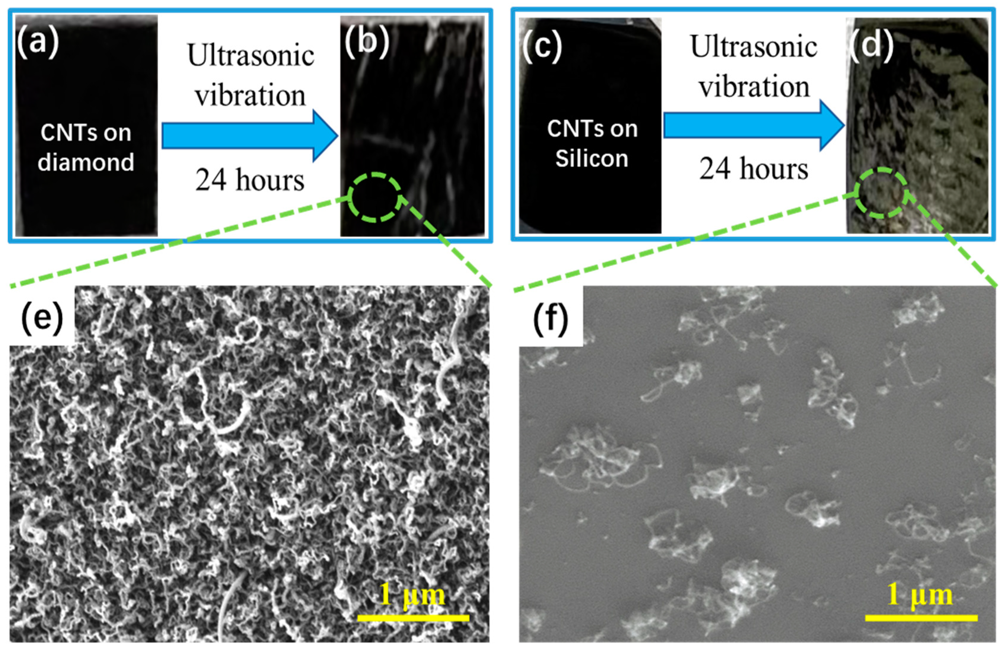
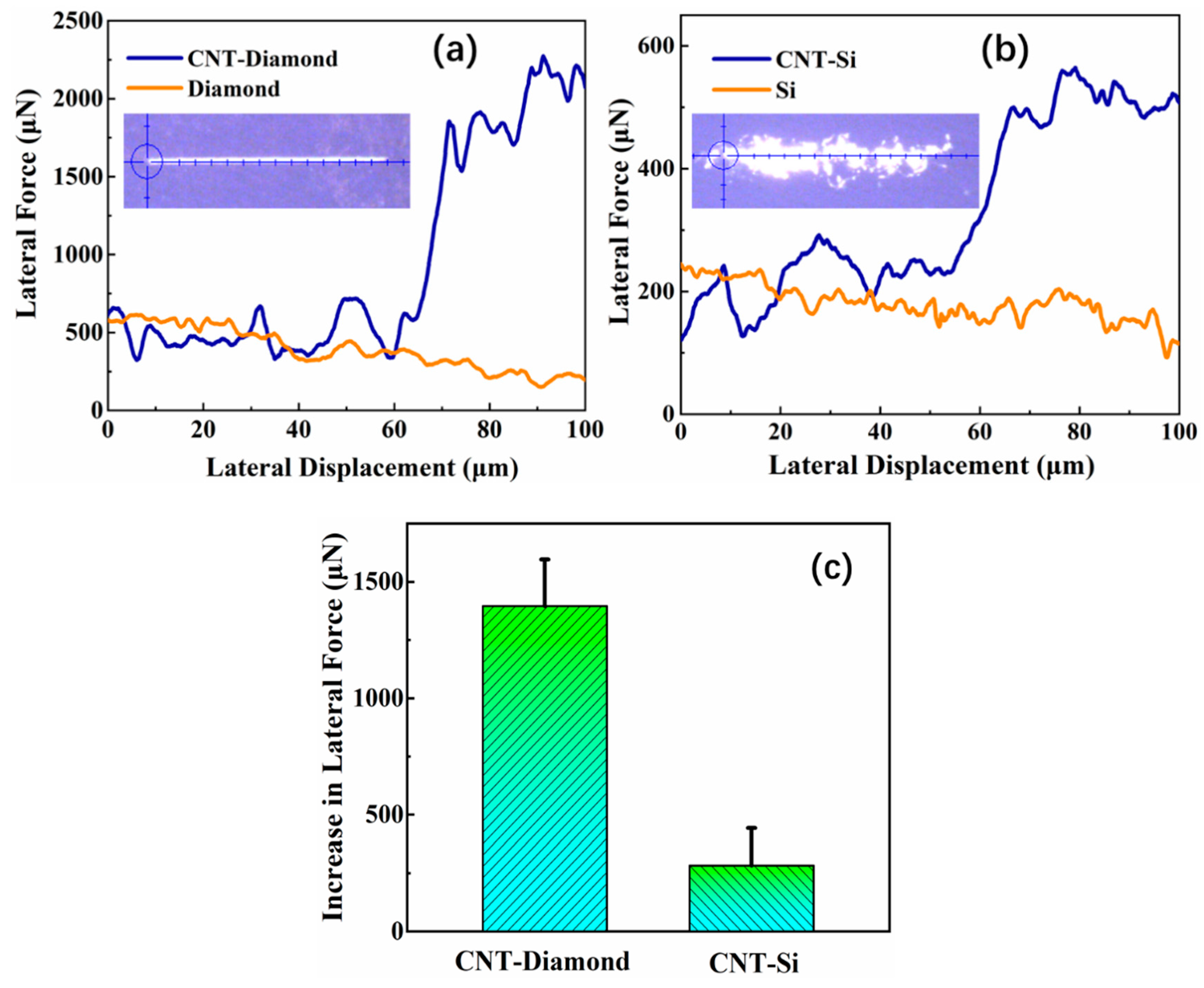
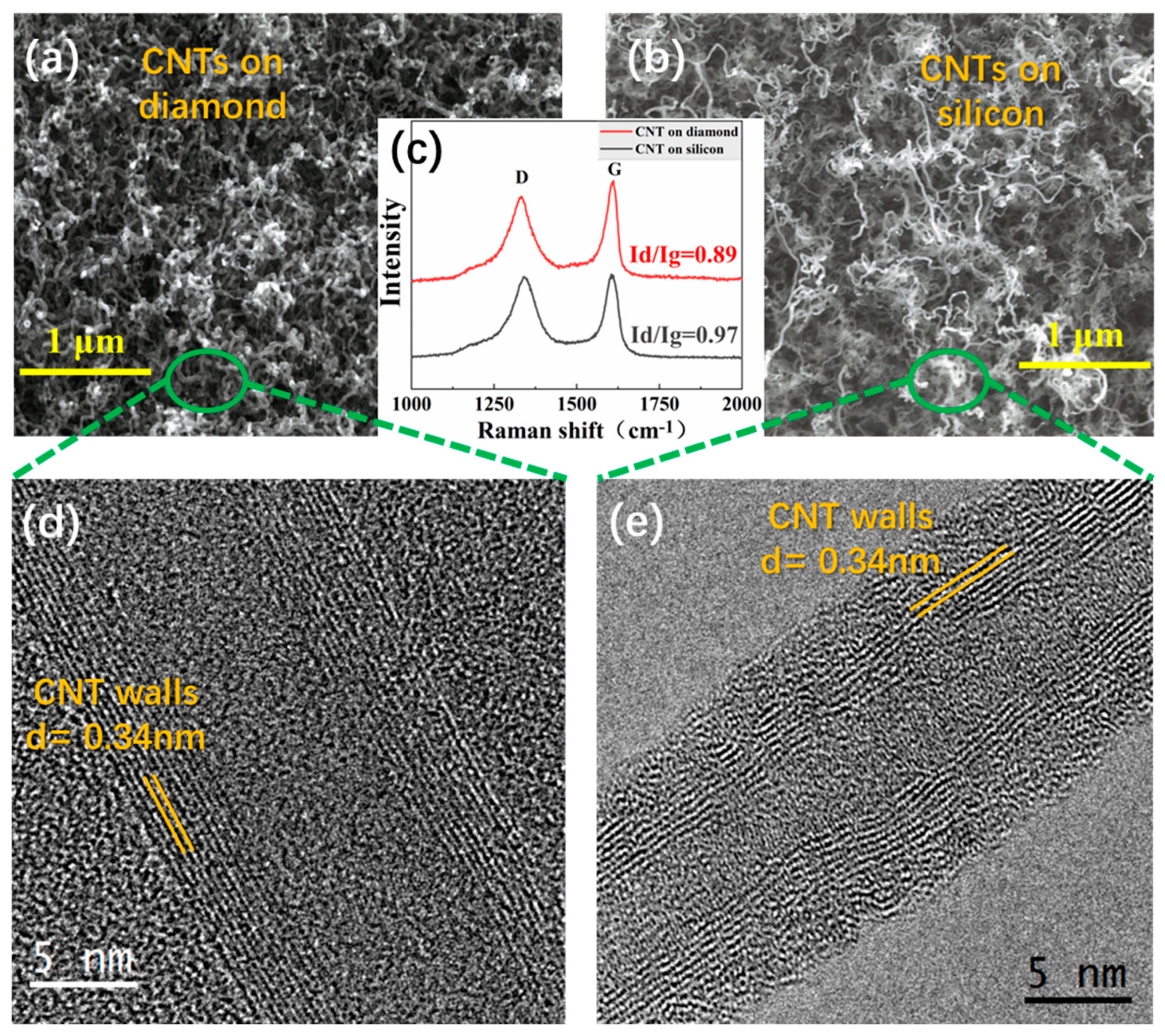
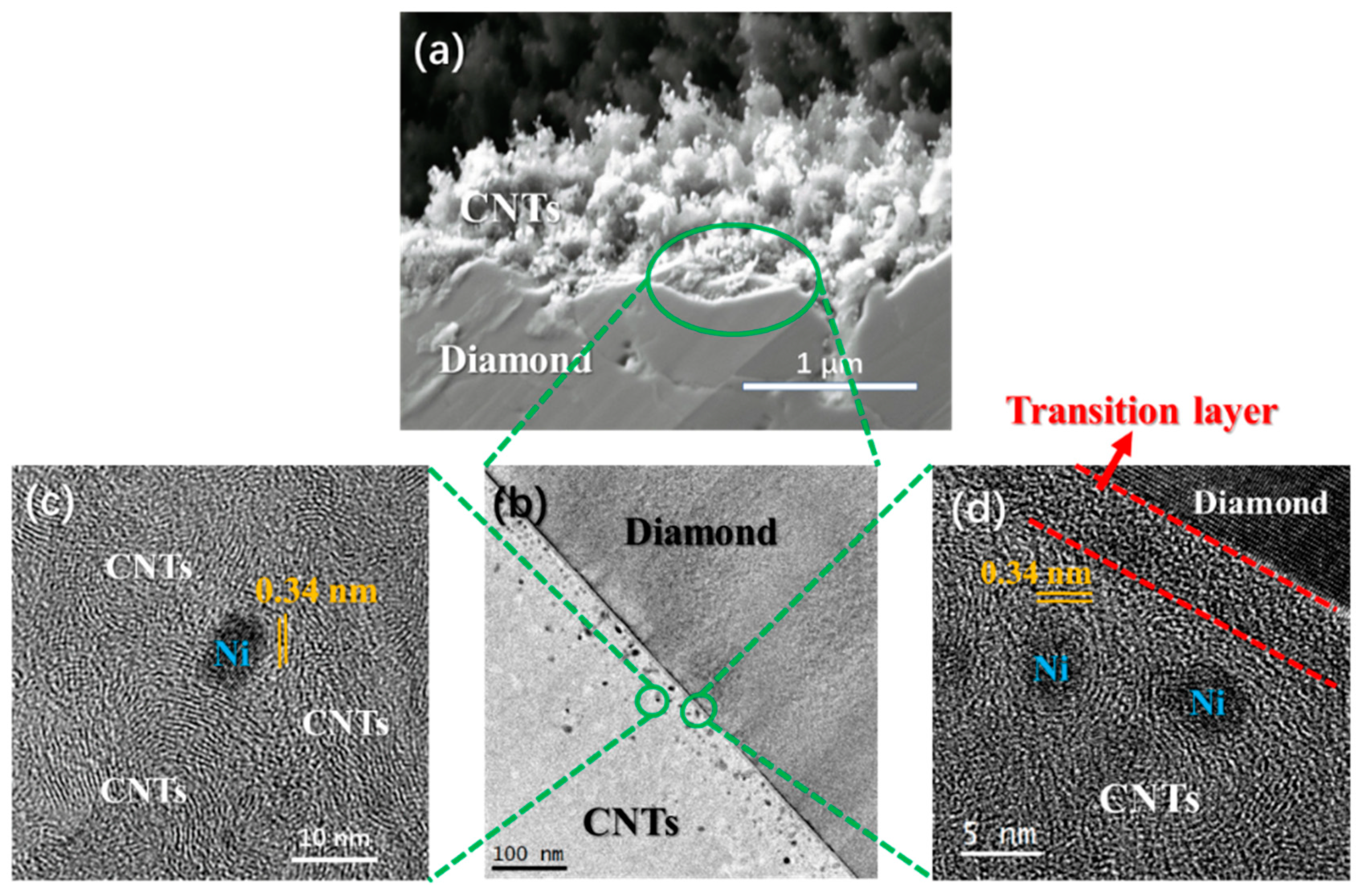
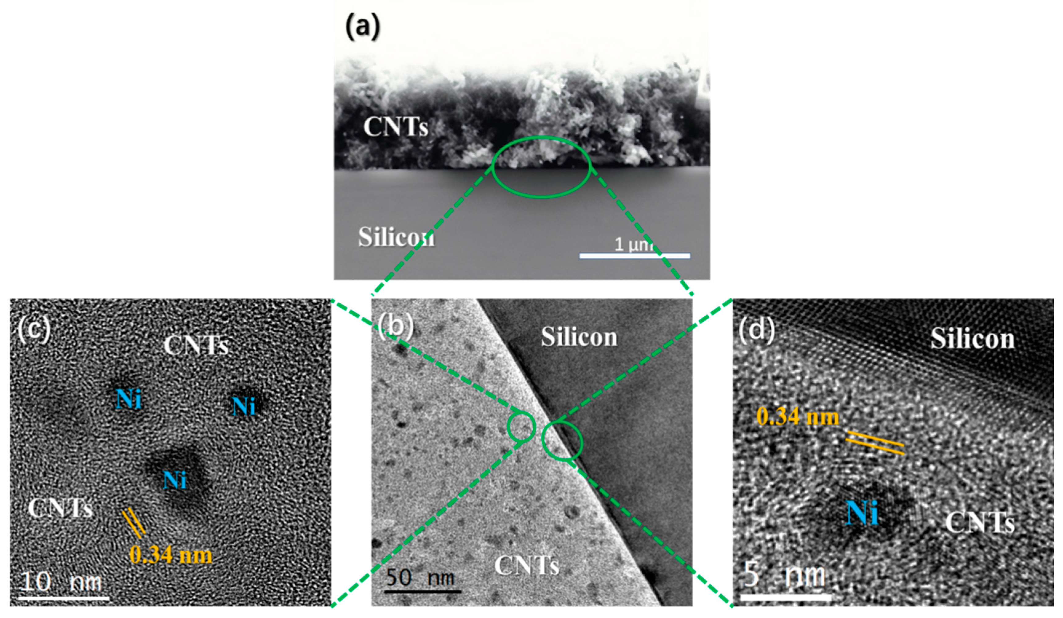
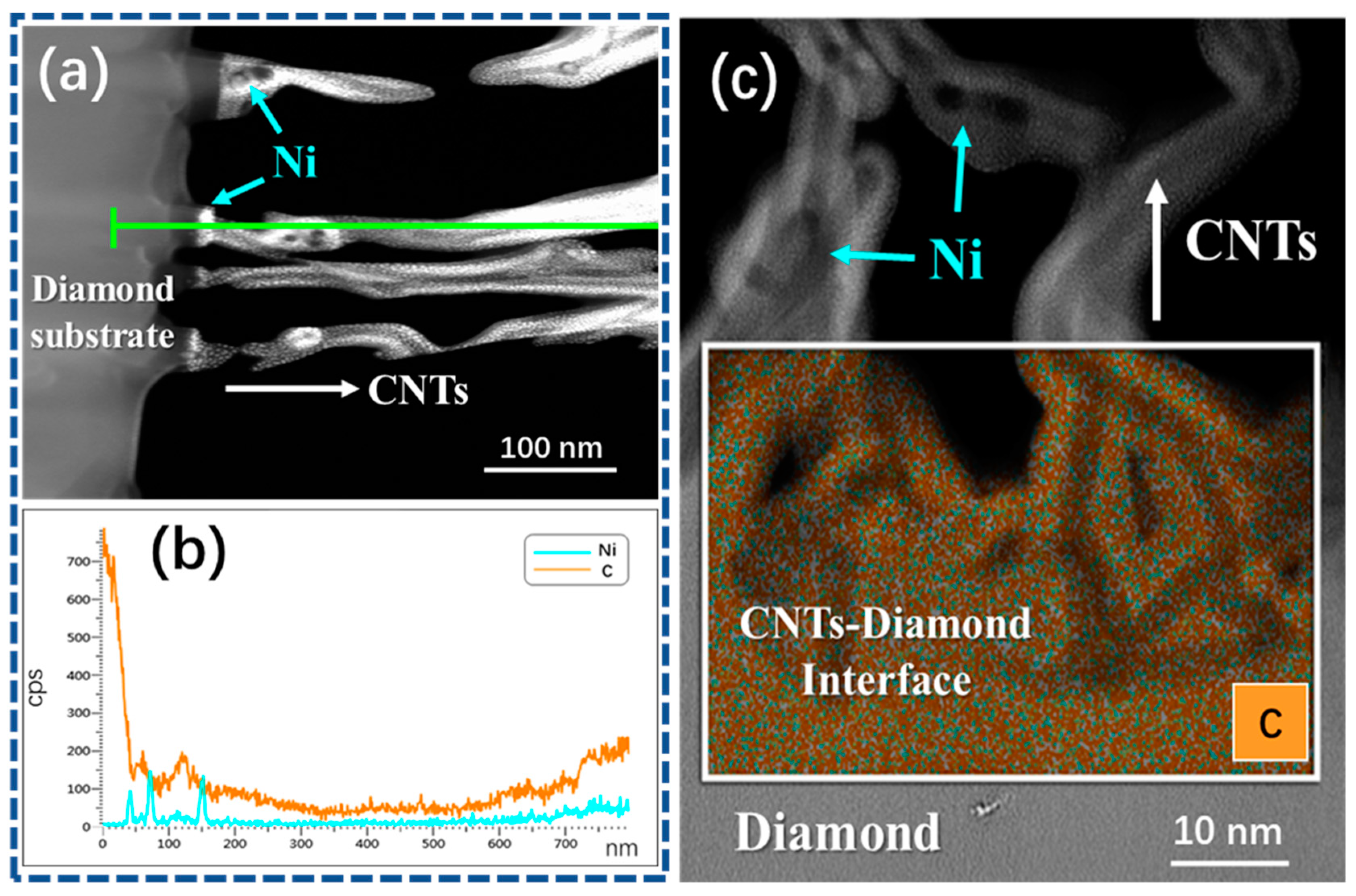
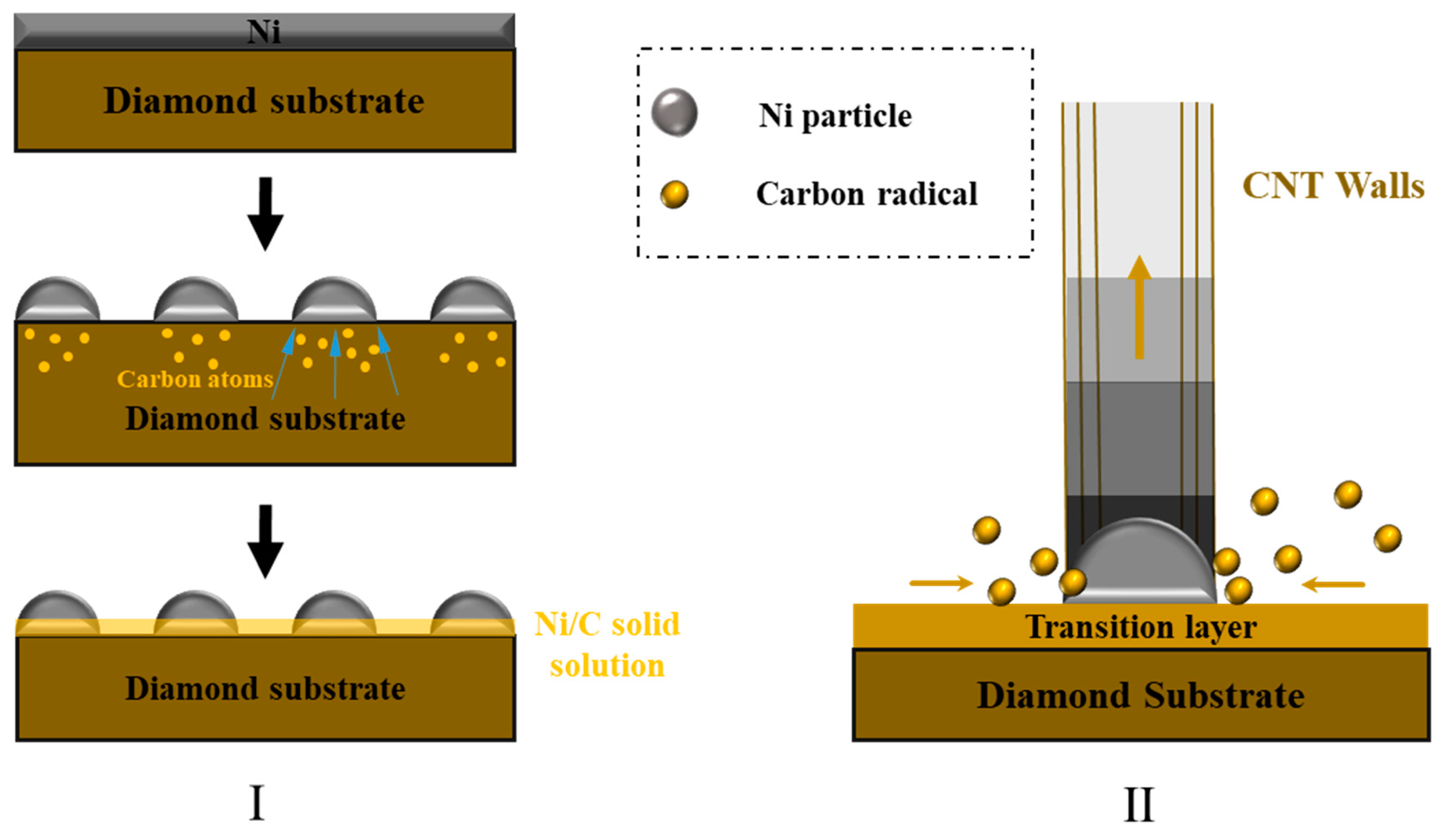
3. Results and Discussion
4. Conclusions
Author Contributions
Funding
Institutional Review Board Statement
Informed Consent Statement
Data Availability Statement
Conflicts of Interest
References
- Iijima, S. Helical microtubules of graphitic carbon. Nature 1991, 354, 56–58. [Google Scholar] [CrossRef]
- De Volder, M.F.; Tawfick, S.H.; Baughman, R.H.; Hart, A.J. Carbon nanotubes: Present and future commercial applications. Science 2013, 339, 535–539. [Google Scholar] [CrossRef] [PubMed] [Green Version]
- Lehman, J.; Yung, C.; Tomlin, N.; Conklin, D.; Stephens, M. Carbon nanotube-based black coatings. Appl. Phys. Rev. 2018, 5, 011103. [Google Scholar] [CrossRef] [Green Version]
- Li, S.; Ma, L.; Long, H.; Yu, X.; Luo, H.; Wang, Y.; Zhu, H.; Yu, Z.; Ma, M.; Wei, Q. Enhanced electron field emission properties of diamond/microcrystalline graphite composite films synthesized by thermal catalytic etching. Appl. Surf. Sci. 2016, 367, 473–479. [Google Scholar] [CrossRef]
- Yang, Z.-P.; Ci, L.; Bur, J.A.; Lin, S.-Y.; Ajayan, P.M. Experimental observation of an extremely dark material made by a low-density nanotube array. Nano Lett. 2008, 8, 446–451. [Google Scholar] [CrossRef]
- Mizuno, K.; Ishii, J.; Kishida, H.; Hayamizu, Y.; Yasuda, S.; Futaba, D.N.; Yumura, M.; Hata, K. A black body absorber from vertically aligned single-walled carbon nanotubes. Proc. Natl. Acad. Sci. USA 2009, 106, 6044–6047. [Google Scholar] [CrossRef] [Green Version]
- Holz, T.; Mata, D.; Santos, N.; Bdikin, I.; Fernandes, A.; Costa, F. Stiff diamond/buckypaper carbon hybrids. ACS Appl. Mater. Interfaces 2014, 6, 22649–22654. [Google Scholar] [CrossRef]
- Ebbesen, T.W.; Ajayan, P.M. Large-scale synthesis of carbon nanotubes. Nature 1992, 358, 220–222. [Google Scholar] [CrossRef]
- Prasek, J.; Drbohlavova, J.; Chomoucka, J.; Hubalek, J.; Jasek, O.; Adam, V.; Kizek, R. Methods for carbon nanotubes synthesis. J. Mater. Chem. 2011, 21, 15872–15884. [Google Scholar] [CrossRef]
- Koziol, K.; Boskovic, B.O.; Yahya, N. Synthesis of carbon nanostructures by CVD method. In Carbon and Oxide Nanostructures; Springer: Berlin, Germany, 2010; pp. 23–49. [Google Scholar]
- Shah, K.A.; Tali, B.A. Synthesis of carbon nanotubes by catalytic chemical vapour deposition: A review on carbon sources, catalysts and substrates. Mater. Sci. Semicond. Process. 2016, 41, 67–82. [Google Scholar] [CrossRef]
- Joselevich, E.; Lieber, C.M. Vectorial growth of metallic and semiconducting single-wall carbon nanotubes. Nano Lett. 2002, 2, 1137–1141. [Google Scholar] [CrossRef]
- Uh, H.S.; Lee, S.M.; Choi, S.R.; Park, S.S.; Cho, E.S.; Lee, J.D.; Kwon, S.J. Effect of plasma pretreatment on the structure and emission characteristics of carbon nanotubes. J. Korean Phys. Soc. 2003, 43, 924–929. [Google Scholar] [CrossRef]
- Kobashi, K.; Inoue, T.; Tachibana, H.; Kumagai, K.; Miyata, K.; Nishimura, K.; Nakaue, A. Selected-area deposition of diamond films. In The Physics and Chemistry of Carbides, Nitrides and Borides; Springer: Berlin, Germany, 1990; pp. 159–167. [Google Scholar]
- Talapatra, S.; Kar, S.; Pal, S.; Vajtai, R.; Ci, L.; Victor, P.; Shaijumon, M.; Kaur, S.; Nalamasu, O.; Ajayan, P. Direct growth of aligned carbon nanotubes on bulk metals. Nat. Nanotechnol. 2006, 1, 112–116. [Google Scholar] [CrossRef] [PubMed]
- Hata, K.; Futaba, D.N.; Mizuno, K.; Namai, T.; Yumura, M.; Iijima, S. Water-assisted highly efficient synthesis of impurity-free single-walled carbon nanotubes. Science 2004, 306, 1362–1364. [Google Scholar] [CrossRef] [Green Version]
- Cheung, C.L.; Kurtz, A.; Park, H.; Lieber, C.M. Diameter-controlled synthesis of carbon nanotubes. J. Phys. Chem. B 2002, 106, 2429–2433. [Google Scholar] [CrossRef]
- Murakami, T.; Sako, T.; Harima, H.; Kisoda, K.; Mitikami, K.; Isshiki, T. Raman study of SWNTs grown by CCVD method on SiC. Thin Solid Film. 2004, 464, 319–322. [Google Scholar] [CrossRef]
- Kumar, M.; Ando, Y. A simple method of producing aligned carbon nanotubes from an unconventional precursor–Camphor. Chem. Phys. Lett. 2003, 374, 521–526. [Google Scholar] [CrossRef]
- Colomer, J.-F.; Stephan, C.; Lefrant, S.; Van Tendeloo, G.; Willems, I.; Konya, Z.; Fonseca, A.; Laurent, C.; Nagy, J.B. Large-scale synthesis of single-wall carbon nanotubes by catalytic chemical vapor deposition (CCVD) method. Chem. Phys. Lett. 2000, 317, 83–89. [Google Scholar] [CrossRef] [Green Version]
- Willems, I.; Kónya, Z.; Colomer, J.-F.; Van Tendeloo, G.; Nagaraju, N.; Fonseca, A.; Nagy, J.B. Control of the outer diameter of thin carbon nanotubes synthesized by catalytic decomposition of hydrocarbons. Chem. Phys. Lett. 2000, 317, 71–76. [Google Scholar] [CrossRef]
- Ward, J.; Wei, B.; Ajayan, P. Substrate effects on the growth of carbon nanotubes by thermal decomposition of methane. Chem. Phys. Lett. 2003, 376, 717–725. [Google Scholar] [CrossRef]
- Ago, H.; Nakamura, K.; Imamura, S.; Tsuji, M. Growth of double-wall carbon nanotubes with diameter-controlled iron oxide nanoparticles supported on MgO. Chem. Phys. Lett. 2004, 391, 308–313. [Google Scholar] [CrossRef]
- Szabó, A.; Méhn, D.; Kónya, Z.; Fonseca, A.; Nagy, J.B. “Wash and go”: Sodium chloride as an easily removable catalyst support for the synthesis of carbon nanotubes. PhysChemComm 2003, 6, 40–41. [Google Scholar] [CrossRef]
- Bonard, J.-M.; Klinke, C.; Dean, K.A.; Coll, B.F. Degradation and failure of carbon nanotube field emitters. Phys. Rev. B 2003, 67, 115406. [Google Scholar] [CrossRef]
- Neves, A.; Nazaré, M.H. Properties, Growth and Applications of Diamond; IET: London, UK, 2001. [Google Scholar]
- Tong, T.; Zhao, Y.; Delzeit, L.; Kashani, A.; Meyyappan, M.; Majumdar, A. Dense vertically aligned multiwalled carbon nanotube arrays as thermal interface materials. IEEE Trans. Compon. Packag. Technol. 2007, 30, 92–100. [Google Scholar] [CrossRef]
- Takagi, D.; Kobayashi, Y.; Homma, Y. Carbon nanotube growth from diamond. J. Am. Chem. Soc. 2009, 131, 6922–6923. [Google Scholar] [CrossRef]
- Varanasi, C.; Petry, J.; Brunke, L.; Yang, B.; Lanter, W.; Burke, J.; Wang, H.; Bulmer, J.; Scofield, J.; Barnes, P. Growth of high-quality carbon nanotubes on free-standing diamond substrates. Carbon 2010, 48, 2442–2446. [Google Scholar] [CrossRef]
- Varshney, D.; Ahmadi, M.; Guinel, M.J.; Weiner, B.R.; Morell, G. Single-step route to diamond-nanotube composite. Nanoscale Res. Lett. 2012, 7, 1–6. [Google Scholar] [CrossRef] [Green Version]
- Wang, X.; Li, Q.; Xie, J.; Jin, Z.; Wang, J.; Li, Y.; Jiang, K.; Fan, S. Fabrication of ultralong and electrically uniform single-walled carbon nanotubes on clean substrates. Nano Lett. 2009, 9, 3137–3141. [Google Scholar] [CrossRef]
- Ding, F.; Rosén, A.; Bolton, K. Molecular dynamics study of the catalyst particle size dependence on carbon nanotube growth. J. Chem. Phys. 2004, 121, 2775–2779. [Google Scholar] [CrossRef] [Green Version]
- Guéret, C.; Daroux, M.; Billaud, F. Methane pyrolysis: Thermodynamics. Chem. Eng. Sci. 1997, 52, 815–827. [Google Scholar] [CrossRef]
- Mubarak, N.; Yusof, F.; Alkhatib, M. The production of carbon nanotubes using two-stage chemical vapor deposition and their potential use in protein purification. Chem. Eng. J. 2011, 168, 461–469. [Google Scholar] [CrossRef]
- Taft, E.; Philipp, H. Optical properties of graphite. Phys. Rev. 1965, 138, A197. [Google Scholar] [CrossRef]
- Tang, T.; Chen, X.; Meng, X.; Chen, H.; Ding, Y. Synthesis of multiwalled carbon nanotubes by catalytic combustion of polypropylene. Angew. Chem. Int. Ed. 2005, 44, 1517–1520. [Google Scholar] [CrossRef]
- Noda, S.; Hasegawa, K.; Sugime, H.; Kakehi, K.; Zhang, Z.; Maruyama, S.; Yamaguchi, Y. Millimeter-thick single-walled carbon nanotube forests: Hidden role of catalyst support. Jpn. J. Appl. Phys. 2007, 46, L399. [Google Scholar] [CrossRef]
- Göldel, A.; Kasaliwal, G.R.; Pötschke, P.; Heinrich, G. The kinetics of CNT transfer between immiscible blend phases during melt mixing. Polymer 2012, 53, 411–421. [Google Scholar] [CrossRef]
- Qin, Y.; Hu, M. Field emission properties of electrophoretic deposition carbon nanotubes film. Appl. Surf. Sci. 2009, 255, 7618–7622. [Google Scholar] [CrossRef]
- Su, H.-C.; Chen, C.-H.; Chen, Y.-C.; Yao, D.-J.; Chen, H.; Chang, Y.-C.; Yew, T.-R. Improving the adhesion of carbon nanotubes to a substrate using microwave treatment. Carbon 2010, 48, 805–812. [Google Scholar] [CrossRef]
- Chen, Z.; Zhang, Q.; Lan, P.; Zhu, B.; Yu, T.; Cao, G.; den Engelsen, D. Ultrahigh-current field emission from sandwich-grown well-aligned uniform multi-walled carbon nanotube arrays with high adherence strength. Nanotechnology 2007, 18, 265702. [Google Scholar] [CrossRef] [PubMed]
- Lahiri, I.; Lahiri, D.; Jin, S.; Agarwal, A.; Choi, W. Carbon nanotubes: How strong is their bond with the substrate? ACS Nano 2011, 5, 780–787. [Google Scholar] [CrossRef]
- Jiang, Y.; Deng, Z.; Zhou, B.; Wei, Q.; Long, H.; Wang, Y.; Li, J.; Hu, N.; Ma, L.; Lin, C.-T. Nickel-induced transformation of diamond into graphite and carbon nanotubes and the electron field emission properties of resulting composite films. Appl. Surf. Sci. 2018, 428, 264–271. [Google Scholar] [CrossRef]
- Ostapenko, R.; Ivanenko, K.; Kuryliuk, A.; Nakonechna, O.; Belyavina, N. Synthesis and characterization of the novel nanostructured NiC carbide obtained by mechanical alloying. Adv. Powder Technol. 2022, 33, 103390. [Google Scholar] [CrossRef]
- Kovács, G.J.; Koós, A.; Bertoni, G.; Sáfrán, G.; Geszti, O.; Serin, V.; Colliex, C.; Radnóczi, G. Structure and spectroscopic properties of C–Ni and CN x–Ni nanocomposite films. J. Appl. Phys. 2005, 98, 034313. [Google Scholar] [CrossRef]
- Seah, C.-M.; Vigolo, B.; Chai, S.-P.; Ichikawa, S.; Gleize, J.; Le Normand, F.; Aweke, F.; Mohamed, A.R. Sequential synthesis of free-standing high quality bilayer graphene from recycled nickel foil. Carbon 2016, 96, 268–275. [Google Scholar] [CrossRef]
- Fang, C.; Sluiter, M.; Van Huis, M.; Zandbergen, H. Structural and magnetic properties of NiC x and NiN x (x= 0 to 1 3) solid solutions from first-principles calculations. Phys. Rev. B 2012, 86, 134114. [Google Scholar] [CrossRef] [Green Version]
- Gavillet, J.; Loiseau, A.; Journet, C.; Willaime, F.; Ducastelle, F.; Charlier, J.-C. Root-growth mechanism for single-wall carbon nanotubes. Phys. Rev. Lett. 2001, 87, 275504. [Google Scholar] [CrossRef] [PubMed]
- Kong, J.; Soh, H.T.; Cassell, A.M.; Quate, C.F.; Dai, H. Synthesis of individual single-walled carbon nanotubes on patterned silicon wafers. Nature 1998, 395, 878–881. [Google Scholar] [CrossRef]


| Target Material | Sample Temperature/°C | Sputtering Power/W | Sputtering Time/min | Cavity Pressure/Pa | Bias Voltage/V |
|---|---|---|---|---|---|
| Ni | 200 | 70 | 2 | 0.5 | 100 |
| Annealing Temperature/°C | Annealing Time/min | Microwave Power/W | Cavity Pressure/kPa |
|---|---|---|---|
| 550 | 5 | 1000 | 2.7 |
| Growth Temperature/°C | Growth Time/min | Microwave Power/W | Cavity Pressure/kPa | CH4:H2 |
|---|---|---|---|---|
| 600 | 30 | 1100 | 3.0 | 1:9 |
Publisher’s Note: MDPI stays neutral with regard to jurisdictional claims in published maps and institutional affiliations. |
© 2022 by the authors. Licensee MDPI, Basel, Switzerland. This article is an open access article distributed under the terms and conditions of the Creative Commons Attribution (CC BY) license (https://creativecommons.org/licenses/by/4.0/).
Share and Cite
Shi, J.; Feng, X.; Huang, Y.; Zheng, Y.; Chen, L.; Liu, J.; Li, C.; Wei, J. Growth of Carbon Nanotubes on Diamond with a Robust Structural Connection via Microwave Plasma Chemical Vapor Deposition. Coatings 2022, 12, 1838. https://doi.org/10.3390/coatings12121838
Shi J, Feng X, Huang Y, Zheng Y, Chen L, Liu J, Li C, Wei J. Growth of Carbon Nanotubes on Diamond with a Robust Structural Connection via Microwave Plasma Chemical Vapor Deposition. Coatings. 2022; 12(12):1838. https://doi.org/10.3390/coatings12121838
Chicago/Turabian StyleShi, Jiadong, Xurui Feng, Yabo Huang, Yuting Zheng, Liangxian Chen, Jinlong Liu, Chengming Li, and Junjun Wei. 2022. "Growth of Carbon Nanotubes on Diamond with a Robust Structural Connection via Microwave Plasma Chemical Vapor Deposition" Coatings 12, no. 12: 1838. https://doi.org/10.3390/coatings12121838