
High Performance of InGaZnO TFTs Using HfxAlyOz Nanolaminates as Gate Insulators Prepared by ALD

Abstract
:1. Introduction
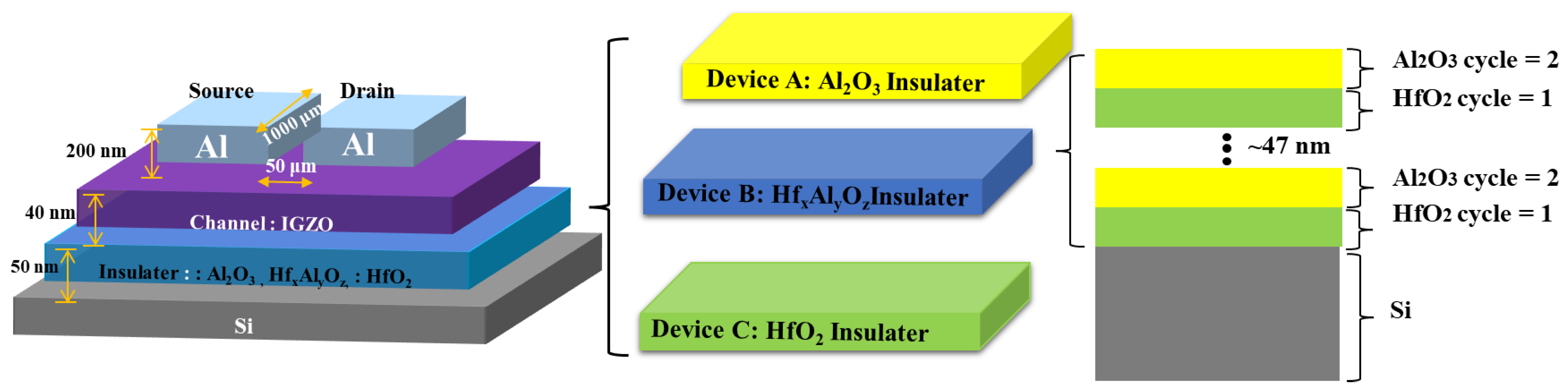
2. Experimental
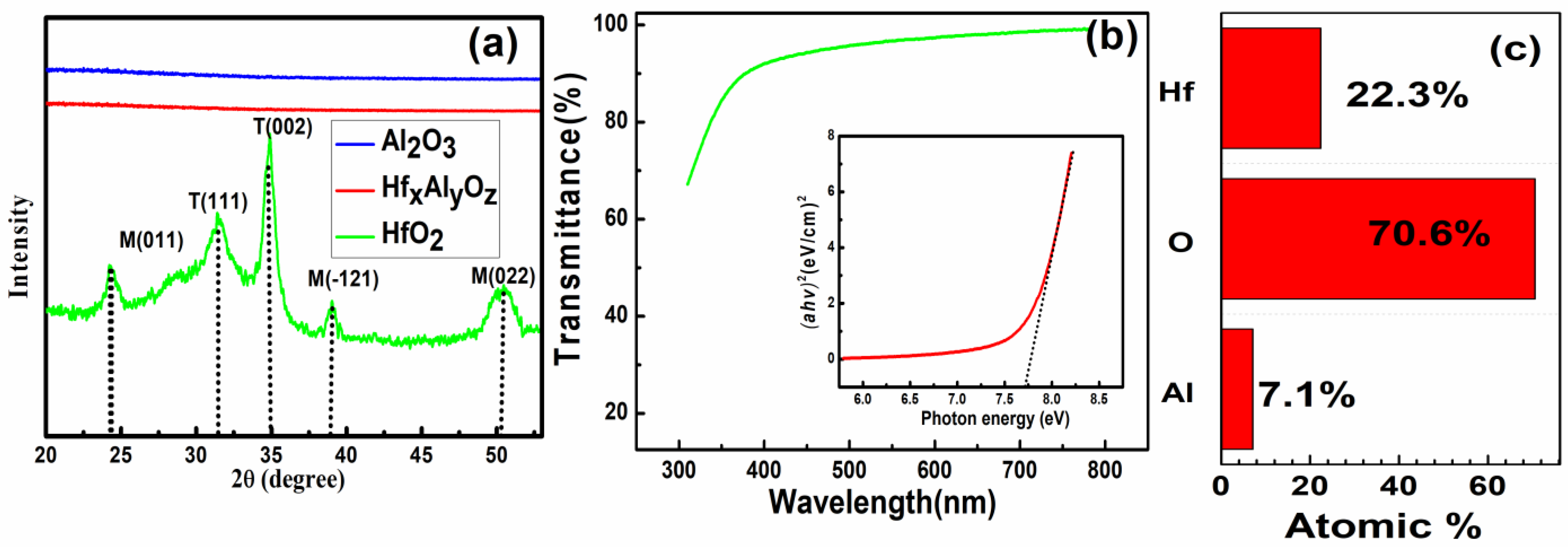
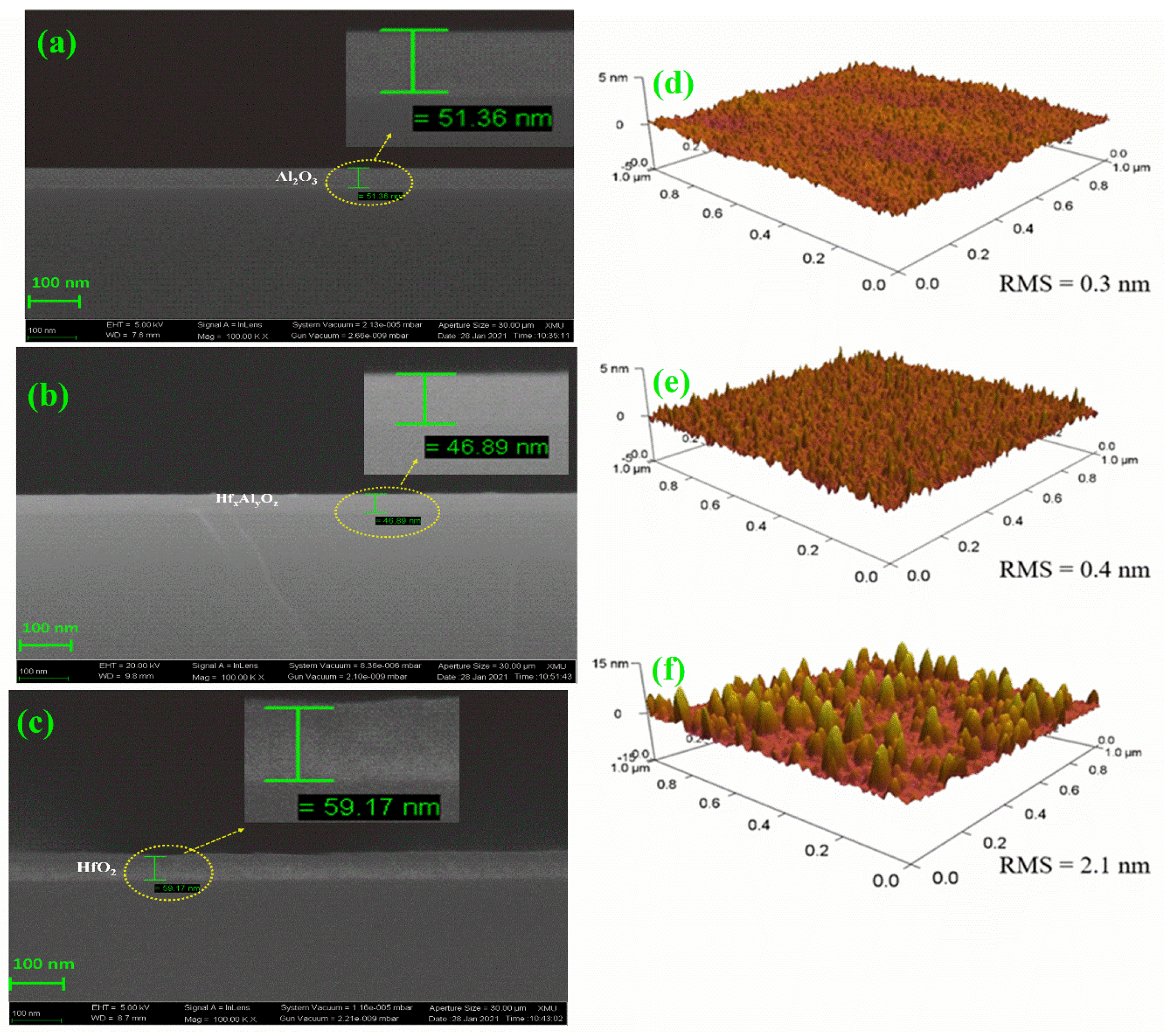
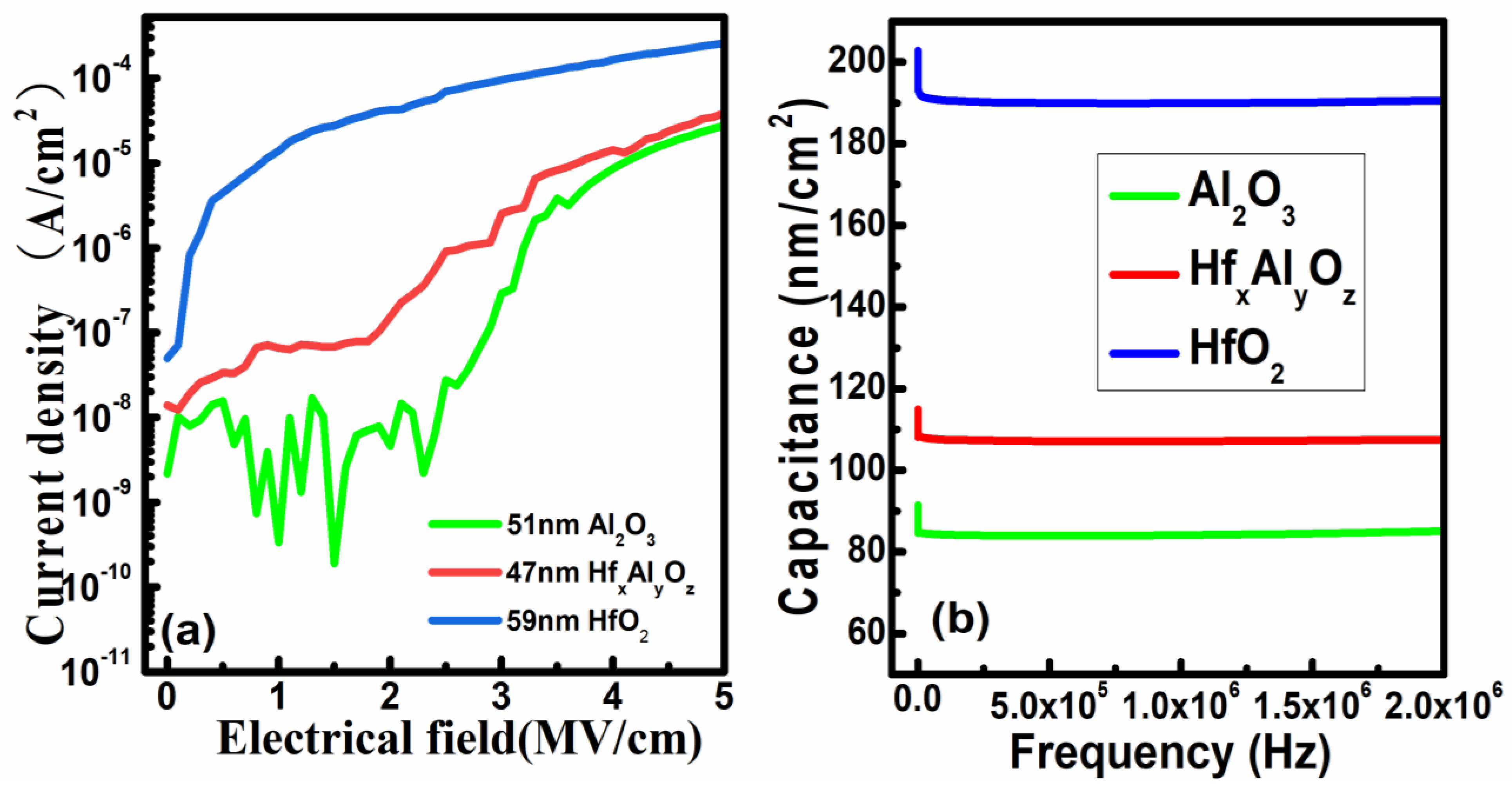
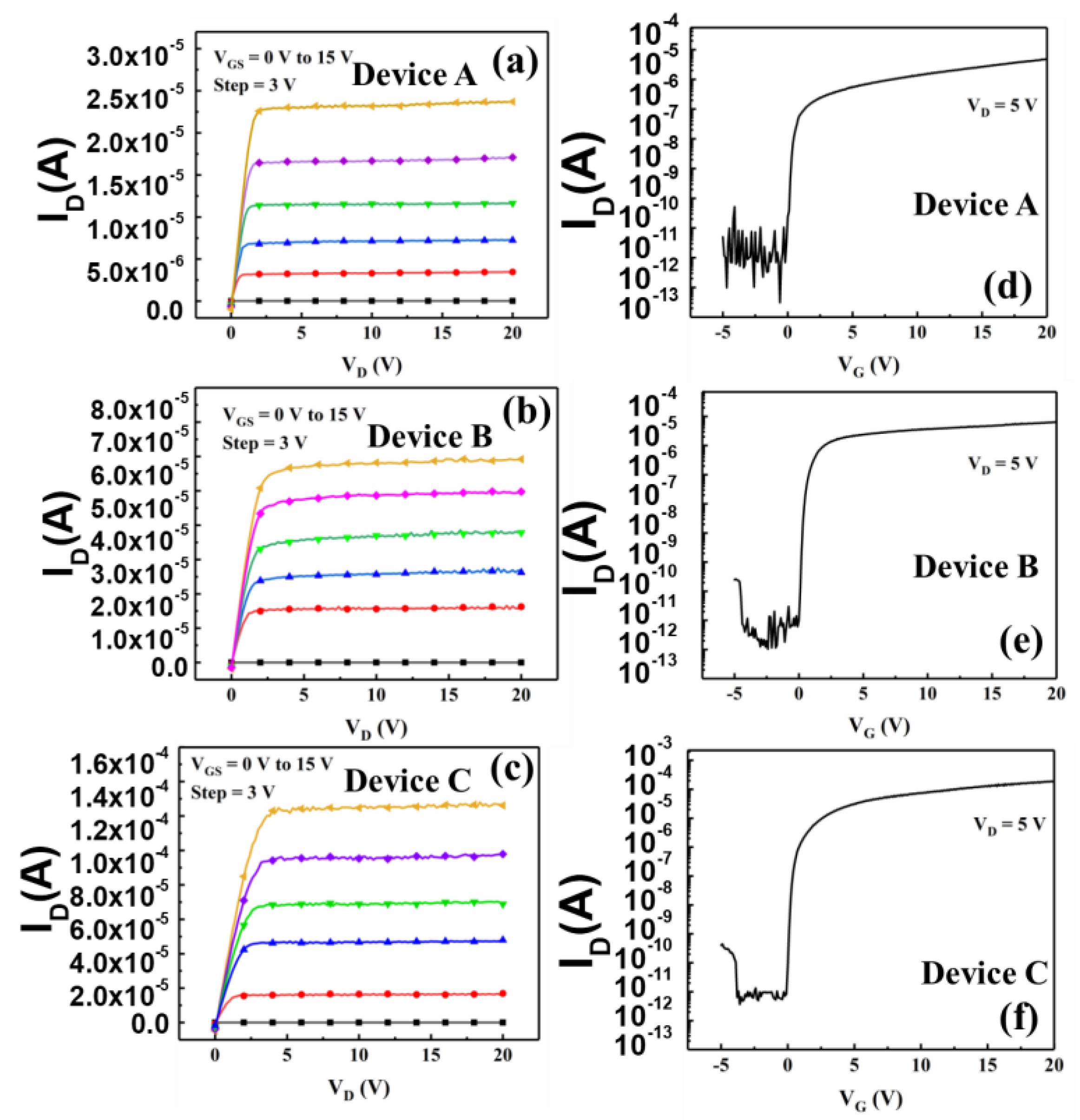
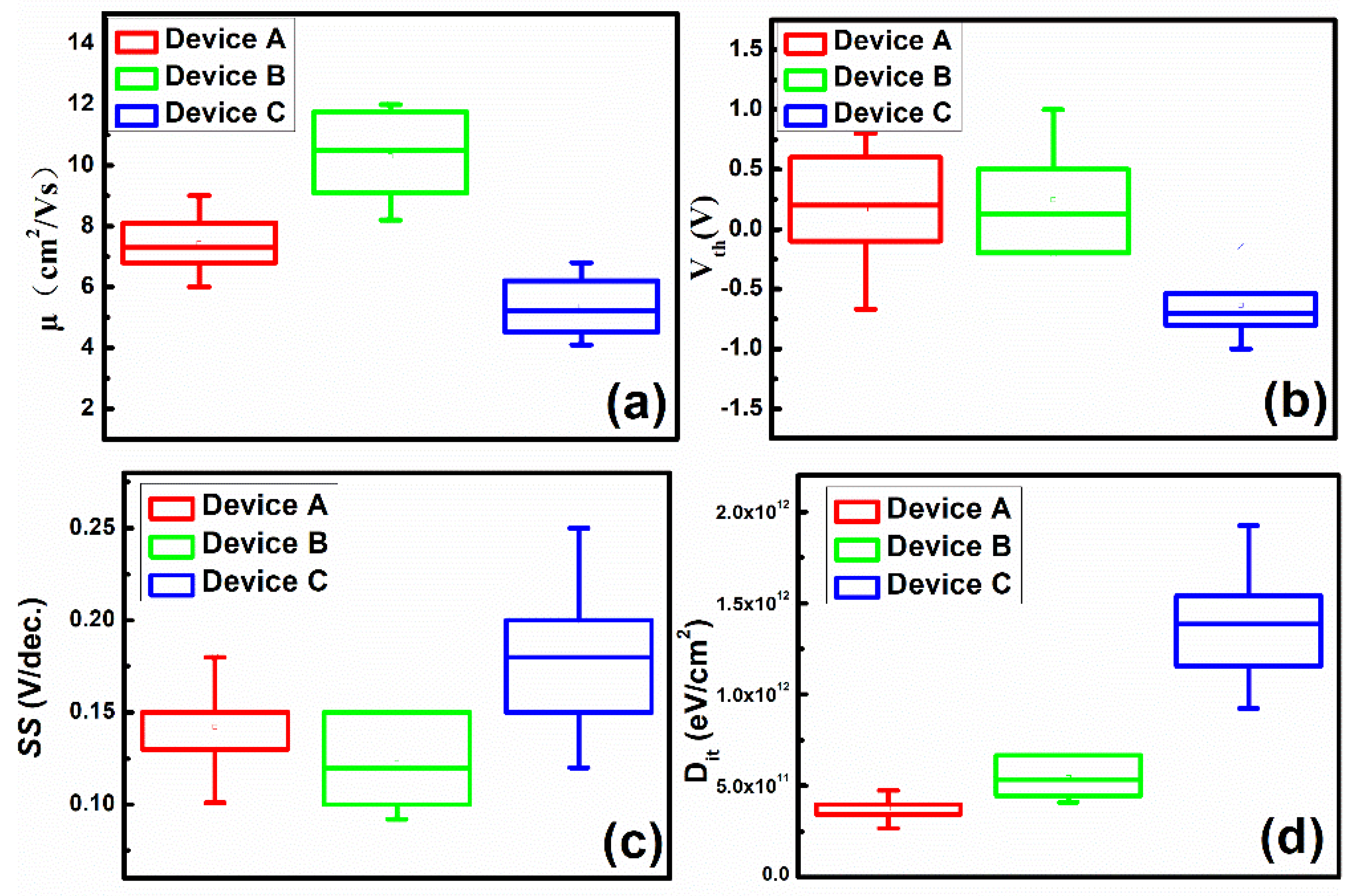
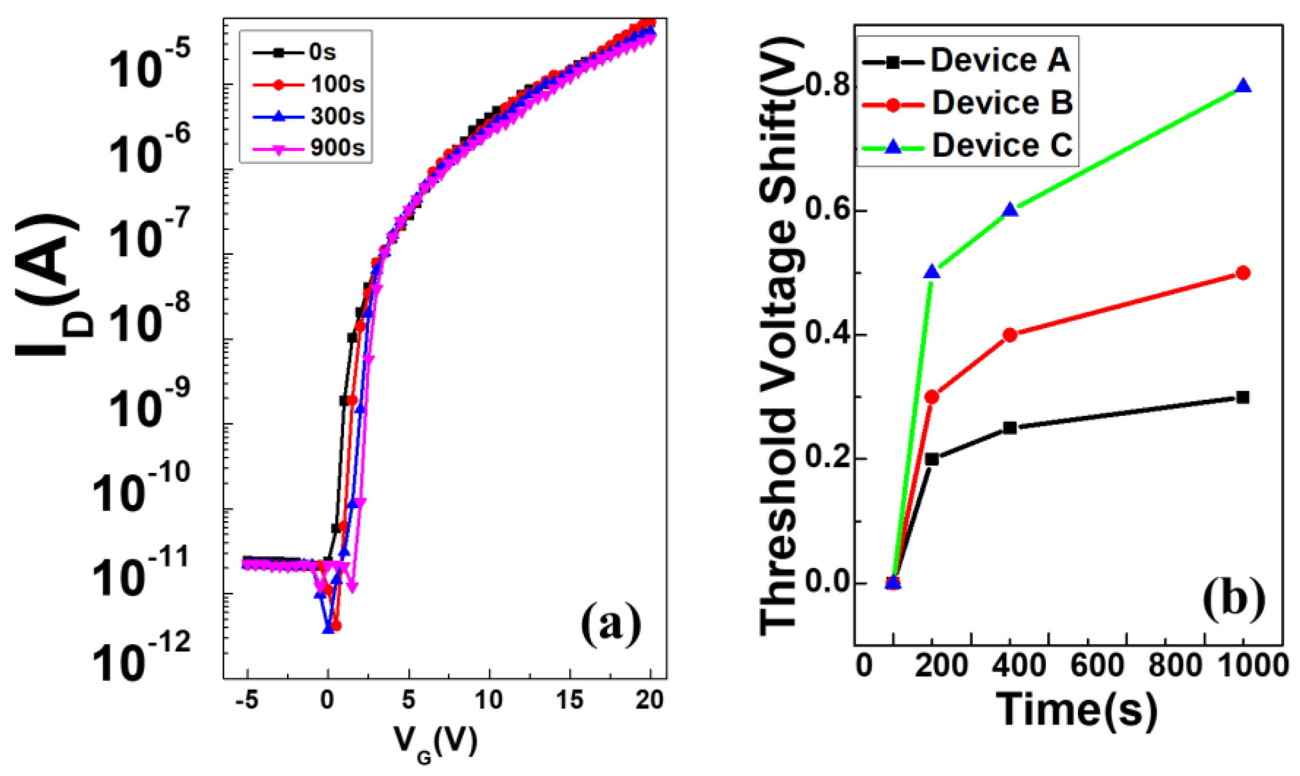
3. Results and Discussion
4. Conclusions
Author Contributions
Funding
Institutional Review Board Statement
Informed Consent Statement
Data Availability Statement
Conflicts of Interest
References
- Lin, D.; Su, W.; Chang, T.; Chen, H.; Tu, Y.; Zhou, K.; Hung, Y. Degradation Behavior of Etch-Stopper-Layer Structured a-InGaZnO Thin-Film Transistors Under Hot-Carrier Stress and Illumination. IEEE Trans. Electron Devices 2021, 68, 556–559. [Google Scholar] [CrossRef]
- Wang, C.; Zhu, H.; Meng, Y.; Nie, S.; Zhao, Y.; Shin, B.; Fortunato, E.; Martin, R. Sol–Gel Processed p-Type CuAlO 2 Semiconductor Thin Films and the Integration in Transistors. IEEE Trans. Electron Devices 2019, 66, 1458–1463. [Google Scholar] [CrossRef]
- Liu, A.; Zhu, H.; Guo, Z.; Meng, Y.; Liu, G.; Fortunato, E.; Martins, R.; Sha, F. Solution Combustion Synthesis: Low-Temperature Processing for p-Type Cu: NiO Thin Films for Transparent Electronics. Adv. Mater. 2017, 29, 1701599. [Google Scholar] [CrossRef] [PubMed]
- Nomura, K.; Ohta, H.; Takagi, A.; Kamiya, T.; Hirano, M.; Hosono, H. Room-temperature fabrication of transparent flexible thin-film transistors using amorphous oxide semiconductors. Nature 2004, 432, 488–492. [Google Scholar] [CrossRef] [PubMed]
- Ruan, D.; Liu, P.; Chien, T.; Chiu, Y.; Gan, K.; Sze, S.M. High Performance Transparent a-IGZO Thin Film Transistors with ALD-HfO2 Gate Insulator on Colorless Polyimide Substrate. IEEE Trans. Nanotechnol. 2020, 19, 481–485. [Google Scholar]
- Seul, H.J.; Kim, M.J.; Yang, H.J.; Cho, M.H.; Song, W.-B.; Jeong, J.K.; Cho, M.H. Atomic Layer Deposition Process-Enabled Carrier Mobility Boosting in Field-Effect Transistors through a Nanoscale ZnO/IGO Heterojunction. ACS Appl. Mater. Interfaces 2020, 12, 33887–33898. [Google Scholar] [CrossRef]
- Zhang, Y.; Zhang, H.; Che, B.; Yang, J.; Zhang, J.; Ding, X. A New “Ammonia Bath” Method for Realizing Nitrogen Doping in ZnSnO Transistors. IEEE Electron Device Lett. 2019, 41, 389–392. [Google Scholar] [CrossRef]
- Yang, J. High-Performance 1-V ZnO Thin-Film Transistors with Ultrathin, ALD-Processed ZrO2 Gate Dielectric. IEEE Trans. Electron Devices 2019, 66, 3382–3386. [Google Scholar] [CrossRef]
- Zhang, Y.; Zhang, H.; Yang, J.; Ding, X.; Zhang, J. Solution-Processed Yttrium-Doped IZTO Semiconductors for High-Stability Thin Film Transistor Applications. IEEE Trans. Electron. Devices 2019, 66, 5170–5176. [Google Scholar] [CrossRef]
- Islam, M.; Saha, J.K.; Bukke, R.N.; Hasan, M.; Billah, M.M.; Mude, N.N.; Ali, A.; Jang, J. Solution-Processed La Alloyed ZrOx High-k Dielectric for High-Performance ZnO Thin-Film Transistors. IEEE Electron. Device Lett. 2020, 41, 1021–1024. [Google Scholar] [CrossRef]
- Cheng, T.H.; Chang, S.P.; Cheng, Y.C. Indium Aluminum Zinc Oxide Phototransistor with HfO2 Dielectric Layer Through Atomic Layer Deposition. IEEE Sens. J. 2019, 20, 1838–1842. [Google Scholar] [CrossRef]
- Park, S.; Clark, B.L.; Keszler, D.A.; Bender, J.P.; Wager, J.F.; Reynolds, T.A.; Herman, G.S. Low-Temperature Thin-Film Deposition and Crystallization. Science 2002, 297, 65. [Google Scholar] [CrossRef] [PubMed] [Green Version]
- Lucovsky, G.; Fulton, C.C.; Zhang, Y.; Zou, Y.; Luning, J.; Edge, L.F.; Whitten, J.L.; Nemanich, R.J.; Ade, H.; Schlom, D.G.; et al. Conduction Band-Edge States Associated with the Removal of d-State Degeneracies by the Jahn–Teller Effect. IEEE Trans. Device Mater. Reliab. 2005, 5, 65–83. [Google Scholar] [CrossRef] [Green Version]
- Nomura, K.; Ohta, H.; Ueda, K.; Kamiya, T.; Hirano, M.; Hosono, H. Thin-Film Transistor Fabricated in Single-Crystalline Transparent Oxide Semiconductor. Science 2003, 300, 1269–1272. [Google Scholar] [CrossRef] [PubMed]
- Oh, M.S.; Hwang, D.; Lee, K.; Im, S.; Yi, S. Low voltage complementary thin-film transistor inverters with pentacene-ZnO hybrid channels on AlOx dielectric. Appl. Phys. Lett. 2007, 90, 173511. [Google Scholar] [CrossRef]
- Yim, K.; Yong, Y.; Lee, J.; Lee, K.; Nahm, H.-H.; Yoo, J.; Lee, C.; Hwang, C.S.; Han, S. Novel high-κ dielectrics for next-generation electronic devices screened by automated ab initio calculations. NPG Asia Mater. 2015, 7, e190. [Google Scholar] [CrossRef]
- Zhang, J.; Ding, X.; Li, J.; Zhang, H.; Jiang, X.; Zhang, Z. Performance enhancement in InZnO thin-film transistors with compounded ZrO2–Al2O3 nanolaminate as gate insulators. Ceram. Int. 2016, 42, 8115–8119. [Google Scholar] [CrossRef]
- Zhou, X.; Yang, H.; Chang, B.; Liang, T.; Wang, Y.; Zhang, S. Homo-Junction Bottom-Gate Amorphous In–Ga–Zn–O TFTs with Metal-Induced Source/Drain Regions. IEEE J. Electron Devices Soc. 2019, 7, 52–56. [Google Scholar]
- Li, H.; Han, D.; Dong, J.; Yu, W.; Liang, Y.; Luo, Z.; Zhang, S.; Zhang, X.; Wang, Y. Enhanced electrical properties of dual-layer channel ZnO thin film transistors prepared by atomic layer deposition. Appl. Surf. Sci. 2018, 439, 632–637. [Google Scholar] [CrossRef]
- Souri, D.; Tahan, Z.E. A new method for the determination of optical band gap and thenature of optical transitions in semiconductors. Appl. Phys. B 2015, 119, 273–279. [Google Scholar] [CrossRef]
- Costa, J.C.; Taveira, R.J.; Lima, C.F.; Mendes, A.; Santos, L.M. Optical band gaps of organic semiconductor materials. Opt. Mater. 2016, 58, 51–60. [Google Scholar] [CrossRef]
- Dolgonos, A.; Mason, T.O.; Poeppelmeier, K.R. Direct optical band gap measurement in polycrystalline semiconductors: A critical look at the Tauc method. J. Solid State Chem. 2016, 240, 43–48. [Google Scholar] [CrossRef]
- Liu, L.-C.; Chen, J.-S.; Jeng, J.-S. Role of oxygen vacancies on the bias illumination stress stability of solution-processed zinc tin oxide thin film transistors. Appl. Phys. Lett. 2014, 105, 023509. [Google Scholar] [CrossRef]


Publisher’s Note: MDPI stays neutral with regard to jurisdictional claims in published maps and institutional affiliations. |
© 2022 by the authors. Licensee MDPI, Basel, Switzerland. This article is an open access article distributed under the terms and conditions of the Creative Commons Attribution (CC BY) license (https://creativecommons.org/licenses/by/4.0/).
Share and Cite
Huang, C.; Liu, Y.; Ma, D.; Guo, Z.; Yao, H.; Lv, K.; Tian, Z.; Liang, L.; Gao, J.; Ding, X. High Performance of InGaZnO TFTs Using HfxAlyOz Nanolaminates as Gate Insulators Prepared by ALD. Coatings 2022, 12, 1811. https://doi.org/10.3390/coatings12121811
Huang C, Liu Y, Ma D, Guo Z, Yao H, Lv K, Tian Z, Liang L, Gao J, Ding X. High Performance of InGaZnO TFTs Using HfxAlyOz Nanolaminates as Gate Insulators Prepared by ALD. Coatings. 2022; 12(12):1811. https://doi.org/10.3390/coatings12121811
Chicago/Turabian StyleHuang, Chuanxin, Yunyun Liu, Dianguo Ma, Zhongkai Guo, Haiyun Yao, Kaikai Lv, Zhongjun Tian, Lanju Liang, Ju Gao, and Xingwei Ding. 2022. "High Performance of InGaZnO TFTs Using HfxAlyOz Nanolaminates as Gate Insulators Prepared by ALD" Coatings 12, no. 12: 1811. https://doi.org/10.3390/coatings12121811