Article

Synthesis of High Quality Transparent Nanocrystalline Diamond Films on Glass Substrates Using a Distributed Antenna Array Microwave System

Laboratoire des Sciences des Procédés et des Matériaux, Université Sorbonne Paris Nord, CNRS, UPR 3407, F-93430 Villetaneuse, France
*
Author to whom correspondence should be addressed.
Coatings 2022, 12(10), 1375; https://doi.org/10.3390/coatings12101375
Submission received: 5 August 2022 / Revised: 16 September 2022 / Accepted: 16 September 2022 / Published: 20 September 2022
(This article belongs to the Collection Feature Paper Collection in Thin Films)

Abstract

:
Diamond is a material of choice for the fabrication of optical windows and for protective and anti-reflecting coatings for optical materials. For these kinds of applications, the diamond coating must have a high purity and a low surface roughness to guarantee a high transparency. It should also be synthesized at low surface temperature to allow the deposition on low melting-point substrates such as glasses. In this work, the ability of a Distributed Antenna Array (DAA) microwave system operating at low temperature and low pressure in H2/CH4/CO2 gas mixture to synthesize nanocrystalline diamond (NCD) films on borosilicate and soda-lime glass substrates is investigated aiming at optical applications. The influence of the substrate temperature and deposition time on the film microstructure and optical properties is examined. The best film properties are obtained for a substrate temperature below 300 °C. In these conditions, the growth rate is around 50 nm·h−1 and the films are homogeneous and formed of spherical aggregates composed of nanocrystalline diamond grains of 12 nm in size. The resulting surface roughness is then very low, typically below 10 nm, and the diamond fraction is higher than 80%. This leads to a high transmittance of the NCD/glass systems, above 75%, and to a low absorption coefficient of the NCD film below 103 cm−1 in the visible range. The resulting optical band gap is estimated at 3.55 eV. The wettability of the surface evolves from a hydrophilic regime on the bare glass substrates to a more hydrophobic regime after NCD deposition, as assessed by the increase of the measured contact angle from less than 55° to 76° after the deposition of 100 nm thick NCD film. This study emphasizes that such transparent diamond films deposited at low surface temperature on glass substrate using the DAA microwave technology can find applications for optical devices.

Graphical Abstract

1. Introduction

Diamond is an unsurpassed champion among materials due to its outstanding and unmatched properties, such as high thermal conductivity, excellent hardness, high transparency in a large spectral range, biocompatibility and electronic properties. These properties make it an extremely attractive candidate for electronic, thermal, mechanical, biomedical and optical applications [1].
In the optical field, the use of diamond films is regarded as one of most promising applications of the Chemical Vapor Deposition (CVD) diamond technology. For example, polycrystalline diamond windows have been manufactured for high power CO2 lasers [2]. It is also a material of choice for optical windows [3,4] and protective coatings for optical materials such as optical fibres [5]. Anti-reflecting and protective coatings for solar cells [6] can be also expected.
Diamond films with high sp3 content are required to ensure high transparency since the presence of sp2 non-diamond absorbent phases reduces the transmission of the diamond films, limiting their use in optical coatings [7]. Moreover, a low surface roughness of these diamond films is needed in order to avoid scattering events and attenuation, which cannot be ignored if the surface roughness is comparable to the wavelength of the light source [8].
In contrast to rough polycrystalline diamond films, for which a polishing process is necessary to reach the surface smoothness needed for most of optical applications, nanocrystalline diamond (NCD) films have the advantage of providing an as-grown smooth surface that does not require a time-consuming post-deposition polishing process owing to a very small grain size (5–20 nm) [9,10] which is independent of the film thickness [11]. Moreover, these films can be deposited at low temperatures, which permits the deposition on low-melting-point substrates such as various types of glasses [12]. However, the presence of non-diamond phases, more specifically graphitic sp2 phases, in the NCD films can drastically affect their optical characteristics by causing absorption. For instance, it has been found that the non-diamond sp2 phases in NCD films are responsible for an onset of optical absorption around 0.8 eV [13]. The NCD growth process must then ensure a nanometric grain size, a satisfactory growth rate and a high purity to fulfil the requirements for optical applications.
The synthesis of NCD films is typically performed using hot filament (HF CVD) [14,15] or microwave plasma assisted chemical vapor deposition (MPACVD) [10]. The HFCVD is commercially more interesting as it is inexpensive and allows the deposition of diamond on large surfaces and complex geometry substrates. However, with the filament placed very close to the substrate, long-term filament degradation leads to strong contamination of the deposited diamond films, as well as inhomogeneity of the temperature distribution along the filament [16]. Resonant-cavity MWPECVD systems, mainly operating at 2.45 GHz frequency, can be used to deposit high purity diamond films, but at a disadvantage of deposition area. The size of the plasma in this type of reactor is indeed limited by the microwave frequency (typically 2 inches at 2.45 GHz) [17]. The deposition area can be increased in resonant-cavity MPACVD by using a lower frequency (915 MHz) and increasing the input microwave power, which leads to higher capital cost [18]. The deposition of diamond with both HFCVD and MPACVD methods is carried out at high temperatures (600–1000 °C) which prevent diamond films deposition on temperature sensitive substrates [19], in particular glass substrates.
In order to overcome the drawbacks mentioned above, distributed antenna array (DAA) [20,21], surface wave [22] and linear antenna [23] systems have been developed as promising alternatives to HFCVD and MPACVD reactors operating in resonant cavities. Working in H2/CH4/CO2 gas mixture, they allow NCD films deposition at lower substrate temperatures (<400 °C) and on large areas (>600 cm2).
The plasma in linear antenna reactors is excited by a set of coaxial linear antennas, each surrounded by a quartz tube [24], fed by low, medium, or high microwave power, up to 20 kW, using microwave generators operating in continuous or pulsed mode [25]. This kind of system enables NCD film deposition on large areas with high plasma density (1011 cm−3) and low electron temperature (1.5 eV) [26]. However, for temperature-sensitive substrates coating, such as glass substrates, it is necessary to use a water-cooled substrate holder in order to control the substrate temperature. It is also worth noting that the coaxial linear antenna system suffers from the formation of a standing electromagnetic wave along each antenna which leads to a non-uniform plasma distribution, thereby affecting the homogeneity of deposition process over the substrate [27]. On the other hand, the DAA plasma enhanced system is composed of a set of elementary sources arranged in a two-dimensional matrix configuration. The plasma in this reactor can reach high electron densities up 1013 cm−3 with uniformity better than ±3.5% [28] and growth rates up to 100 nm·h−1 [20] by working at only a few kW microwave power. Low temperature NCD films growth with DAA reactors was demonstrated down to 250 °C on silicon and silicon nitride and other temperature-sensitive substrates [20,21]. It has been also demonstrated that this type of reactor makes it possible to achieve very homogeneous diamond films deposition on 3D and complex-shape substrates at low temperatures, while maintaining the same planar configuration of the sources, without fundamentally modifying the reactor design [29].
In the present study we investigate the deposition of NCD films grown for the first time on borosilicate and soda-lime glass slides using a distributed antenna array (DAA) microwave reactor composed of 16 coaxial microwave plasma sources, arranged in a 2D matrix and yielding a very large plasma size (>600 cm2), at low substrate temperatures (≤400 °C), using H2/CH4/CO2 gas mixture at low pressure (<1 mbar). The influence of substrate temperature and deposition time on the microstructure, as well as optical properties and wettability of the grown NCD films have been investigated.

2. Materials and Methods

NCD films were grown on glass substrates using a DAA microwave reactor, the details of which can be found elsewhere [20,30], with the following process conditions: gas mixture 96.4% H2, 2.6% CH4 and 1% CO2 with 50 sccm total flow rate, an operating pressure of 0.35 mbar and a microwave power of 3 kW. Substrates were directly placed on a molybdenum holder equipped with a graphite heater, and the substrate temperature was regulated by a thermocouple embedded in the substrate holder. The substrate holder is localized at 10 cm from the plasma sources. The growth parameters described above correspond to those usually employed for the deposition of NCD films on silicon substrates which give a good compromise between thickness homogeneity, growth rate and microstructure [30]. Two series of samples were achieved. For series B, the substrate was a borosilicate glass of 250 µm thickness. The substrate temperature was maintained at 300 °C during the growth, and the deposition time was varied between 2 and 4 h. For series S, the substrate was a soda-lime glass of 1 mm thickness. The deposition time was set at 2 h, whereas the substrate temperature was varied between 265 °C and 400 °C. Table 1 summarizes the growth conditions for both sample series. Prior to plasma treatment, the substrates were seeded by spin coating using a colloidal solution containing 25 nm grain size diamond powder (SYP-GAF-0-0.05 provided by Van Moppes) diluted in water, and polyvinyl alcohol (PVA) powder was added in order to avoid coagulation.
The NCD film thickness was determined ex situ by using a UV–visible reflectometer (NanoCalc, Ocean optics, Dunedin, FL, USA), which was also employed for estimating the reflectance of the samples.
The film morphology was investigated by top-view scanning electron microscopy (SEM) taken by a field emission ZEISS ULTRA plus system (Carl Zeiss, Jena, Germany) operating at 3 kV. A thin (5 nm) additional conductive layer was deposited on the sample before characterization to avoid any charge effects.
The surface topography was analyzed with a Brucker ICON Dimension Atomic Force Microscopy (AFM) (Bruker, Billerica, MA, USA) system working in tapping mode in air.
Raman spectra were obtained with a HR800 (HORIBA Jobyn-Yvon, Edison, NJ, USA) apparatus operating at 473 nm excitation wavelength allowing the examination of the phase purity of the deposited films. The purity of the deposited films was roughly estimated from deconvoluted Raman spectra using LabSpec version 5 software through the sp3 fraction defined as:
sp 3 % = 100 · 60 · I d i a m o n d 60 · I d i a m o n d + I n o n d i a m o n d
where Idiamond is the Raman diamond peak area at 1332 cm−1, which represents sp3 phase, and I n o n   d i a m o n d is the sum of Raman non-diamond peak areas. A Raman signal efficiency factor averaged ratio of 60 between non-diamond and sp3 phases was estimated for the considered excitation wavelength of 473 nm according to the works of Klauser et al. carried out for different wavelengths [31,32].
The surface wettability was estimated from the water contact angles, which were measured under ambient conditions both on the glass substrates before deposition and on the NCD films using a drop shape analyzer DSA25 from KRÜSS. The contact angle of dH2O (2 μL) on the surface was recorded 10 s after contact and at least 3 measurements were taken and averaged.
The microstructure and grain size of the NCD films were assessed through X-ray diffraction (XRD) patterns (INEL Equinoxe 1000) obtained using the CuKα1 radiation (λ = 1.54056 Å) with an incident X-ray angle of 2°. The grain size was estimated using a modified Scherrer equation applied on the diamond diffraction peaks [33]:
ln β = ln K λ L + ln 1 cos θ
with β the FWHM of the diffraction peak, λ the wavelength of the X-ray source, θ the half of the Bragg’s angle, K a constant which depends on the crystallites shape and L the crystallites size.
The transmittance of the samples before and after deposition was measured using a UV–visible Avaspec-2048 × 14 spectrometer from Avantes.
The experimental determination of optical properties of the NCD films, such as absorption coefficient and optical band gap, involves the measurement of the transmittance and reflectance of the NCD layer itself, i.e., measured on a free-standing film, which is not possible in the case of very thin films such as those investigated here. However, the transmittance and reflectance of the single film (Tf, Rf) under normal observation can be calculated knowing the transmittance and reflectance of the substrate (Tsub, Rsub) and of the film/substrate system (Tsys, Rsys) using the following equations [34]:
T f λ = T s y s T s u b 1 R s y s R s u b T s u b 2 T s y s 2 R s u b 2
R f λ = R s y s T s u b 2 T s y s 2 R s u b T s u b 2 T s y s 2 R s u b 2
In order to calculate the absorption coefficient α , it is still necessary to determine the so-called “reflection coefficient” R that can be derived along with α from equations 5 and 6 using an iterative method as described in [35]:
R = R f R 1 R 2 e 2 α d 1 R 2 e 2 α d
e α d = 1 R A f 1 R R A f
where d is the NCD film thickness and A f = 1 R f T f is the absorbance of the film. These equations are correct for NCD films with nanometric grains size and surface roughness, as those studied here, for which the scattering at the interfaces and at the grain boundaries can be neglected. The corresponding optical band gap of the film was calculated using the Tauc’s model [36]. In this method, the absorption spectrum of the sample is fitted with power law function, given by the Tauc’s equation for indirect allowed band distribution [37,38]:
α h ν = B h ν E g 2
where h is the Planck’s constant, ν is the frequency of radiation, E g is the optical band gap and B is the slop of the straight line extrapolated on the energy axis. The optical band gap E g can be determined from the plot of α h ν 1 2 vs. photon energy E = h ν as the intercept of the extrapolated linear fit with the abscissa axis.

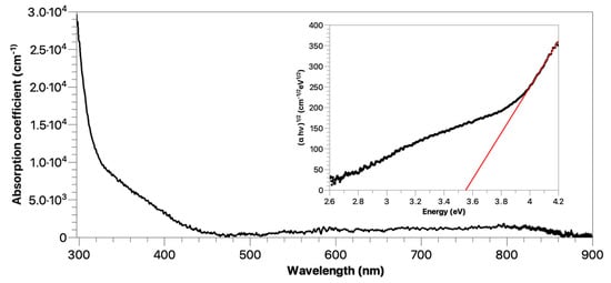
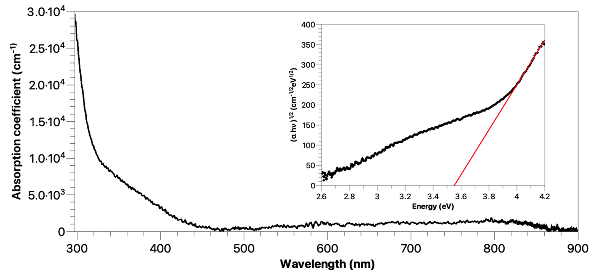
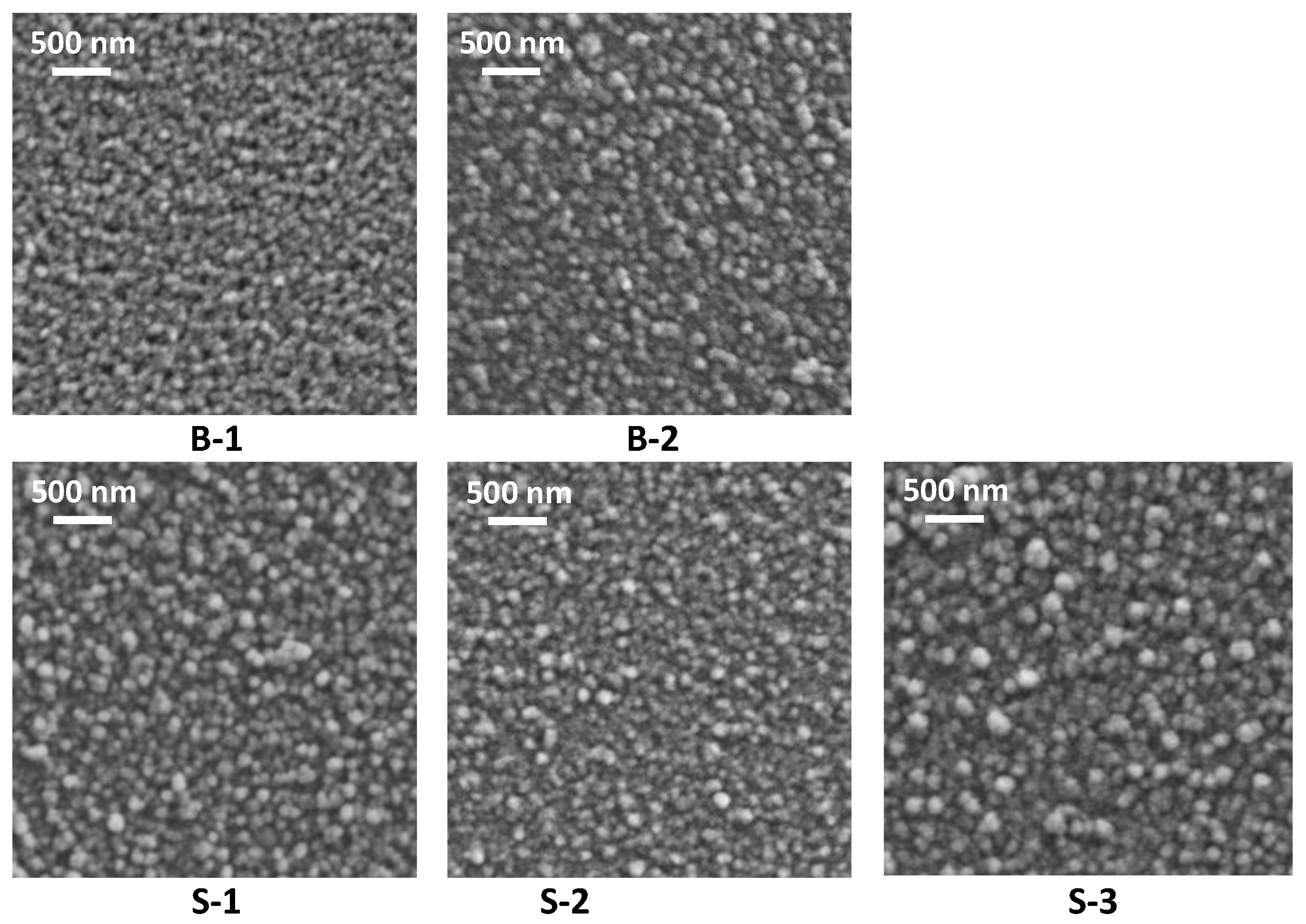
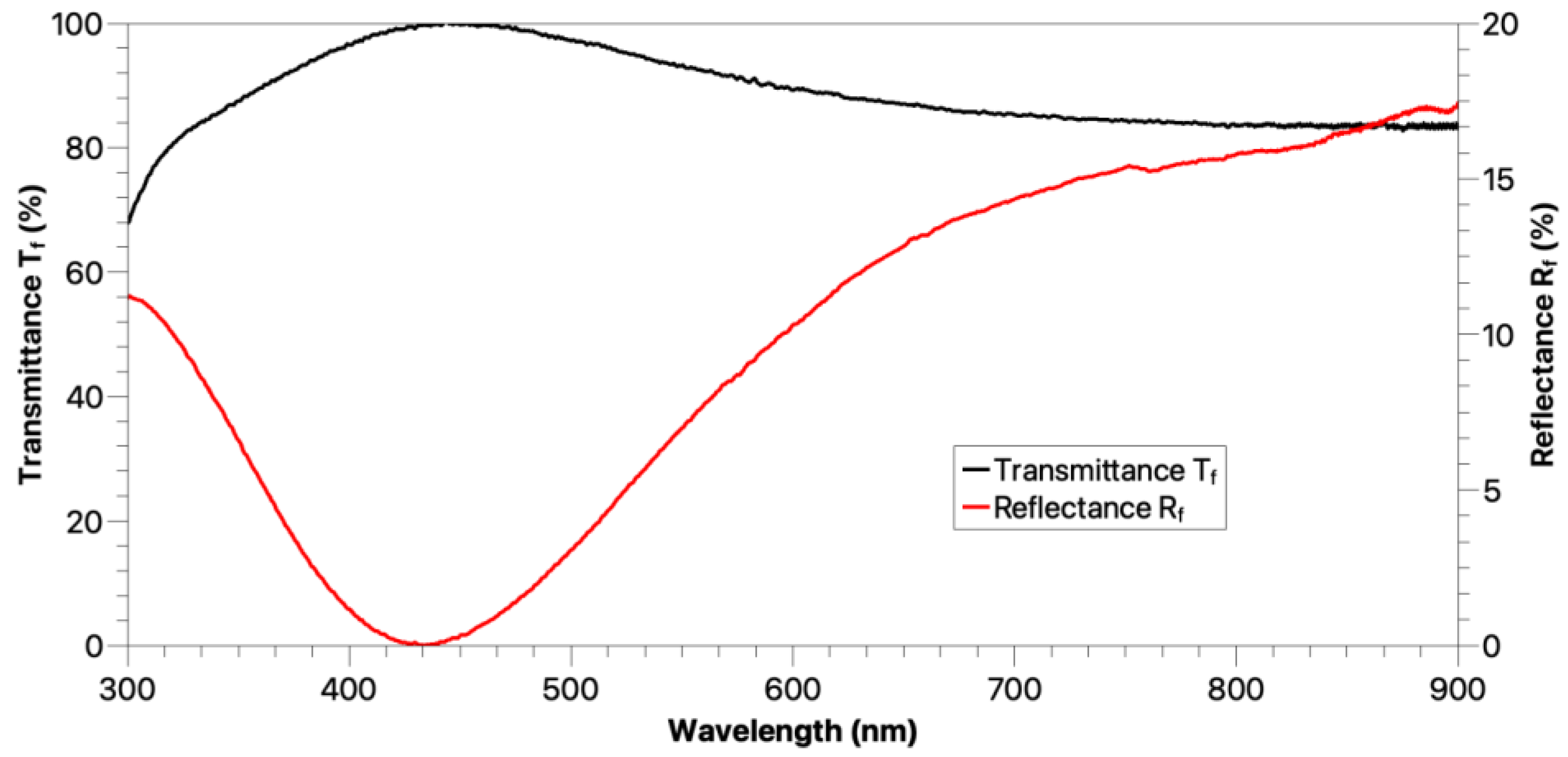
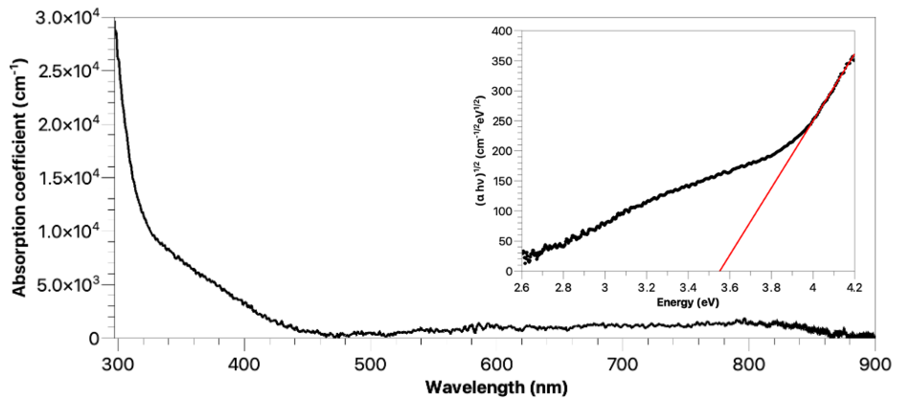
3. Results and Discussion

The NCD film thickness and the resulting growth rate are given in Table 1. The thickness of the samples of series B grown at 300 °C increases with the deposition time from 96 nm for 2 h to 153 nm for 4 h, which corresponds to a growth rate of 48 nm·h−1 and 38.3 nm·h−1, respectively. Since the accurateness of the thickness measurement was estimated at ±10%, the growth rate remains roughly constant as a function of the deposition time. Samples of series S grown during 2 h have a growth rate, and, therefore, a film thickness, which increase when the substrate temperature varies from 265 to 400 °C. This behavior is comparable to the one reported for the DAA microwave system when using conventional substrates such as silicon in similar growth conditions [39]. The growth rate thus increases from 39.5 nm·h−1 to 55 nm·h−1 leading to a thickness variation from 79 to 110 nm. For both sample series, the films elaborated at 300 °C during 2 h (samples B-1 and S-2) exhibit a similar growth rate around 50 nm·h−1, which shows that the nature and thickness of the glass substrate do not influence the nucleation process and the growth kinetics. The values of the growth rates reported in Table 1 are also consistent with previous studies carried out with a DAA microwave system when using silicon substrate [30,31].
The morphology of the deposited films assessed by SEM (Figure 1) reveals that the surface is homogeneously covered by nanometric spherulitic aggregates. This is characteristic of NCD layers synthesized at low substrate temperature using a DAA microwave system in H2/CH4/CO2 gas mixture and results from a predominant high-rate secondary nucleation growth mode [30,31]. No significant difference is observed for both sample series as a function of the deposition time or substrate temperature.
The sample topography was investigated by AFM on small areas of 1 × 1 μm2 in order to examine the short-scale roughness resulting from aggregates of submicrometric size. The AFM micrographs obtained on the thickest film (Sample B-2) are given in Figure 2 as an illustrative example. The AFM micrographs are consistent with the SEM observations since unfaceted aggregates of size between a few tens and a few hundred nanometers are evidenced at the film surface. The resulting surface root mean square (Rms) roughness measured from the AFM micrographs for the samples of series B and S are given in Table 1. Whatever the growth conditions, the Rms roughness values are in the range 4.9–10.5 nm, which points out, taking the precision of measurement into account, that the substrate’s nature and thickness, the substrate temperature and the film thickness have a very limited effect on the surface topography after deposition. In comparison the Rms roughness of the glass bare substrates is 2 nm (Samples B-0 and S-0). It should be noticed that the no prominent effect of the substrate temperature on the film topography cannot be explained by the small thickness of the films, since for similar thicknesses a significant effect of the pressure and the substrate position on the NCD films topography has been observed by Baudrillart et al. [30]. The aggregate size and, consequently, the surface roughness of NCD films elaborated on glass substrate in the considered growth condition in the DAA reactor are thus independent of the deposited thickness. These very low values of the Rms roughness are particularly well adapted for optical applications, for example transparent protective coatings, when using wavelengths in ultraviolet, visible or near infrared ranges. Indeed, the film interfaces can be considered planar from an optical point of view and the light scattering due to diamond aggregates would be negligible.
Raman spectra of the samples of both series are shown in Figure 3. For all the samples, a weak and broad diamond peak at 1332 cm−1 is well visible along with broad bands centered around 1350 cm−1 and 1580 cm−1, which correspond to graphite D and G bands, respectively [40]. Trans-polyacetylene (TPA) responses at around 1140 cm−1 (C-H in plane bending) and 1480 cm−1 (C=C stretch) are also noticed on all the spectra and are the fingerprint of nanocrystalline diamond [41,42,43]. The diamond films deposited on glass substrates with the DAA microwave system thus exhibit a nanocrystalline feature. Figure 4 shows an example of Raman spectrum deconvolution for sample S-2 taking 8 contributions into account, including diamond peak, TPA bands and graphite bands. The Full Width at Half Maximum (FWHM) of the diamond peak reached from Raman spectra deconvolution is reported in Table 1 for all the samples. For the experimental conditions explored through both sample series, the FWHM is roughly constant and remains in the range 16.8–17.8 cm−1. These values are typical of a nanometric grain size [39] and are comparable to the values usually obtained on silicon substrates [31,44]. Besides, the quasi-constancy of the FWHM shows that the substrate nature, film thickness and substrate temperature do not influence significantly the NCD grain size for the experimental conditions considered here. The diamond content sp3 phase calculated using equation 1 is given in Table 1 for all the samples. For sample series B, the sp3 fraction remains roughly constant whatever the film thickness with values of 79% for sample B-1 and 82% for sample B-2. For sample series S, the sp3 fraction decreases from 84% (sample S-1, 265 °C) to 59% (sample S-3, 400 °C) when the substrate temperature is increased. Nevertheless, it must be emphasized that the value of the sp3 fraction in the range 79%–84% obtained at low temperature for both series is very satisfactory and comparable to the one obtained on the silicon substrate in optimized conditions [31].
In order to further investigate the NCD film microstructure, XRD was carried out on the thickest film (sample B-2). The XRD pattern thus obtained is given in Figure 5. Even if the diamond diffraction peaks are shadowed by the substrate contribution, especially the broad diffraction peak around 2θ = 24°, which is related to the amorphous nature of silica [45], the (111), (220) and (311) diamond reflection peaks, occurring at 2θ = 43.9°, 2θ = 75.3° and 2θ = 91.5°, respectively, are clearly visible. This is further evidence for the presence of crystalline diamond within the films. Taking the three diffraction peaks of diamond into account and using equation 2, the grain size was estimated around 12 ± 3 nm, which is characteristic of the nanocrystalline structure and comparable to the grain size obtained on silicon or other substrates such as silicon nitride or piezoelectric materials using a DAA microwave system in the considered experimental conditions [21,30,31,46]. As previously reported, the submicrometric aggregates observed at the film surface are then nano-structure ballas-like particles formed of nanometric diamond grains [30,39,47]. It should be noticed that the grain size estimated for sample B-2 is representative of the grain size for all the samples considered in this study since the FWHM of the Raman diamond peak is almost constant for all the experimental parameters investigated.
The transmittance measured between 250 and 900 nm through the glass substrates and the NCD/glass systems for sample series B and sample series S with a precision of ±2% is shown in Figure 6a,b, respectively. As expected, both glass substrates (samples B-0 and S-0) exhibit a strong absorption in the UV domain and a high increasing transmittance, above 87%, from 400 nm. The transmittance of all the samples covered by NCD layers presents oscillations that depend on the film thickness due to multiple reflections at the film interfaces. The transmittance values are higher than 75% from 400 nm for all the samples, except for sample S-3 (>70%), which is in good agreement with the sp3 fraction discussed previously. These transmittance values are comparable to those reported for NCD films deposited on glass substrate at low temperature [48,49,50]. That points out that the NCD films elaborated with the DAA microwave system are optically transparent in a broad spectral range.
The transmittance and reflectance of the borosilicate glass substrate (sample B-0) and of the NCD/glass system (sample B-1, which represents the best compromise between the deposition temperature and deposition time in terms of thickness (growth rate), roughness and sp3 content), were measured (Figure 7) in order to reach the NCD film transmittance Tf and reflectance Rf deduced from equations 3 and 4 (Figure 8). The absorption coefficient α calculated for sample B-1 using equations 5 and 6 is reported in Figure 9. It decreases from 3 × 104 cm−1 at 300 nm to less than 103 cm−1 from 480 nm up to 900 nm. These values of the absorption coefficient are consistent with those reported in other works for undoped NCD films elaborated by microwave process [51] but are also much lower than other works for doped or undoped NCD films [13,52], which demonstrates the high quality/high transparency of the NCD films elaborated using the DAA microwave system.
The optical band gap for sample B-1 was thus estimated at 3.55 ± 0.35 eV. This is a pretty high value compared to results reported in other works for NCD films. Indeed, Ralchenko et al. found values of the optical band gap between 2.2 and 0.2 eV for ultra-NCD synthesized by MPACVD process using Ar/H2/CH4 gas mixture when the N2 concentration in the feed gas increases from 0% to 25% [53]. Wang et al. reported Eg values decreasing from 4.3 to 3.2 eV when increasing the carbon concentration from 2% to 3% for NCD films deposited by Hot Filament CVD process in H2/CH4 gas mixture [54]. Therefore, the optical band gap of NCD films synthesized on glass substrate at low temperature with the DAA microwave system points out the satisfactory purity and the resulting transparency on a wide wavelength range of the deposited material, which may be then used as protective and/or functionalized transparent coating.
In order to assess the ability of such transparent NCD films to modify the glass surface properties, the wettability of the samples before and after deposition was investigated through contact angle measurements. Prior to the characterization, all samples were exposed to air after deposition. Results are reported in Table 1 for both glass substrates (samples B-0 and S-0) and for NCD films elaborated at 300 °C during 2 h (samples B-1 and S-2). The wettability of the surface is drastically modified by the diamond deposition since the contact angle increases from 54.3° and 40.5° for bare substrates B-0 and S-0, respectively, to around 76° after the deposition of almost 100 nm thick NCD film. This indicates that the as-grown NCD coated glass substrates are more hydrophobic than the bare glass substrates. Such a property could be further enhanced through suitable plasma post-treatments to obtain, for example, fluorine or hydrogen termination [55]. Especially, in the case of the film hydrogenation, the increase of the hydrophobic properties has been attributed to a reduction in a polar component of the surface energy due to hydrogen adsorption-induced reconstruction of the film surface [56]. In the present case, the improvement of the hydrophobic behavior can be due to an efficient H-termination resulting from the significant H-atom density yielded in the synthesis discharge [39]. It should also be noticed that the surface wettability depends strongly, among others, on the surface roughness, film microstructure or exposure time to the atmosphere, as well. Optical applications of these hydrophobic, protective and transparent NCD films can be then expected in numerous fields, such as solar or ophthalmic glasses and various outdoor operating optics.

4. Conclusions

In this work we investigated the synthesis of nanocrystalline diamond films on borosilicate and soda-lime glass substrates using a Distributed Antenna Array microwave system operating at low temperature and low pressure in H2/CH4/CO2 gas mixture. The influence of the substrate temperature, in the range 265–400 °C, and deposition time, from 2 to 4 h, was examined. Whatever the substrate nature and growth conditions, a satisfactory growth rate of a few tens nm·h−1 is reached and is comparable to values reported for NCD films deposited on silicon substrate in the same conditions. The films are homogeneous and formed of spherical aggregates composed of nanocrystalline diamond grains of around 12 nm in size. The resulting surface roughness is very low, typically below 10 nm. The diamond fraction varies from 59% to 84% depending on the substrate temperature. The best purity (≥80%) is reached at low substrate temperature. A high transmittance of the NCD/glass systems, higher than 75% for substrate temperature below 400 °C, is measured for wavelengths between 400 and 900 nm. The absorption coefficient of a 100 nm thick NCD film elaborated at 300 °C decreases from 3 × 104 cm−1 at 300 nm to less than 103 cm−1 between 480 cm−1 and 900 nm, whereas the resulting optical band gap is estimated at 3.55 eV, which shows that the NCD films are transparent in a large wavelength range. The wettability of the surface evolves from a hydrophilic to more hydrophobic regime when the glass substrates are coated with NCD films.
For the first time, the synthesis of NCD films on glass substrates at low substrate temperature has been demonstrated using a DAA microwave device. Such transparent diamond films can find applications for optical devices with different kind of glasses, especially for outdoor operations. The strong interest of using the DAA technology with microwave sources arranged in a planar matrix is that the large and homogeneous plasma provided by the system, which can be further enlarged by adding as many antennas as needed, permits the expectation of diamond coatings for large-scale industrial applications.
Forthcoming works will deal with the improvement of the hydrophobicity of NCD films through plasma treatments and with the assessment of the film transparency and mechanical properties (adherence, hardness) through nano-indentation measurements, especially for thicker diamond layers of few hundred nanometers deposited on glass substrates.

Author Contributions

Formal analysis, C.M.; investigation, J.A.; data curation, C.M. and O.B.; writing—original draft preparation, F.B.; writing—review and editing, F.B., C.M. and R.I. All authors have read and agreed to the published version of the manuscript.

Funding

ANR (Agence Nationale de la Recherche) and CGI (Commissariat à l’Investissement d’Avenir) are gratefully acknowledged for their financial support of this work through Labex SEAM (Science and Engineering for Advanced Materials and devices), ANR-10-LABX-096 and ANR-18-IDEX-0001.

Institutional Review Board Statement

Not applicable.

Informed Consent Statement

Not applicable.

Data Availability Statement

Not applicable.

Acknowledgments

The authors are grateful to Cheikh Sow, Miguel Sanchez Mendez, Valérie Bockelée and Thierry Chauveau for their technical assistance for the sample characterization.

Conflicts of Interest

The authors declare no conflict of interest.

References

  1. Srikanth, V.V.S.S. Review of advances in diamond thin film synthesis. Proc. Inst. Mech. Eng. Part C J. Mech. Eng. Sci. 2012, 226, 303–318. [Google Scholar] [CrossRef]
  2. Kawano, Y.; Chiba, S.; Inoue, A. Application of diamond window for infrared laser diagnostics in a tokamak device. Rev. Sci. Instrum. 2004, 75, 279–280. [Google Scholar] [CrossRef]
  3. Mildren, R.P.; Butler, J.E.; Rabeau, J.R. CVD-diamond external cavity Raman laser at 573 nm. Opt. Express 2008, 16, 18950. [Google Scholar] [CrossRef] [PubMed]
  4. Martineau, P.M.; Lawson, S.C.; Taylor, A.J.; Quinn, S.J.; Evans, D.J.F.; Crowder, M.J. Identification of Synthetic Diamond Grown Using Chemical Vapor Deposition (CVD). Gems Gemol. 2004, 40, 2–25. [Google Scholar] [CrossRef]
  5. Ficeka, M.; Bogdanowicza, R.; Rylb, J. Nanocrystalline CVD Diamond Coatings on Fused Silica Optical Fibres: Optical Properties Study. Acta Phys. Pol. A 2015, 127, 868–873. [Google Scholar] [CrossRef]
  6. Simões, R.; Neto, V.F. Nanodiamond Coated Glass as a Protective Layer in Solar Cells. Mater. Today Proc. 2015, 2, 230–235. [Google Scholar] [CrossRef]
  7. Veerasamy, V.S.; Luten, H.A.; Petrmichl, R.H.; Thomsen, S.V. Diamond-like amorphous carbon coatings for large areas of glass. Thin Solid Film. 2003, 442, 1–10. [Google Scholar] [CrossRef]
  8. Ko, H.-W.; Chen, C.K.; Liu, C.-H.J. Optical scattering of diamond films. Diam. Relat. Mater. 1996, 5, 861–865. [Google Scholar] [CrossRef]
  9. Williams, O.A.; Daenen, M.; D’Haen, J.; Haenen, K.; Maes, J.; Moshchalkov, V.V.; Nesládek, M.; Gruen, D.M. Comparison of the growth and properties of ultrananocrystalline diamond and nanocrystalline diamond. Diam. Relat. Mater. 2006, 15, 654–658. [Google Scholar] [CrossRef]
  10. Yang, T.S.; Lai, J.Y.; Cheng, C.L.; Wong, M.S. Growth of faceted, ballas-like and nanocrystalline diamond films deposited in CH4/H2/Ar MPCVD. Diam. Relat. Mater. 2001, 10, 2161–2166. [Google Scholar] [CrossRef]
  11. Gruen, D.M. Nanocrystalline diamond films. Annu. Rev. Mater. Sci. 1999, 29, 211–259. [Google Scholar] [CrossRef]
  12. Liou, Y.; Inspektor, A.; Knight, D.; Weimer, R.; Pickrell, D.; Badzian, A.R.; Messier, R. Low Temperature Diamond Deposition on Glass. In Diamond Optics II; SPIE: Bellingham, WA, USA, 1989; Volume 1146. [Google Scholar]
  13. Achatz, P.; Garrido, J.A.; Stutzmann, M.; Williams, O.A.; Gruen, D.M.; Kromka, A.; Steinmüller, D. Optical properties of nanocrystalline diamond thin films. Appl. Phys. Lett. 2006, 88, 101908. [Google Scholar] [CrossRef]
  14. Shen, B.; Lin, Q.; Chen, S.; Ji, Z.; Huang, Z.; Zhang, Z. High-rate synthesis of ultra-nanocrystalline diamond in an argon-free hot filament chemical vapor deposition atmosphere for tribological films. Surf. Coat. Technol. 2019, 378, 124999. [Google Scholar] [CrossRef]
  15. Hamzah, E.; Yong, T.M.; Yajid, M.A.M. Surface morphology and bond characterization of nanocrystalline diamonds grown on tungsten carbide via hot filament chemical vapor deposition. J. Cryst. Growth 2013, 372, 109–115. [Google Scholar] [CrossRef]
  16. Liu, H.; Dandy, D.S. Diamond Chemical Vapor Deposition: Nucleation and Early Growth Stages; Noyes Publications: Park Ridge, NJ, USA, 1996. [Google Scholar]
  17. Zhou, D.; McCauley, T.G.; Qin, L.C.; Krauss, A.R.; Gruen, D.M. Synthesis of nanocrystalline diamond thin films from an Ar–CH4 microwave plasma. J. Appl. Phys. 1998, 83, 540–543. [Google Scholar] [CrossRef]
  18. Grotjohn, T.; Liske, R.; Hassouni, K.; Asmussen, J. Scaling behavior of microwave reactors and discharge size for diamond deposition. Diam. Relat. Mater. 2005, 14, 288–291. [Google Scholar] [CrossRef]
  19. Gracio, J.J.; Fan, Q.H.; Madaleno, J.C. Diamond growth by chemical vapour deposition. J. Phys. D Appl. Phys. 2010, 43, 374017. [Google Scholar] [CrossRef]
  20. Mehedi, H.A.; Achard, J.; Rats, D.; Brinza, O.; Tallaire, A.; Mille, V.; Silva, F.; Provent, C.; Gicquel, A. Low temperature and large area deposition of nanocrystalline diamond films with distributed antenna array microwave-plasma reactor. Diam. Relat. Mater. 2014, 47, 58–65. [Google Scholar] [CrossRef]
  21. Baudrillart, B.; Bénédic, F.; Melouani, A.S.; Oliveira, F.J.; Silva, R.F.; Achard, J. Low-temperature deposition of nanocrystalline diamond films on silicon nitride substrates using distributed antenna array PECVD system. Phys. Status Solidi (A) 2016, 213, 2575–2581. [Google Scholar] [CrossRef]
  22. Kim, J.; Tsugawa, K.; Ishihara, M.; Koga, Y.; Hasegawa, M. Large-area surface wave plasmas using microwave multi-slot antennas for nanocrystalline diamond film deposition. Plasma Sources Sci. Technol. 2009, 19, 015003. [Google Scholar] [CrossRef]
  23. Taylor, A.; Fendrych, F.; Fekete, L.; Vlček, J.; Řezáčová, V.; Petrák, V.; Krucký, J.; Nesládek, M.; Liehr, M. Novel high frequency pulsed MW-linear antenna plasma-chemistry: Routes towards large area, low pressure nanodiamond growth. Diam. Relat. Mater. 2011, 20, 613–615. [Google Scholar] [CrossRef]
  24. Drijkoningen, S.; Pobedinskas, P.; Korneychuk, S.; Momot, A.; Balasubramaniam, Y.; van Bael, M.K.; Turner, S.; Verbeeck, J.; Nesládek, M.; Haenen, K. On the Origin of Diamond Plates Deposited at Low Temperature. Cryst. Growth Des. 2017, 17, 4306–4314. [Google Scholar] [CrossRef]
  25. Liehr, M.; Wieder, S.; Dieguez-Campo, M. Large area microwave coating technology. Thin Solid Film. 2006, 502, 9–14. [Google Scholar] [CrossRef]
  26. Kromka, A.; Babchenko, O.; Izak, T.; Hruska, K.; Rezek, B. Linear antenna microwave plasma CVD deposition of diamond films over large areas. Vacuum 2012, 86, 776–779. [Google Scholar] [CrossRef]
  27. Zalieckas, J.; Pobedinskas, P.; Greve, M.M.; Eikehaug, K.; Haenen, K.; Holst, B. Large area microwave plasma CVD of diamond using composite right/left-handed materials. Diam. Relat. Mater. 2021, 116, 108394. [Google Scholar] [CrossRef]
  28. Latrasse, L.; Lacoste, A.; Sirou, J.; Pelletier, J. High density distributed microwave plasma sources in a matrix configuration: Concept, design and performance. Plasma Sources Sci. Technol. 2006, 16, 7–12. [Google Scholar] [CrossRef]
  29. Dekkar, D.; Bénédic, F.; Falentin-Daudré, C.; Brinza, O.; Issaoui, R.; Achard, J. Investigation of a distributed antenna array microwave system for the three-dimensional low-temperature growth of nanocrystalline diamond films. Diam. Relat. Mater. 2019, 94, 28–36. [Google Scholar] [CrossRef]
  30. Baudrillart, B.; Bénédic, F.; Brinza, O.; Bieber, T.; Chauveau, T.; Achard, J.; Gicquel, A. Microstructure and growth kinetics of nanocrystalline diamond films deposited in large area/low temperature distributed antenna array microwave-plasma reactor. Phys. Status Solidi A 2015, 212, 2611. [Google Scholar] [CrossRef]
  31. Baudrillart, B.; Bénédic, F.; Chauveau, T.; Bartholomot, A.; Achard, J. Nanocrystalline diamond films grown at very low substrate temperature using a distributed antenna array microwave process: Towards polymeric substrate coating. Diam. Relat. Mater. 2017, 75, 44–51. [Google Scholar] [CrossRef]
  32. Klauser, F.; Steinmüller-Nethl, D.; Kaindl, R.; Bertel, E.; Memmel, N. Raman Studies of Nano- and Ultra-nanocrystalline Diamond Films Grown by Hot-Filament CVD. Chem. Vap. Depos. 2010, 16, 127–135. [Google Scholar] [CrossRef]
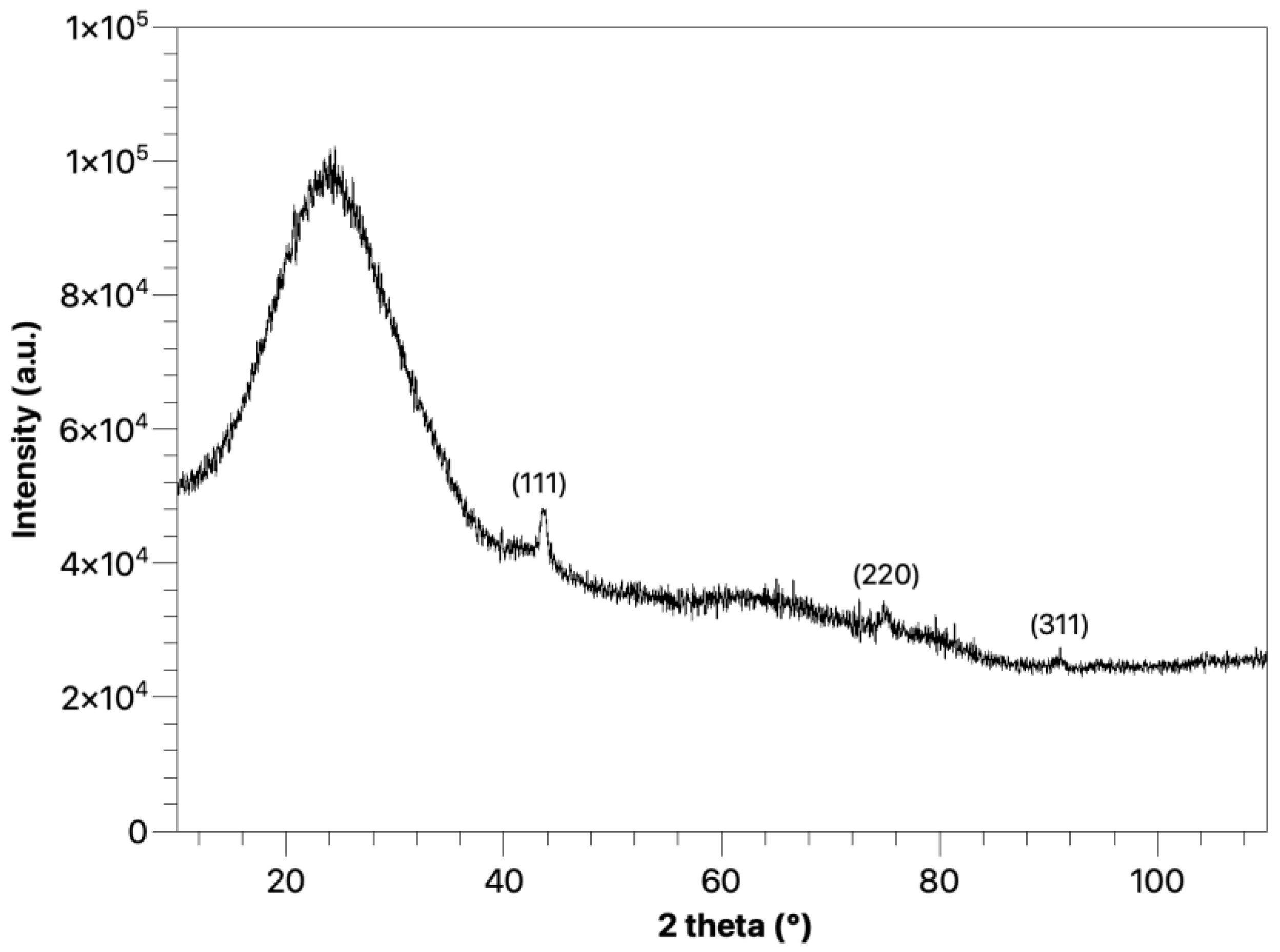
  33. Monshi, A.; Foroughi, M.R.; Monshi, M.R. Modified Scherrer equation to estimate more accurately nano-crystallite size using XRD. World J. Nano Sci. Eng. 2012, 2, 154. [Google Scholar] [CrossRef]
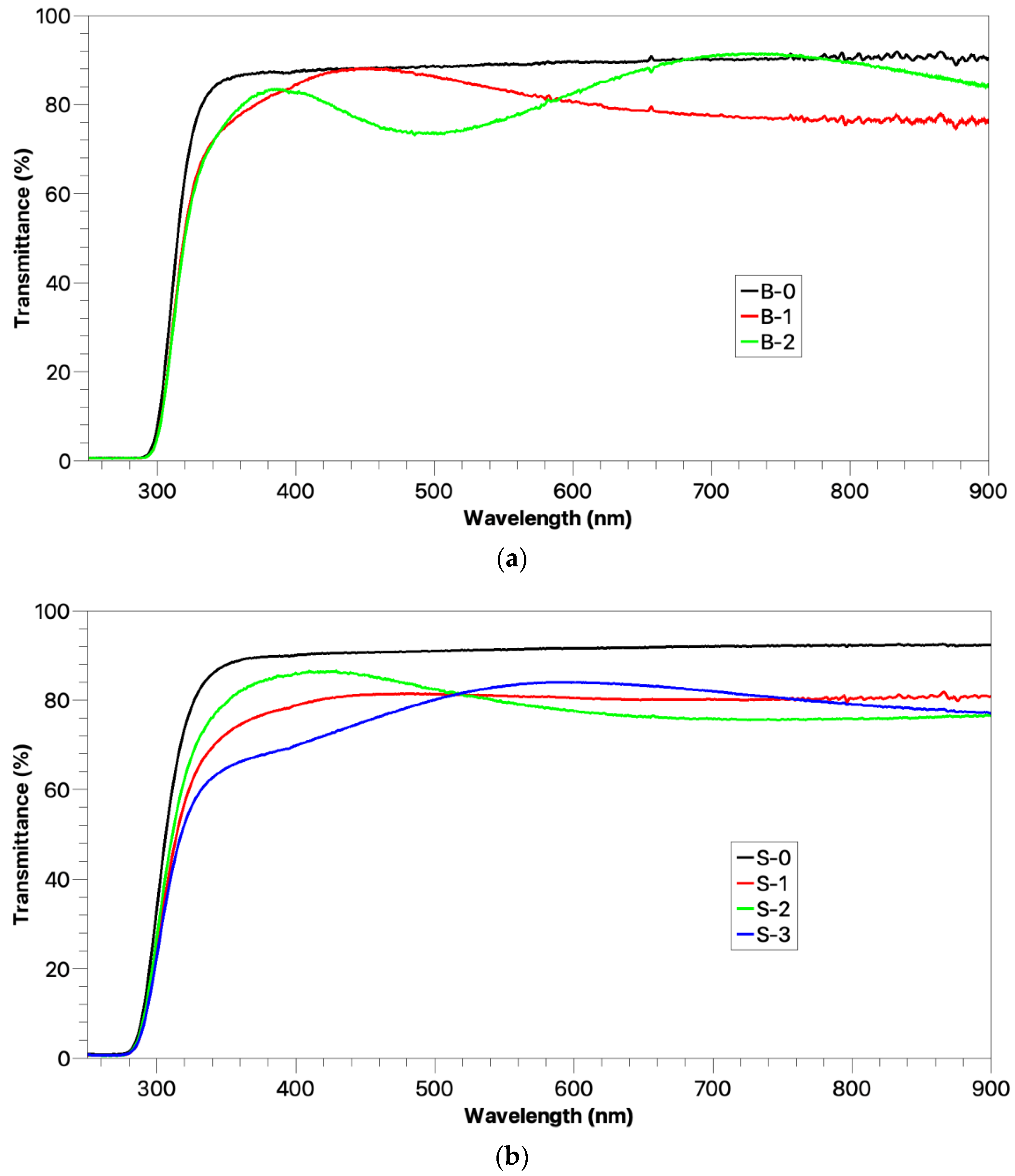
  34. Hassanien, A.S.; Akl, A.A.; El Radaf, I.M. Comparative studies for determining the optical band-gap energy of the novel polycrystalline thin ZnGa2S4 films sprayed at different film thickness. Research Sq. 2021. [Google Scholar] [CrossRef]
  35. Look, D.C.; Leach, J.H. On the accurate determination of absorption coefficient from reflectance and transmittance measurements: Application to Fe-doped GaN. J. Vac. Sci. Technol. B 2016, 34, 4–105. [Google Scholar] [CrossRef]
  36. Tauc, J. (Ed.) Amorphous and Liquid Semiconductors; Plenum Press: London, UK, 1974; p. 159. [Google Scholar]
  37. Tauc, J.; Grigorovici, R.; Vancu, A. Optical Properties and Electronic Structure of Amorphous Germanium. Phys. Status Solidi (B) 1966, 15, 627–637. [Google Scholar] [CrossRef]
  38. Suram, S.K.; Newhouse, P.F.; Gregoire, J.M. High throughput light absorber discovery, Part 1: An algorithm for automated Tauc analysis. ACS Comb. Sci. 2016, 18, 673–681. [Google Scholar] [CrossRef]
  39. Baudrillart, B.; Nave, A.S.C.; Hamann, S.; Bénédic, F.; Lombardi, G.; van Helden, J.H.; Röpcke, J.; Achard, J. Growth processes of nanocrystalline diamond films in microwave cavity and distributed antenna array systems: A comparative study. Diam. Relat. Mater. 2017, 71, 53–62. [Google Scholar] [CrossRef]
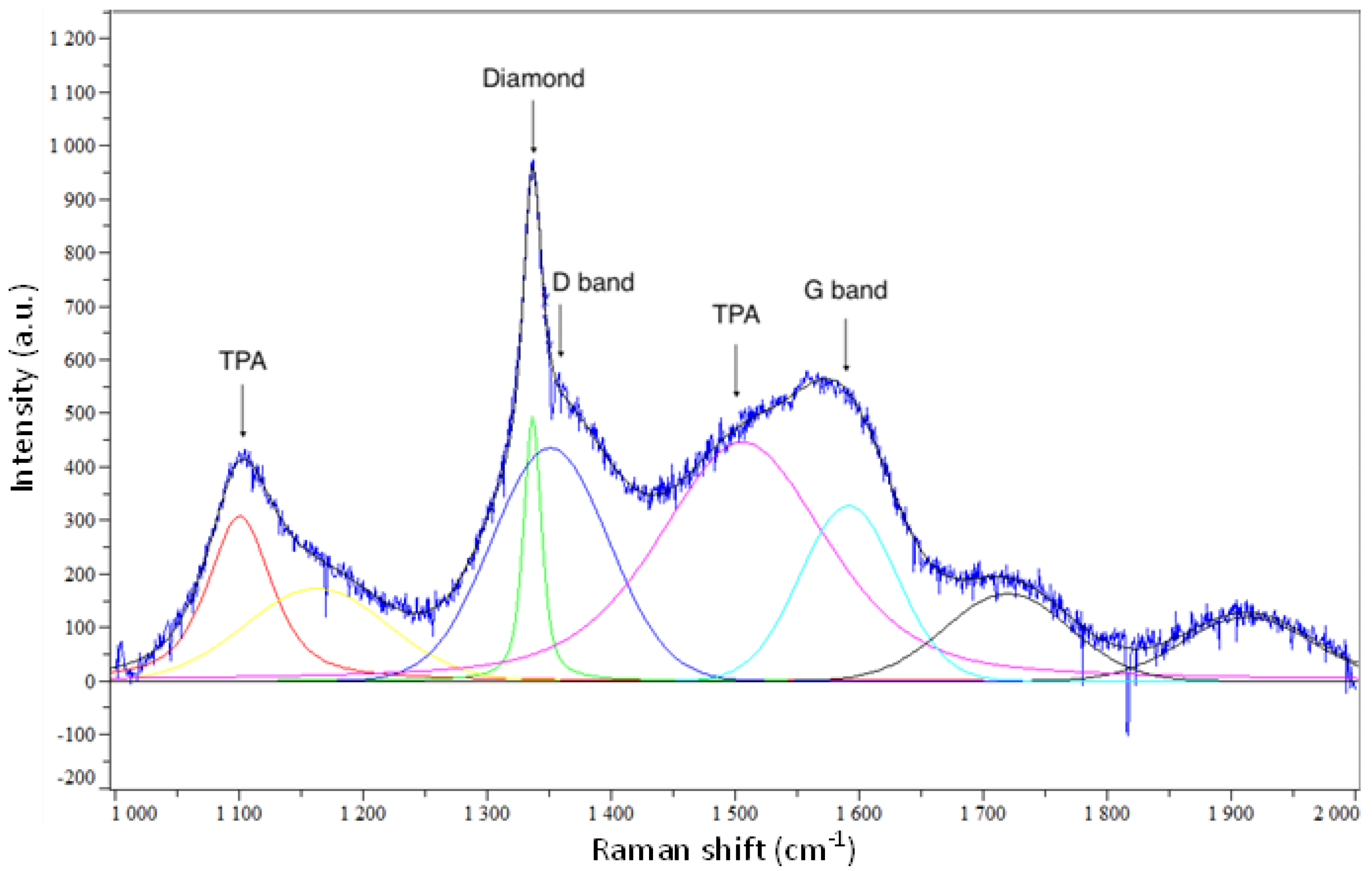
  40. Ferrari, A.C.; Robertson, J. Raman spectroscopy of amorphous, nanostructured, diamond-like carbon, and nanodiamond. Philos. Transact. A Math. Phys. Eng. Sci. 2004, 362, 2477–2512. [Google Scholar] [CrossRef]
  41. Ferrari, A.C.; Robertson, J. Origin of the 1150 cm−1 Raman mode in nanocrystalline diamond. Phys. Rev. B 2001, 63, 121405(R). [Google Scholar] [CrossRef]
  42. Pfeiffer, R.; Kuzmany, H.; Knoll, P.; Bokova, S.; Salk, N.; Günther, B. Evidence for trans- polyacetylene in nano-crystalline diamond films. Diam. Relat. Mater. 2003, 12, 268–271. [Google Scholar] [CrossRef]
  43. Hu, L.; Guo, Y.; Du, S.; Tian, S.; Li, J.; Gu, C. Probing trans-polyacetylene segments in a diamond film by tip-enhanced Raman spectroscopy. Diam. Relat. Mater. 2021, 116, 108415. [Google Scholar] [CrossRef]
  44. Barbosa, D.C.; Barreto, P.R.P.; Ribas, V.W.; Trava-Airoldi, V.J.; Corat, E.J. Diamond nanostructures growth. Encycl. Nanosci. Nanotechnol. 2009, 10, 3–10. [Google Scholar]
  45. Irshidat, M.R.; Al-Saleh, M.H.; Sanad, S. Effect of Nanoclay on Expansive Potential of Cement Mortar due to Alkali-Silica Reaction. ACI Mater. J. 2015, 112, 801. [Google Scholar] [CrossRef]
  46. Dekkar, D.; Bénédic, F.; Floer, C.; Hage-Ali, S.; Brinza, O.; Achard, J.; Elmazria, O. Study of Low Temperature Deposition of Nanocrystalline Diamond Films on ZnO/LiNbO3Layered Structures Suitable for Waveguiding Layer Acoustic Wave Devices. Phys. Status Solidi (A) 2018, 215, 1800251. [Google Scholar] [CrossRef]
  47. Haubner, R.; Lux, B. Deposition of ballas diamond and nano-crystalline diamond. Int. J. Refract. Met. Hard Mater. 2002, 20, 93–100. [Google Scholar] [CrossRef]
  48. Tsugawa, K.; Ishihara, M.; Kim, J.; Hasegawa, M.; Koga, Y. Large-Area and Low-Temperature Nanodiamond Coating by Microwave Plasma Chemical Vapor Deposition. New Diam. Front. Carbon Technol. 2006, 16, 14. [Google Scholar]
  49. Potocky, S.; Kromka, A.; Potmesil, J.; Remes, Z.; Polackova, Z.; Vanecek, M. Growth of nanocrystalline diamond films deposited by microwave plasma CVD system at low substrate temperatures. Phys. Status Solidi (A) 2006, 203, 3011–3015. [Google Scholar] [CrossRef]
  50. Potocky, S.; Kromka, A.; Potmesil, J.; Remes, Z.; Vorlicek, V.; Vanecek, M.; Michalka, M. Investigation of nanocrystalline diamond films grown on silicon and glass at substrate temperature below 400 °C. Diam. Relat. Mater. 2007, 16, 744–747. [Google Scholar] [CrossRef]
  51. Hu, Z.G.; Hess, P. Optical constants and thermo-optic coefficients of nanocrystalline diamond films at 30–500 °C. Appl. Phys. Lett. 2006, 89, 081906. [Google Scholar] [CrossRef]
  52. Williams, O.A. Nanocrystalline diamond. Diam. Relat. Mater. 2011, 20, 621–640. [Google Scholar] [CrossRef]
  53. Ralchenko, V.; Pimenov, S.; Konov, V.; Khomich, A.; Saveliev, A.; Popovich, A.; Vlasov, I.; Zavedeev, E.; Bozhko, A.; Loubnin, E.; et al. Nitrogenated nanocrystalline diamond films: Thermal and optical properties. Diam. Relat. Mater. 2007, 16, 2067–2073. [Google Scholar] [CrossRef]
  54. Wang, L.; Liu, J.; Ren, L.; Su, Q.; Shi, W.; Xia, Y. Effect of carbon concentration on the optical properties of nanocrystalline diamond films deposited by hot-filament chemical vapor deposition method. J. Nanosci. Nanotechnol. 2008, 8, 2534–2539. [Google Scholar] [CrossRef] [PubMed]
  55. Mertens, M.; Mohr, M.; Brühne, K.; Fecht, H.J.; Łojkowski, M.; Święszkowski, W.; Łojkowski, W. Patterned hydrophobic and hydrophilic surfaces of ultra-smooth nanocrystalline diamond layers. Appl. Surf. Sci. 2016, 30, 526–530. [Google Scholar] [CrossRef] [Green Version]
  56. Ostrovskaya, L.; Perevertailo, V.; Ralchenko, V.; Dementjev, A.; Loginova, O. Wettability and surface energy of oxidized and hydrogen plasma-treated diamond films. Diam. Relat. Mater. 2002, 11, 845–850. [Google Scholar] [CrossRef]
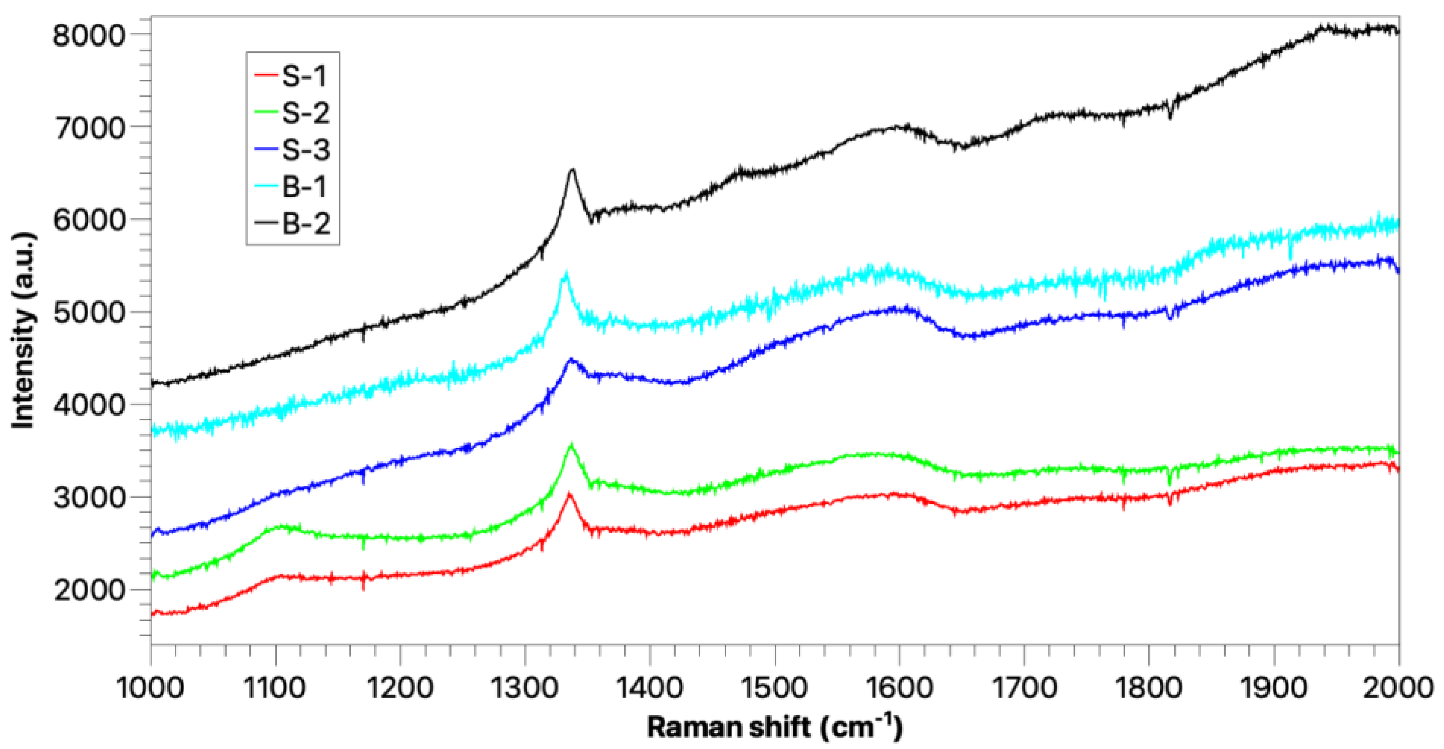
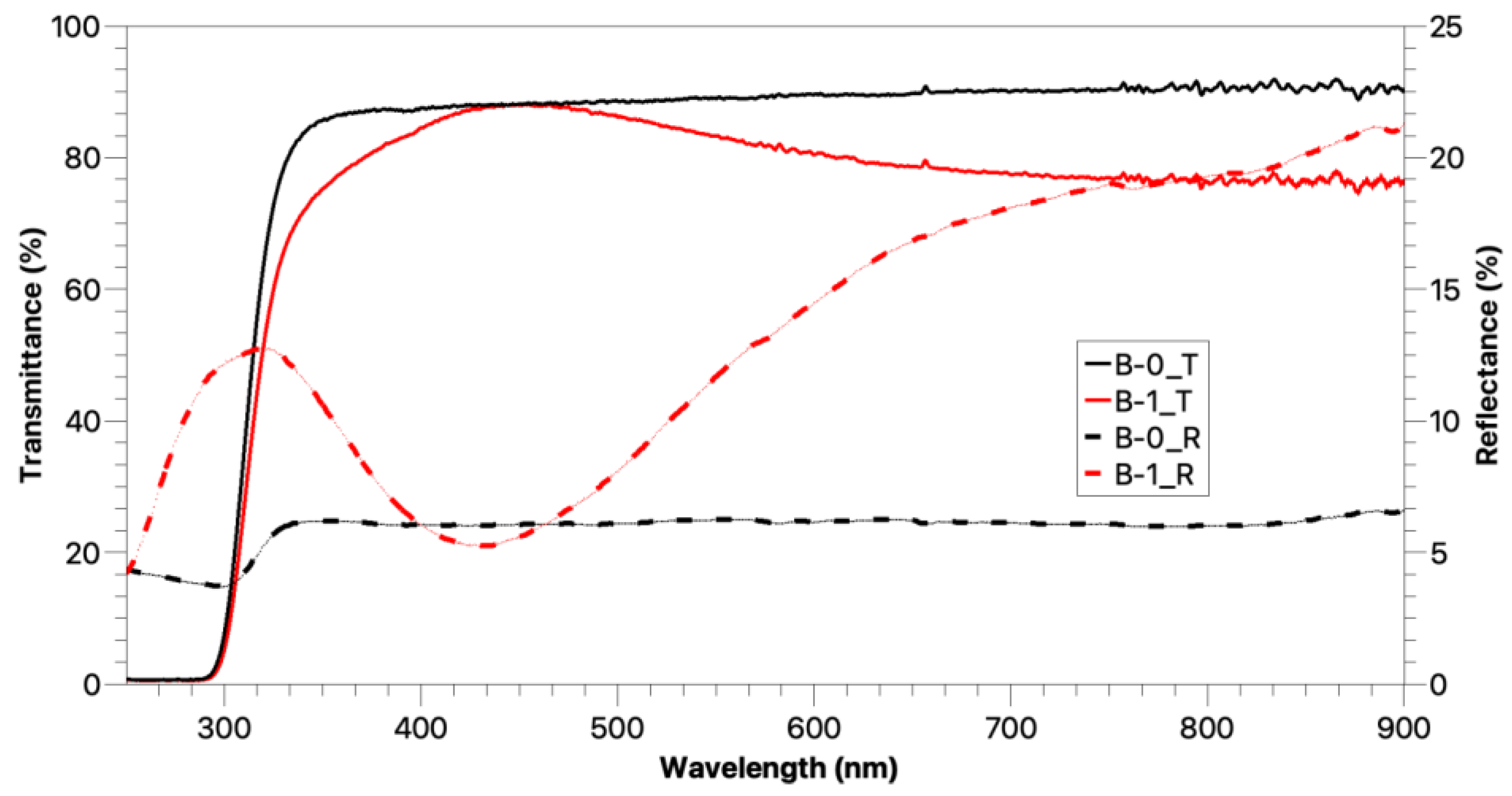
Figure 1. SEM micrographs of sample series B and S after NCD deposition.
Coatings 12 01375 g001
Figure 2. AFM micrographs of sample B-2 deposited at 300 °C during 4 h.
Coatings 12 01375 g002
Figure 3. Raman spectra of sample series B and S after NCD deposition.
Coatings 12 01375 g003
Figure 4. Deconvolution of the Raman spectrum of sample S-2 taking 8 contributions into account. The well-known trans-polyacetylene (TPA), graphite D and graphite G bands, and diamond peak, are indicated on the figure.
Coatings 12 01375 g004
Figure 5. XRD pattern of sample B-2 deposited at 300 °C during 4 h. The diamond diffraction peaks are indicated on the figure.
Coatings 12 01375 g005
Figure 6. Transmittance measured for glass substrates and NCD/glass systems: (a) sample series B, (b) sample series S.
Coatings 12 01375 g006
Figure 7. Transmittance (solid lines) and reflectance (dotted lines) measured for the borosilicate glass substrate (sample B-0) and the NCD/glass system after deposition (sample B-1).
Coatings 12 01375 g007
Figure 8. Calculated transmittance Tf and reflectance Rf of the NCD film deposited on sample B-1 at 300 °C during 2 h.
Coatings 12 01375 g008
Figure 9. Absorption coefficient α of the NCD film deposited on sample B-1 at 300 °C during 2 h. The inset figure shows the Tauc’s plot α h ν 1 2 vs. photon energy ( E = h ν ) for the considered sample. The straight line was used to determine the optical band gap E g .
Coatings 12 01375 g009
Table 1. Deposition conditions (substrate nature, deposition time, substrate temperature) and values of quantities reached from sample characterization (film thickness, growth rate, root mean square (Rms) roughness, diamond peak full width at half maximum (FWHM) and sp3 fraction from Raman spectra, contact angle) for sample series B and S.
SampleDeposition Time
(h)
Substrate Temperature
(°C)
Thickness
(nm)
Growth Rate
(nm·h−1)
Rms Roughness
(nm)
FWHM
(cm−1)
sp3
(%)
Contact Angle
(°)
B-0Uncoated substrate 2.0 + 0.4 54.3 ± 2.7
B-1230095 ± 948 ± 56.6 ± 1.317.5 ± 0.979 ± 876.0 ± 3.8
B-24153 ± 1538.3 ± 47.4 + 1.517.8 ± 0.982 ± 8
S-0Uncoated substrate 2.0 ± 0.4 40.5 ± 2.0
S-1226579 ± 839.5 ± 44.9 ± 1.016.8 ± 0.884 ± 8
S-2300104 ± 1052 ± 55.1 ± 1.017.2 ± 0.973 ± 776.5 ± 3.8
S-3400110 ± 1155 ± 610.5 ± 2.117.4 ± 0.959 ± 6
Publisher’s Note: MDPI stays neutral with regard to jurisdictional claims in published maps and institutional affiliations.

