Article

Epitaxial Growth and Optical Properties of Laser Deposited CdS Thin Films

by
Atef S. Gadalla
1,*,
Hamdan A. S. Al-shamiri
2,3,*,
Saad Melhi Alshahrani
4,
Huda F. Khalil
5,
Mahmoud M. El Nahas
6 and
Mohamed A. Khedr
1
1
National Institute of Laser Enhanced Science (NILES), Cairo University, Giza 12613, Egypt
2
Physics Department, Faculty of Science, University of Bisha, P.O. Box 551, Bisha 61922, Saudi Arabia
3
Physics Department, Faculty of Applied Science, Taiz University, Taiz P.O. Box 4007, Yemen
4
Chemical Department, Faculty of Science, University of Bisha, P.O. Box 551, Bisha 61922, Saudi Arabia
5
City of Scientific Research and Technological. Applications (SRTA-City), Electronics Material Dept., Alexandria 21933, Egypt
6
Physics Department, College of Education, Ain Shams University, Cairo 11566, Egypt
*
Authors to whom correspondence should be addressed.
Coatings 2022, 12(1), 87; https://doi.org/10.3390/coatings12010087
Submission received: 1 December 2021 / Revised: 5 January 2022 / Accepted: 6 January 2022 / Published: 13 January 2022
(This article belongs to the Special Issue 10th Anniversary of Coatings: Invited Papers for Thin Films Section)

Abstract

:
In this study, cadmium Sulfide (CdS) thin films were synthesized on quartz substrates using an infrared pulsed laser deposition (IR-PLD) technique under high vacuum (~10−6 Torr) conditions. X-ray diffraction was used to evaluate the structural features. According to X-ray analysis, the deposited CdS films are crystalline and have a favored orientation on a plane (110) of an orthorhombic. The peak intensity and the average crystallite size increases with increasing the film thickness. After annealing at 300 °C, the orthorhombic phase transformed into a predominant hexagonal phase and the same result was obtained by SEM photographs as well. Spectrophotometric measurements of transmittance and reflectance of the CdS films were used to derive optical constants (n, k, and absorption coefficient α). The optical band gap energy was found to be 2.44 eV. The plasma plume formation and expansion during the film deposition have also been discussed. The photocurrent response as a function of the incident photon energy E (eV) at different bias voltages for different samples of thicknesses (85, 180, 220 and 340 nm) have been studied, indicating that the photocurrent increases by increasing both the film thickness and photon energy with a peak in the vicinity of the band edge. Thus, the prepared CdS films are promising for application in optoelectronic field.

1. Introduction

Cadmium sulfide is a binary II-VI semiconductor consisting of the cadmium (Cd) element exclusive to group II and sulfide (S) to group VI of the periodic table. It has a direct band energy gap (2.42 eV) at room temperature (300 K). CdS is considered a promising material for a variety of optoelectronics applications, including photoluminescent, electroluminescent, photoconductive, and photovoltaic devices. The choice of its use is governed by the existing processing techniques and the properties that can be achieved under those conditions. The CdS thin film properties are strongly dependent on deposition method, rate of deposition, the substrate materials, temperature, and background pressure. The application and properties of the given material determine the most suitable technique for the preparation of thin films of the material. A variety of deposition techniques are suitable for producing thin films of CdS. These include chemical bath deposition (CBD) [1,2], electrodeposition [3], chemical spray pyrolysis (CSP) [4], successive ionic layer adsorption (SILA) [5], spin-coating [6], vacuum evaporation [7], screen printing [8], flash evaporation [9], sputtering [10], molecular beam epitaxy (MBE) [11], and pulsed laser deposition (PLD) [12,13]. Thin films prepared by these methods can differ significantly from each other in terms of their crystal structure, grain size, structural defects, and optical and electrical properties.
Some significant advantages of the PLD method, compared with other physical and chemical deposition techniques, areas follows: (I) it is simple and easy; (a laser beam vaporizes a target surface, resulting in a film with the same composition as the target); (II) many materials can be deposited in a variety of gases at a variety of pressures; (III) it is cost-effective (a single laser can power many vacuum systems); (IV) by controlling the parameters of the pulsed laser, the rate of growth and synthesis of nanoparticles can be controlled, as well as the kinetic energy of the evaporated species controlling the film growth modes and attributes; (V) it is scalable (in general, it is easier to obtain the desired film stoichiometry for multi-element materials using PLD than with other deposition technologies). Those unique merits make PLD suitable for the deposition of various high-quality thin films [14]. As a result, PLD can produce thin films of a variety of materials with strong adhesion such as insulators, metals, and semiconductors. In recent years, the pulsed laser deposition (PLD) technique has been widely developed and has become a suitable technique for the deposition of high-quality compound semiconductor thin films [15]. Recently the structure and optical and electrical properties of a cadmium sulfide (CdS) thin film prepared by pulsed laser deposition have attracted the attention of many authors due to its large field of applications [16,17,18]. There is also a demand for further development of thin films for minimization of the dimensions and weight of electronic systems. The fundamental advantage of generating CdS thin films through PLD at room temperature is that it allows for greater control over the structural, chemical, and electrical properties of the deposited material. It is important to note that other techniques present some difficulties in the modulation of certain parameters of the semi-conductor thin film.
In the present work, CdS films are synthesized by employing pulsed laser depositing (PLD) for their advantage as mentioned above. The deposition system consists of the evaporation source, with the fundamental wavelength for Nd: YAG Laser (1064 nm). The evaporation process depends on laser parameters such as laser energies and pulses duration [19], while the film thickness can be controlled to a single atomic layer by fine adjusting the pulse number. The deposition chamber is made of stainless steel, while the pumping system is composed of a rotary mechanical pump connected in series with a turbomolecular pump. This combination of the two pumps can reach a high vacuum pressure [20]. CdS thin films have been grown on quartz glass substrate at room temperature employing the pulsed laser deposition method. The effect of the number of laser pulses (film thickness) on the physical characteristics of CdS thin films has been studied. The main objective of the present work is to reach the optimum conditions by which the CdS thin film becomes more applicable in optoelectronic devices. This can be carried out by measuring the optical properties of IR-PLD CdS thin films in the wavelength range of 200–2500 nm and by studying the spectral distribution of photocurrent response at different incident photon energies.

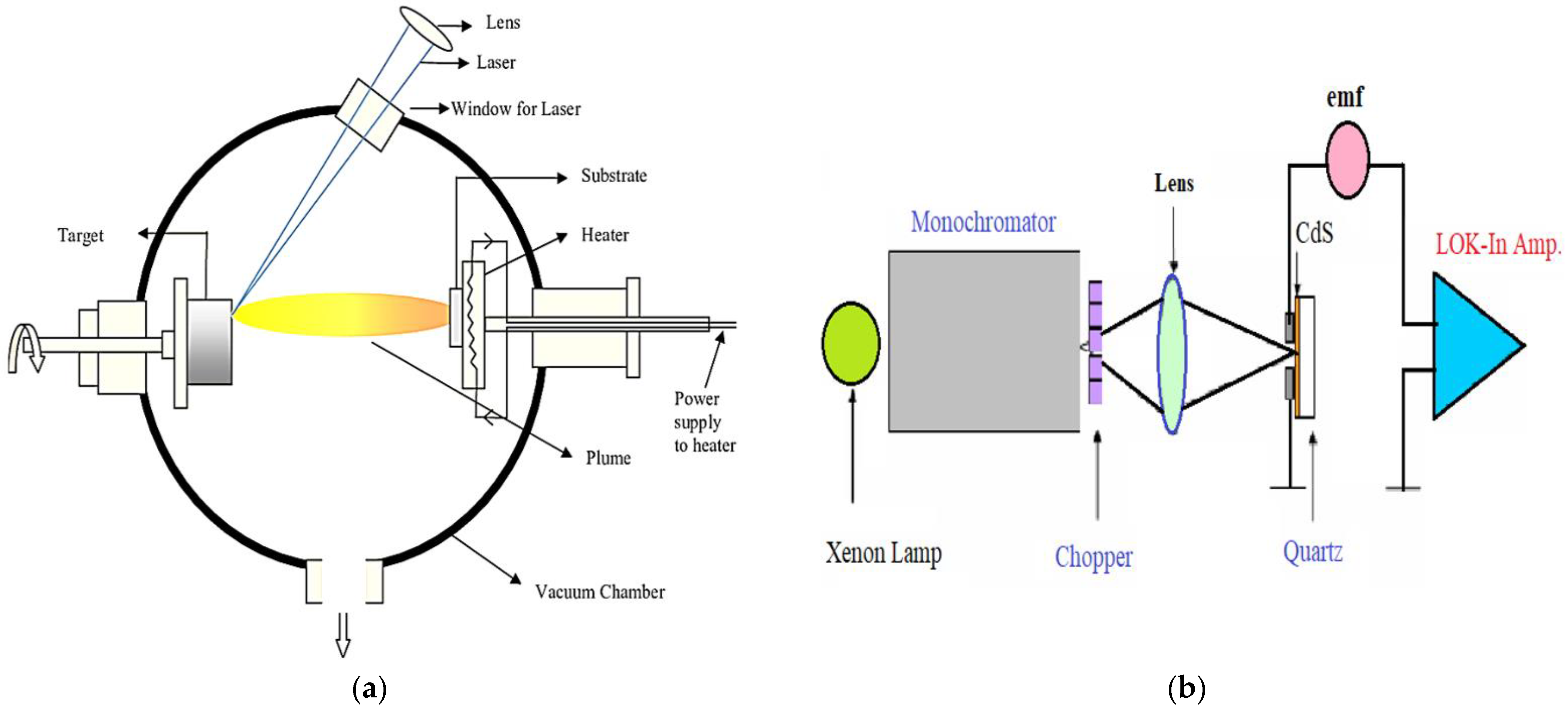
2. Experimental Details

2.1. Preparation CdS Thin Films

Cadmium Sulfide (CdS) thin films were deposited in a vacuum chamber using 1064 nm Nd-YAG laser (Model PL-7010) produced by Continuum. CdS is a semiconducting compound (II-VI) in the powder form with purity of 99% (BDH). The CdS targets were made in the form of pellets (10 mm in diameter and 3 mm in thickness) by grinding the material to be homogeneous fine powder and then compressed under high pressure of 8 × 10⁵ N/m2. A CdS target was mounted on a rotating target stage. The substrates were quartz glass placed 60 mm apart from the target surface. A schematic view of the film deposition setup is shown in Figure 1 as in [21].
Six samples of CdS thin film with different thickness were fabricated at room temperature. The vacuum chamber pressure was maintained ~10−6 Torr during the entire deposition process. The laser fluence was 4 J/cm2 and repetition rate was 10 Hz. The thickness of these six samples ranged from 60 to 340 nm.

2.2. Characterization Techniques

The film thickness was measured by the multiple beam Fizeau fringes method [22,23]. The X-ray diffraction patterns for CdS in the powdered and in thin film form for sample thickness 340 nm for as-deposited and after annealing at 300 °C were recorded automatically using Philips, Cu Kα radiation with λ = 1.54 Å. while the software Diano Corporation XSPEX (Woburn, MA, USA) and Fe filtered Co radiation with λ = 1.79 Å were used for X-ray diffraction patterns and line broadening of (110) plane for different thicknesses of CdS thin films, and compared with those given in the (JCPDS) card file (ICDD 77-2306). The detector is scintillated counter with a dead time of less than 10−6 s. The X-ray tube was energized at 45 kV and 10 mA.
A scanning electron microscope type JEOL 100S (JEOL, Tokyo, Japan) with a 60 kV operating voltage and a resolution of 50 Å with zero angle of sample inclination was used for study morphological surface of CdS films.
The spectrophotometric method was used for measuring the optical transmittance T and reflectance R of CdS thin films in the spectral range of 200–2500 nm. A UV/VIS/NIR double beam spectrophotometer (JASCO model V-570, Oklahoma, OK, USA) was used.
The plasma plume expansion during the film deposition was photographed by using a pinhole digital camera, and the spectral lines emitted from the plasma were collected from outside the vacuum chamber perpendicular to the direction of the laser beam by collimating lens through an optical fiber into a monochromator (CVI, Model CM-112) attached with a charge coupled device (CCD) camera controlled by a computer program.
Figure 1b shows a schematic diagram of an operation circuit of photocurrent measurements for CdS thin films. White light is shone from a xenon lamp (250 W) into a monochromator (Model 789A-3); the light then goes through a chopper and collimating lens into a thin film surface. Two indium electrodes are evaporated on the surface of the films and the distance between the two electrodes is 2 mm.
The external source (0–7 V) of the applied voltage is used and the photocurrent response is detected by a double channel lock-in amplifier (Model SR-530).

3. Results and Discussion

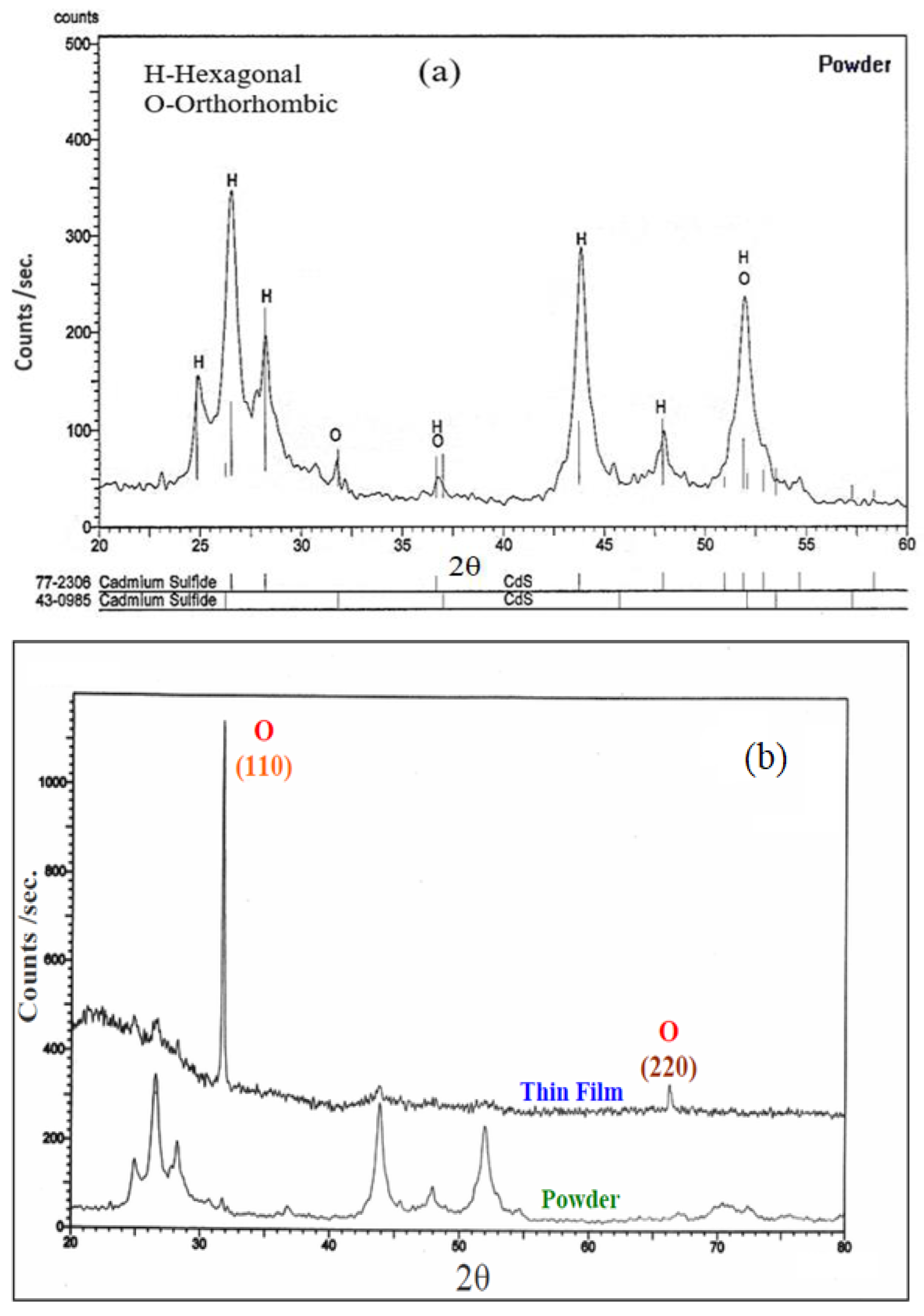
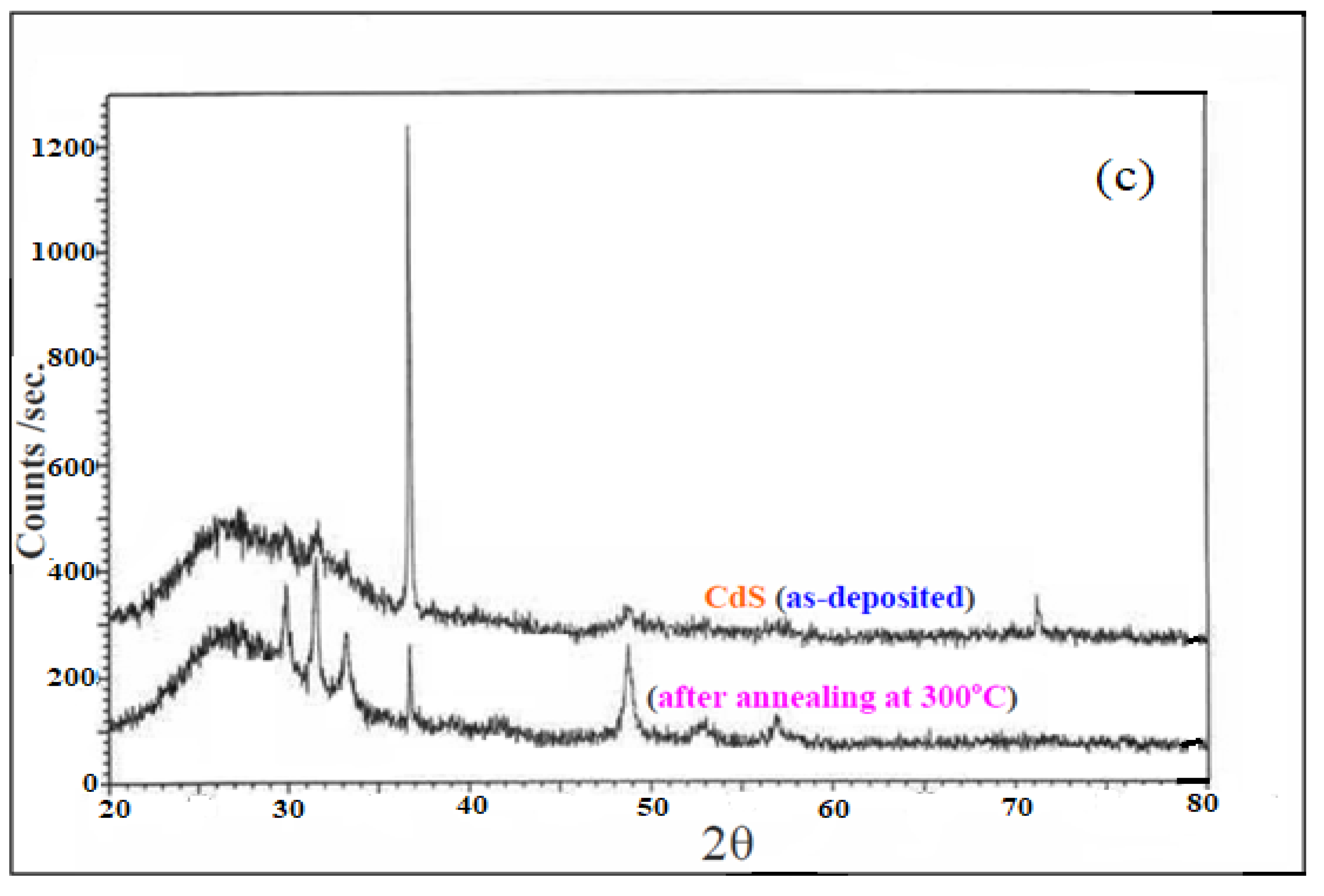
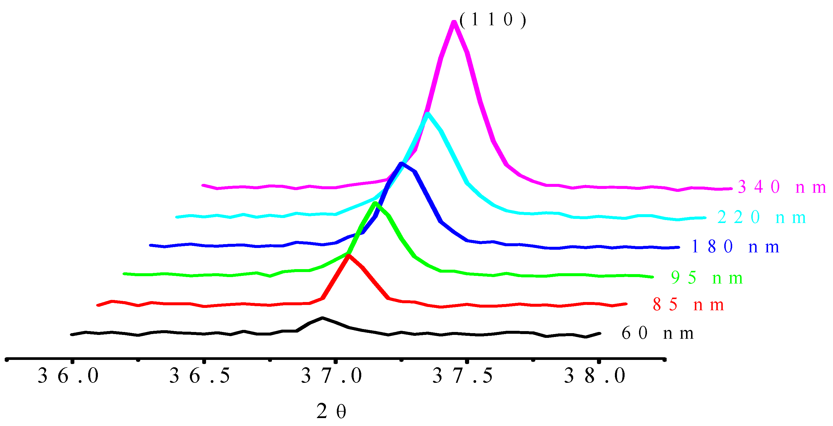
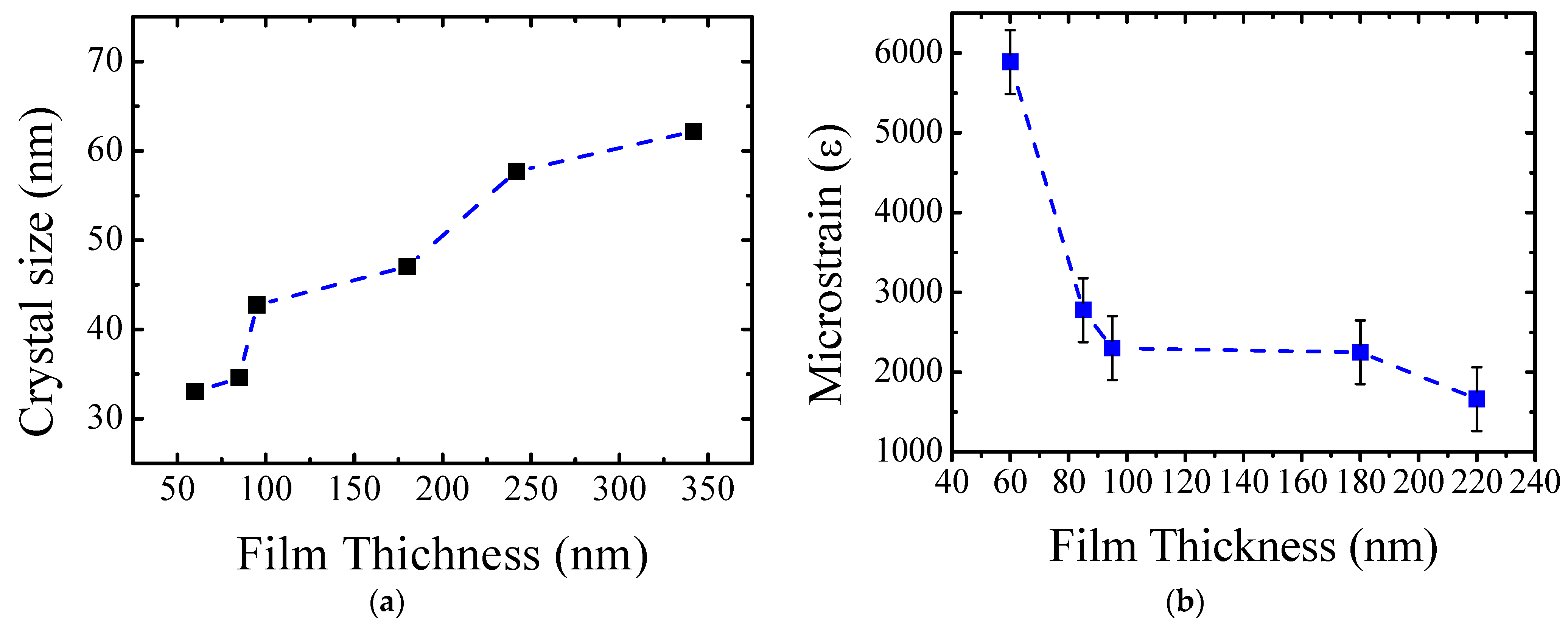
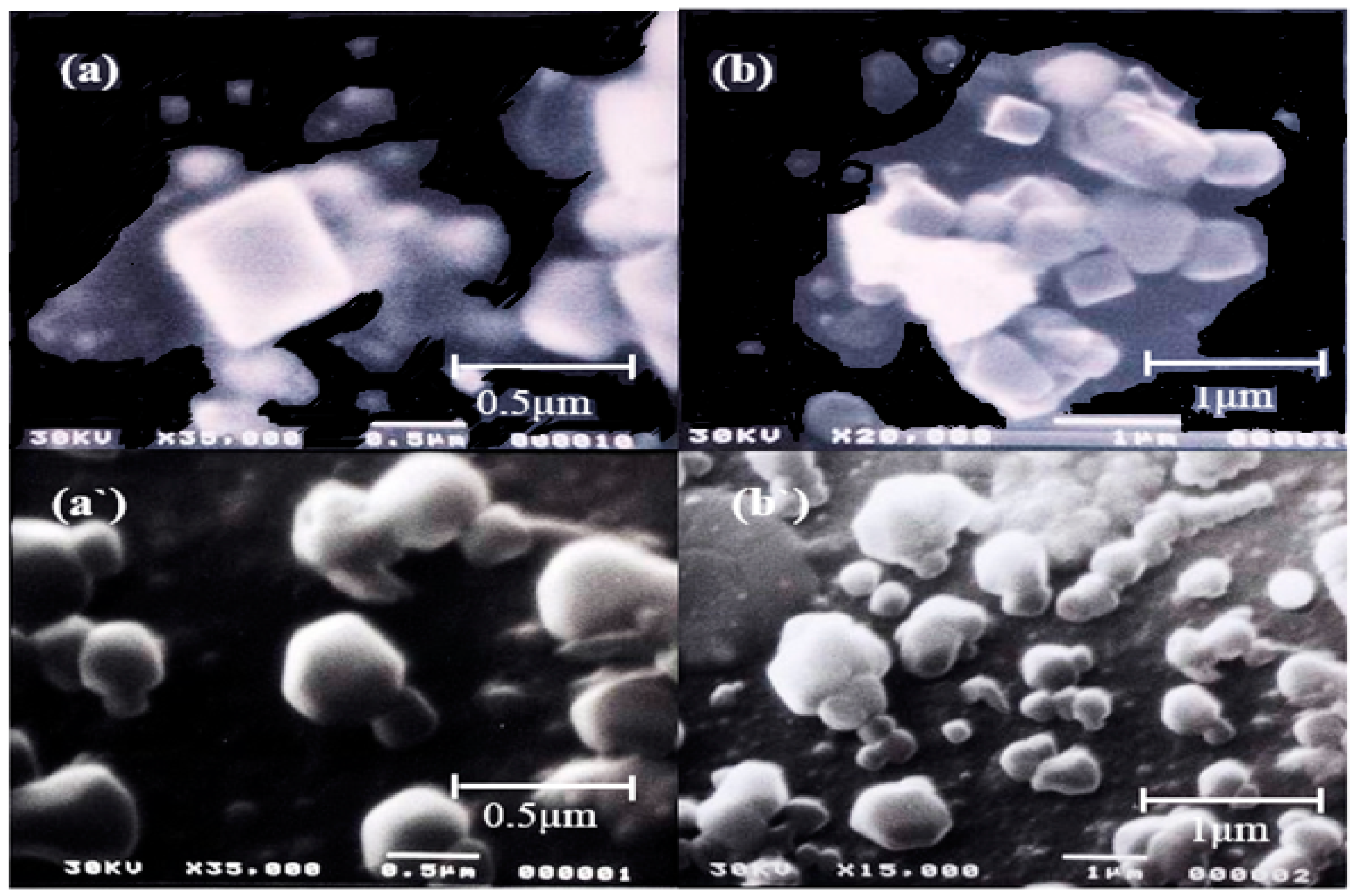
3.1. Structural Analysis

The XRD patterns of the CdS powder and thin films deposited under a vacuum (10−6 Tor) are shown in Figure 2. As represented in Figure 1a, there are two different phases (hexagonal and orthorhombic). The predominant phase is the hexagonal phase, as indicated from the peak intensities of the hexagonal one. The interplanar spacing (dhkl) were calculated using Diano Corporation XSPEX software and compared with those given in the (JCPDS) card file. Data representing the interplanar spacing (dhkl) and relative intensities I/Io for different (hkl) planes for CdS in the powder form, the as-deposited film, and the annealing film are given in Table 1. This indicates a polycrystalline nature of the powdered sample with lattice constants a = 4.136 Å and c = 6.713 Å for hexagonal form (ICDD 77-2306).
The X-ray pattern of the thin film shows a well-developed crystallographic texture (preferred orientation), where only two peaks (namely (110) and (220)) are clearly identified. Their d values are related to the orthorhombic phase (ICDD 43-0985), which agrees with that reported by V. V. Yakovlev et al. [24]. This means that the crystallites of the film are oriented in such a way that the (110) planes are parallel to the substrate surface. The data representing the interplanar spacing (dhkl) are given in Table 1.
Figure 2c shows the X-ray diffractograms for patterns of CdS thin film of thickness (340 nm) before and after annealing. When the sample was annealed at 300 °C for two hours, the X-ray pattern indicates that the intensity of the (110) plane was decreased and the (220) plane disappeared. Then, other peaks of the hexagonal form appear with considerable intensity (as shown in Figure 2b). This can be explained as that a part of the orthorhombic form is transformed into hexagonal one. The data in Table 1 show that most of the structure is hexagonal phase (ICDD 77-2306) with its characteristic peaks, and this is consistent with the SEM photographs of CdS as shown in Figure 5a,b.
The resulting X-ray diffractograms for as-deposited CdS thin films with different thicknesses ranged from 60 to 340 nm are represented in Figure 3. All films showed preferred orientation parallel to (110) direction, and the peak intensity increased with increasing film thickness where no shift in the peak position (2θ = 37°) was observable.
X-ray line broadening of the (110) reflection of the as-deposited CdS thin films with different thicknesses is represented in Figure 3. The crystallite size and micro-strain as a function of film thickness are determined and represented in Figure 4a, b, respectively. From Figure 4a, it is observed that the average crystallite size increases with increasing the film thickness. The observation of A. Amith [25] and J. B. Wilson [26] regarding the increase of crystallite size with increasing of the film thickness agrees well with our results. A large number of Cd2+ and S2+ ions increase with increasing the film thickness and get adsorbed on the substrate. Filling the voids leads to an increase in the value of crystallite size, and the defects in the lattice are reduced, which in turn reduces the micro-strain [27] as shown in Figure 4b. In addition, the microstrain (ε) of the films decreases as the films thickness increases. This gives an indication of low imperfections and high- quality crystal geometry.
With the increase in the film thickness and the exposure of the material to laser pulses, the number of ions present increases, and therefore the deposition process increases which lead to filling the interstitial voids in the material. The film thickness from 60 to 100 nm the intermolecular space is large and leads to a sharp decrease of microstrain (which may be a result of a nonlinear relation). After increasing the thickness from 100 to 220 nm, the intermolecular spaces were decreased, and the motion freedom of the ions decreased, which led to little change of microstrain. The relation between the thin film thickness and microstrain is a linear relation as shown in Figure 4b.
The standard deviations for the relation between microstrain versus film thickness as shown in Figure 4b were calculated and tabulated in Table 2.
It is noticeable that the standard deviation increased directly with the increased film thickness and inversely with microstrain. This result fits with the crystal size calculation and the increase of the deposition process.
Scanning electron microscope (SEM) micrographs represented in Figure 5a,b shows the orthorhombic form for the as-deposited CdS thin films.

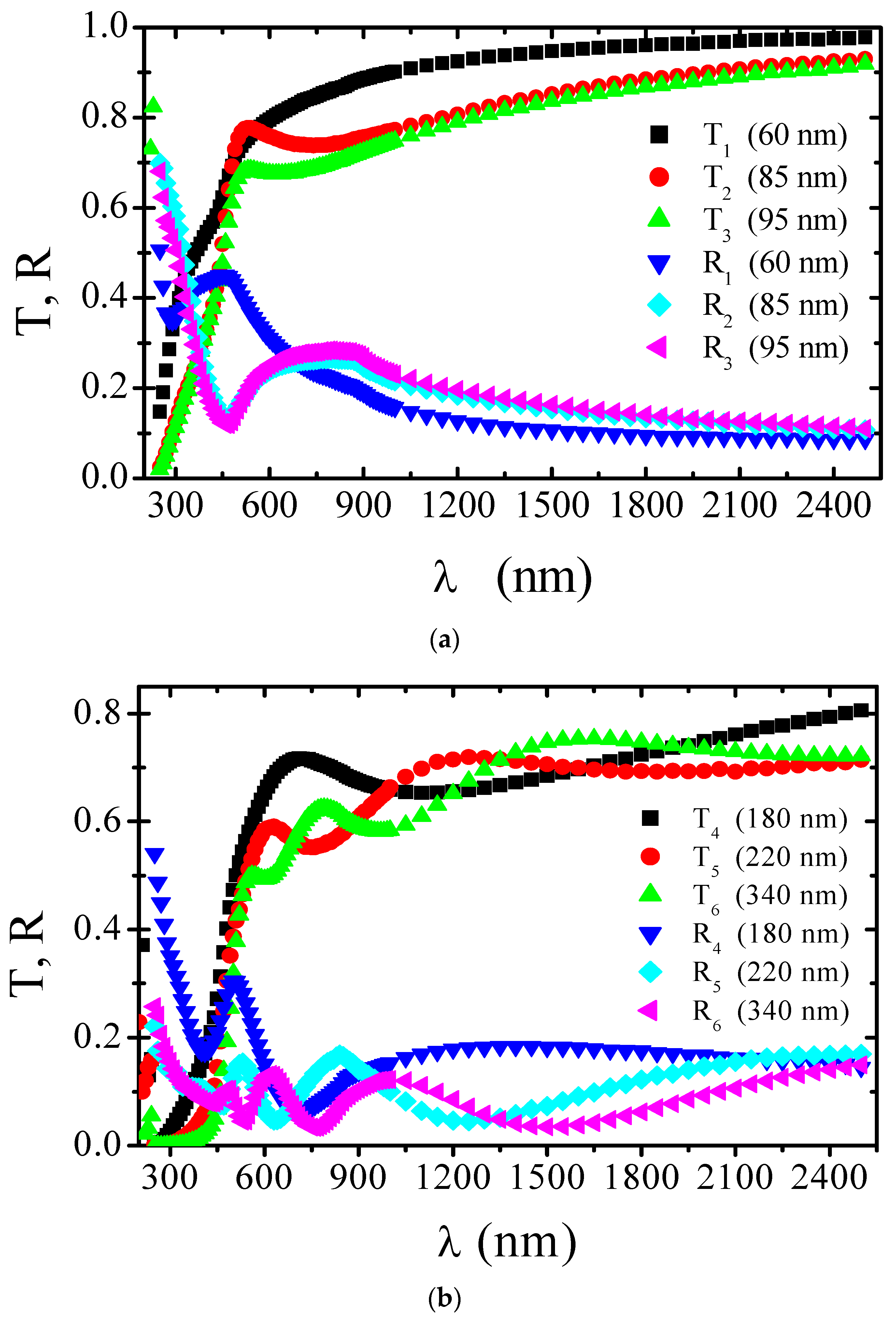
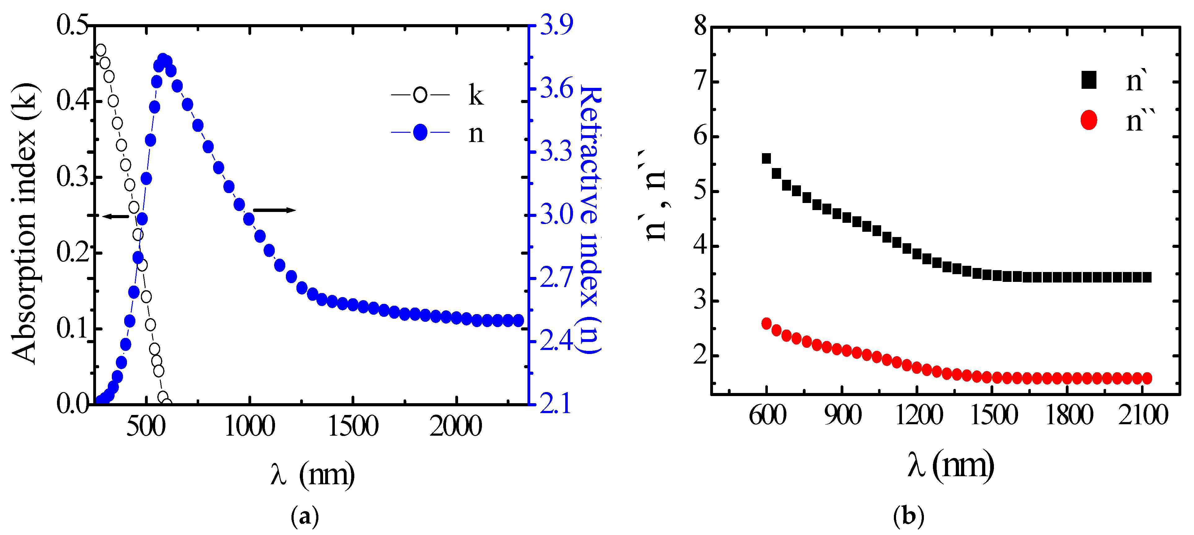
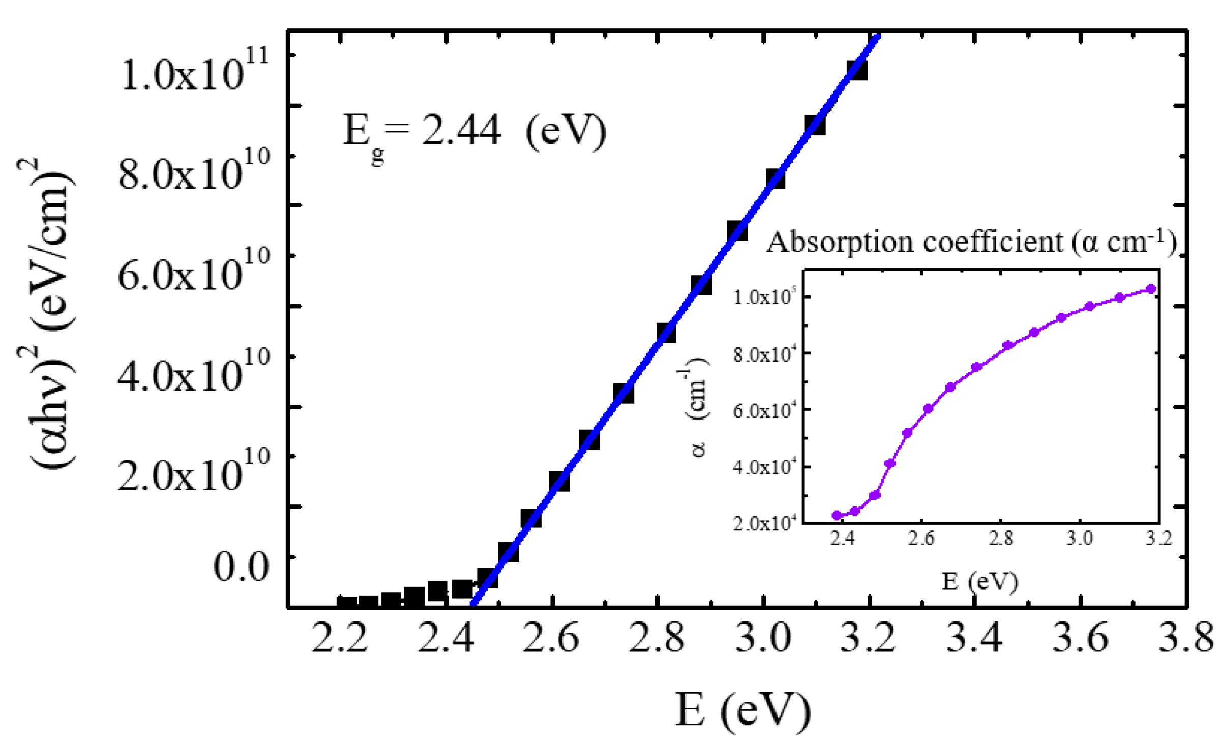
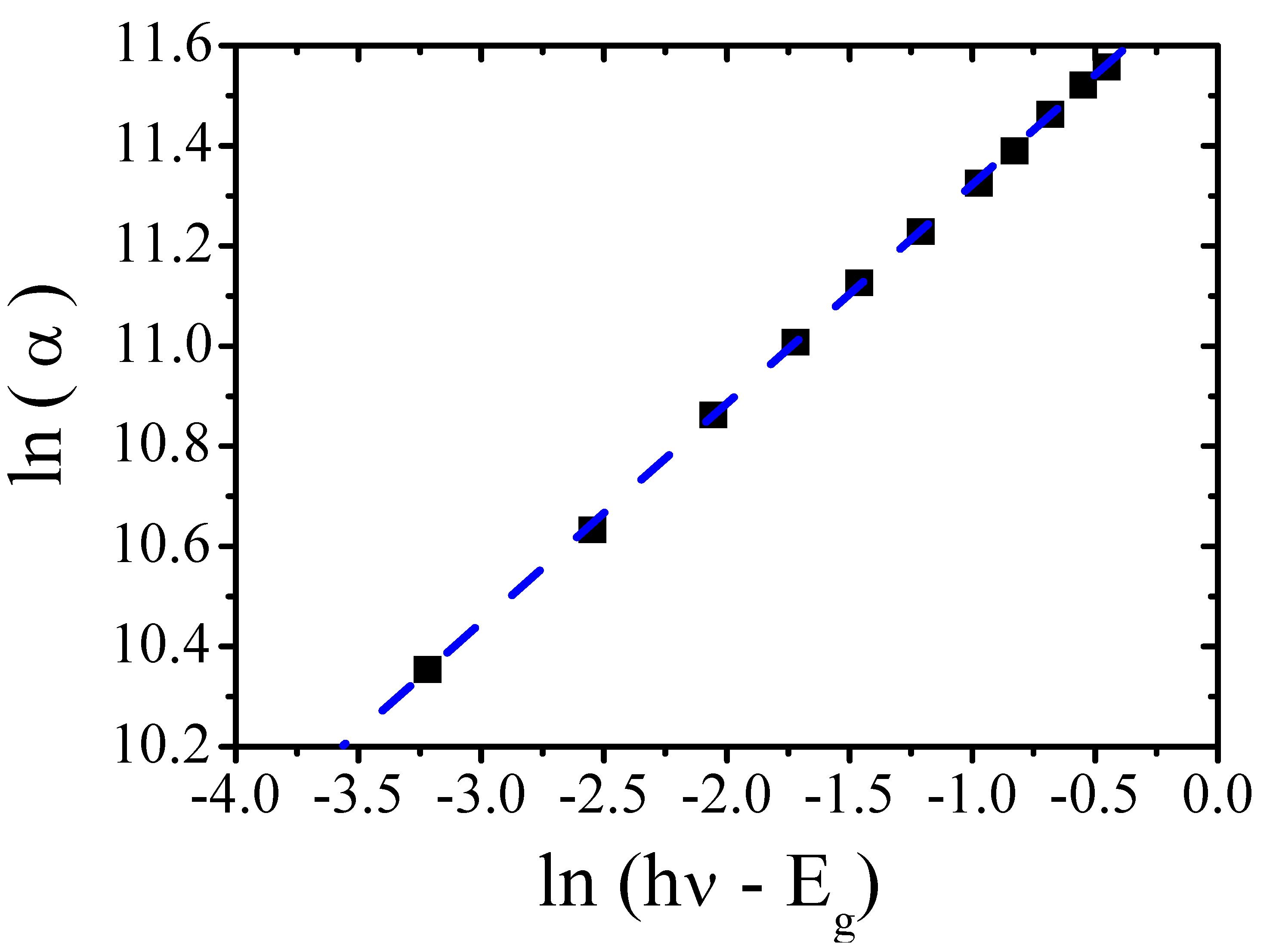
3.2. Optical Properties

The transmittance (T) and the reflectance (R) for each film were measured by spectrophotometric method at normal incidence of light in the spectral range 200–2500 nm.
The spectral behavior of transmittance, T(λ), and reflectance, R(λ), for six different thicknesses of CdS films, are shown in Figure 6a,b. There are homogeneous CdS thin films in the thickness range (60–95 nm) Figure 6a, the others inhomogeneous films in the thickness range (180–340 nm), Figure 6b.
The transmittance for all CdS films decreases with the increasing of the thickness (which, in turn, increases with the increasing of the wavelength).
The spectral behavior of refractive index n(λ) and absorption index k(λ) for the homogeneous CdS films represents Figure 7. The obtained results of both n(λ) and k(λ) show that these parameters are independent of the film thickness in the thickness range (60–340 nm). The fluctuation in both n(λ) and k(λ) can be attributed to the experimental errors in T, R and the film thickness (d). The curve behaves like a normal dispersion above λ = 1500 nm and shows anomalous dispersion towards a shorter wavelength. The peak that appears in the spectral distribution of the refractive index is due to a rapid increase in the absorption mechanism in the fundamental absorption edge [28]. No variations in (n) with the film thickness could be observed in the utilized film thickness ranges. The error in calculated values of (n) was estimated to be 3% due to experimental error for measuring T, R = ±0.01%, and film thickness = 2%.
The absorption coefficient, (α) of as-deposited CdS thin films was calculated using the equation:
α ( λ ) = 4 π k λ
where k; the mean value of the absorption index at a particular wavelength. The spectral behavior of the absorption coefficient (α) versus photon energy (hν) and the (αhυ)2 as a function of hυ for as-deposited CdS films are shown in Figure 8. The optical transitions in semiconductors can be represented by
α h ν = A ( h ν E g ) m
where m = 0.5 in case of allowed direct optical transitions [29]. The relation yields a straight line indicating allowed direct optical transitions where Eg = 2.44 eV. To confirm the existence of the allowed direct optical transitions in CdS thin film, ln(α) is plotted as a function of ln (hυ − Eg) as shown in Figure 9. One linear relation is obtained having a slope = 0.5, indicating and confirming the allowed direct optical transitions.

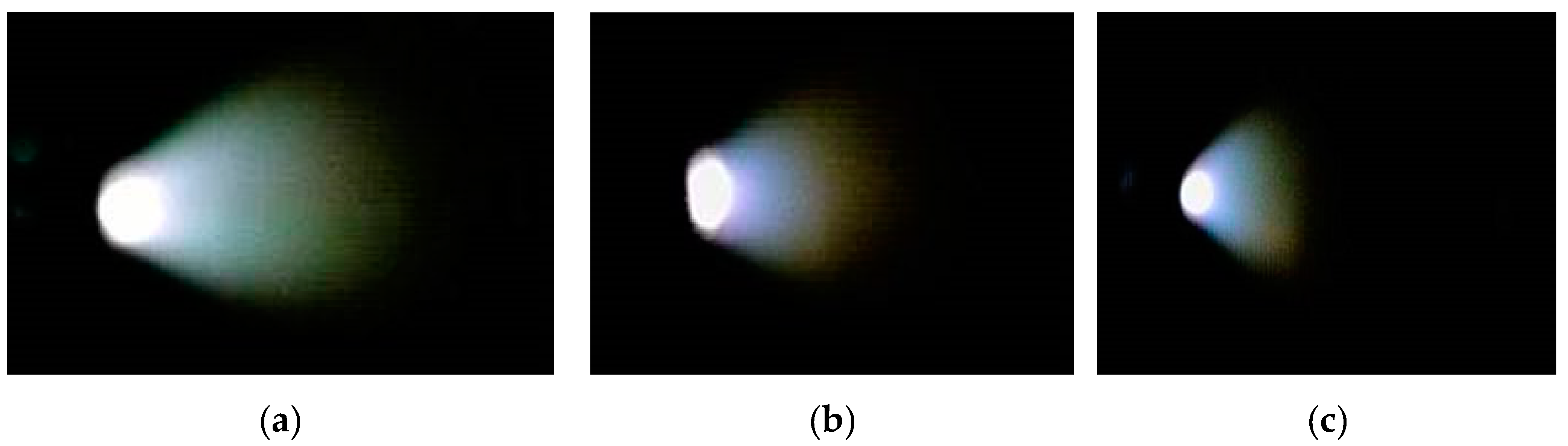
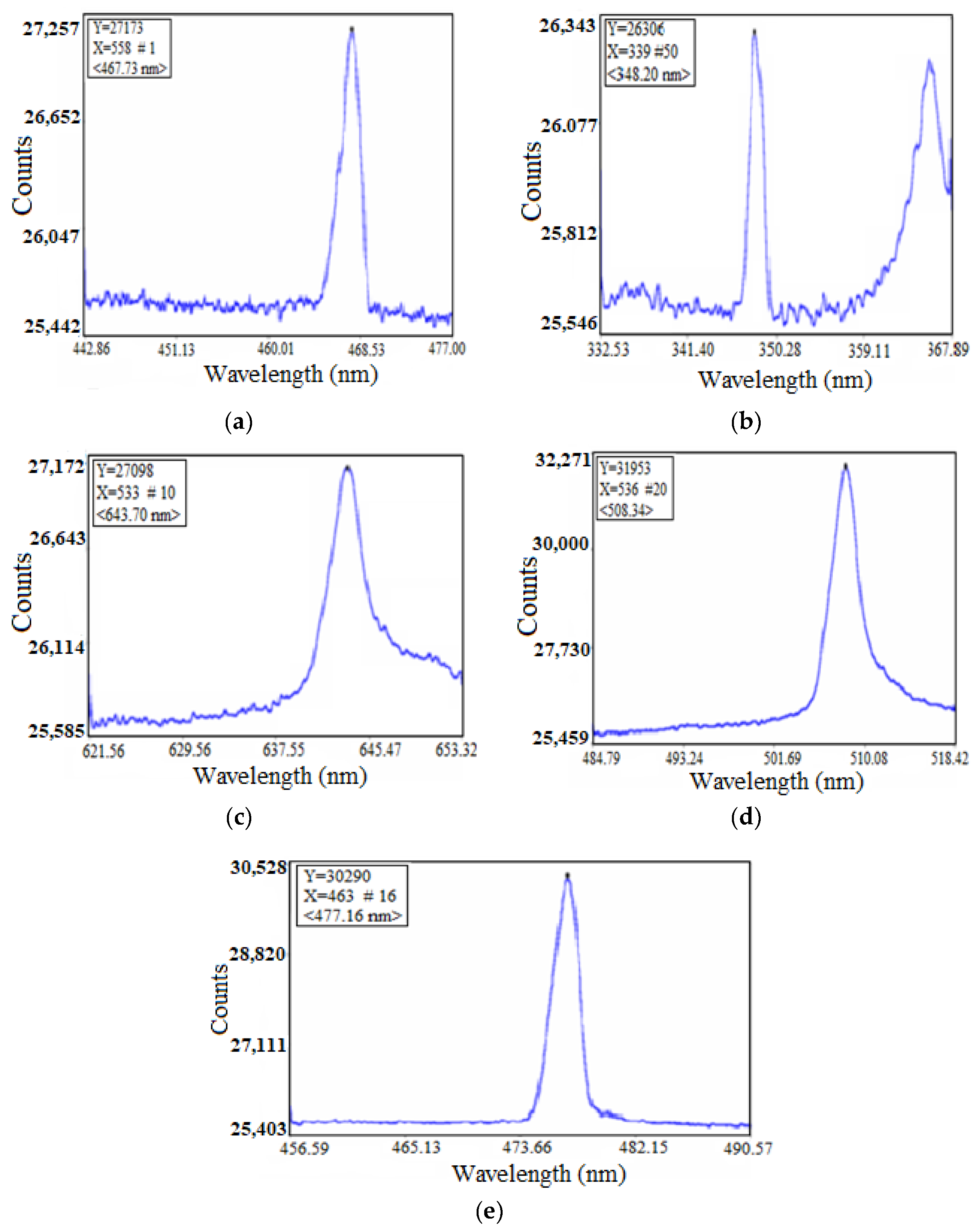
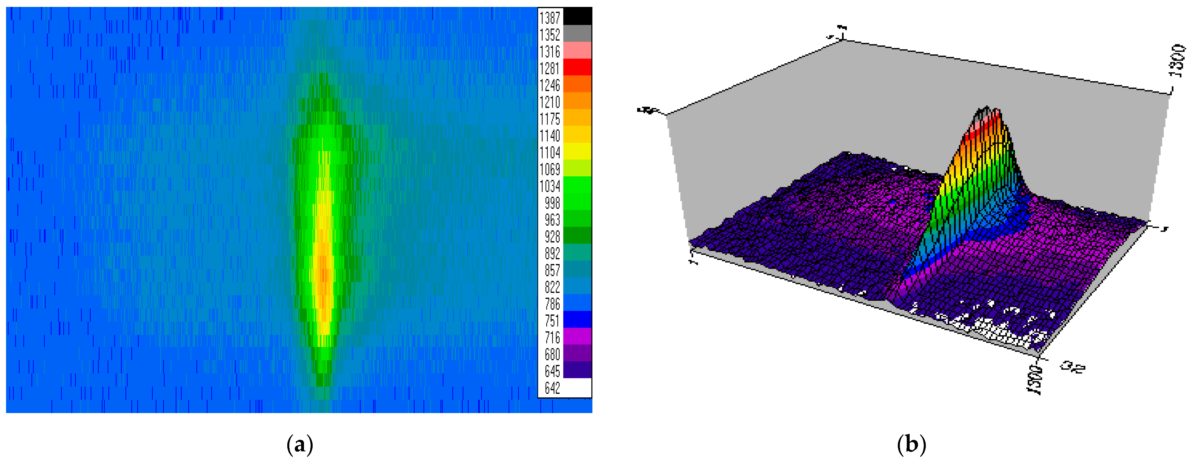
3.3. Plasma Plume and Spectral Profiles

Plasma produced by the focusing of laser beam on solid targets became the object of intensive theoretical and experimental studies immediately after high power lasers became available [30].
Different diagnostic techniques, such as optical spectroscopy [31,32], Laser-induced fluorescence [33], have been used in attempts to characterize the plasma as it expands either in a vacuum or in an ambient atmosphere. The laser beam is concentrated to a spot of 0.5 mm in diameter on the CdS target surface with an angle of incidence 0°. Expansions of the plasma plumes were observed and photographed by using a pinhole digital camera, when the Nd: YAG laser beam of wavelength 1064 nm impinges onto a CdS target surface, the plasma expands perpendicularly to the target surface independently of the angle of incidence.
After a certain number of laser shots, the depth of the hole increases with the number of laser pulses. By rotating the target to get a new target surface, the direction of the plasma plume turns increasingly towards the incident laser beam, as shown in Figure 10a. By increasing the hole depth, the observed plasma plume outside the hole becomes shorter, and the intensity of the emission decreases, as indicated in Figure 10b, c. When the laser beam interacts with the plasma plume, some of its energy is absorbed by the atoms, exiting them. Electrons are pushed into high energy states (only to later fall back down to lower states). When this transition occurs, radiation is emitted at a specific frequency. The emitted spectra were recorded from a side window using a monochromator attached with a charge-coupled device (CCD) camera controlled by a computer program through an optical fiber. Spectra were taken at different distances from the target surface.
Figure 11a–e shows the emission spectra from a CdS target. There is a broadening in the emission lines due to both frequent causes, namely the spectrometer having 0.5 nm resolution, and physical causes such as a “Doppler shift” due to atomic movement and the effect of atomic collisions in the target plume.
The image profile and three-dimensional profile of the spectral line 477.16 nm are shown in Figure 12a,b.
Unfortunately, most of the emission lines of the Cd2+ made up the plasmas lies in the ultraviolet region of the electromagnetic spectrum outside the range of our spectrometer but most of the S2+ lines are detected and were compared with the known emission lines [34] as represented in Table 3.

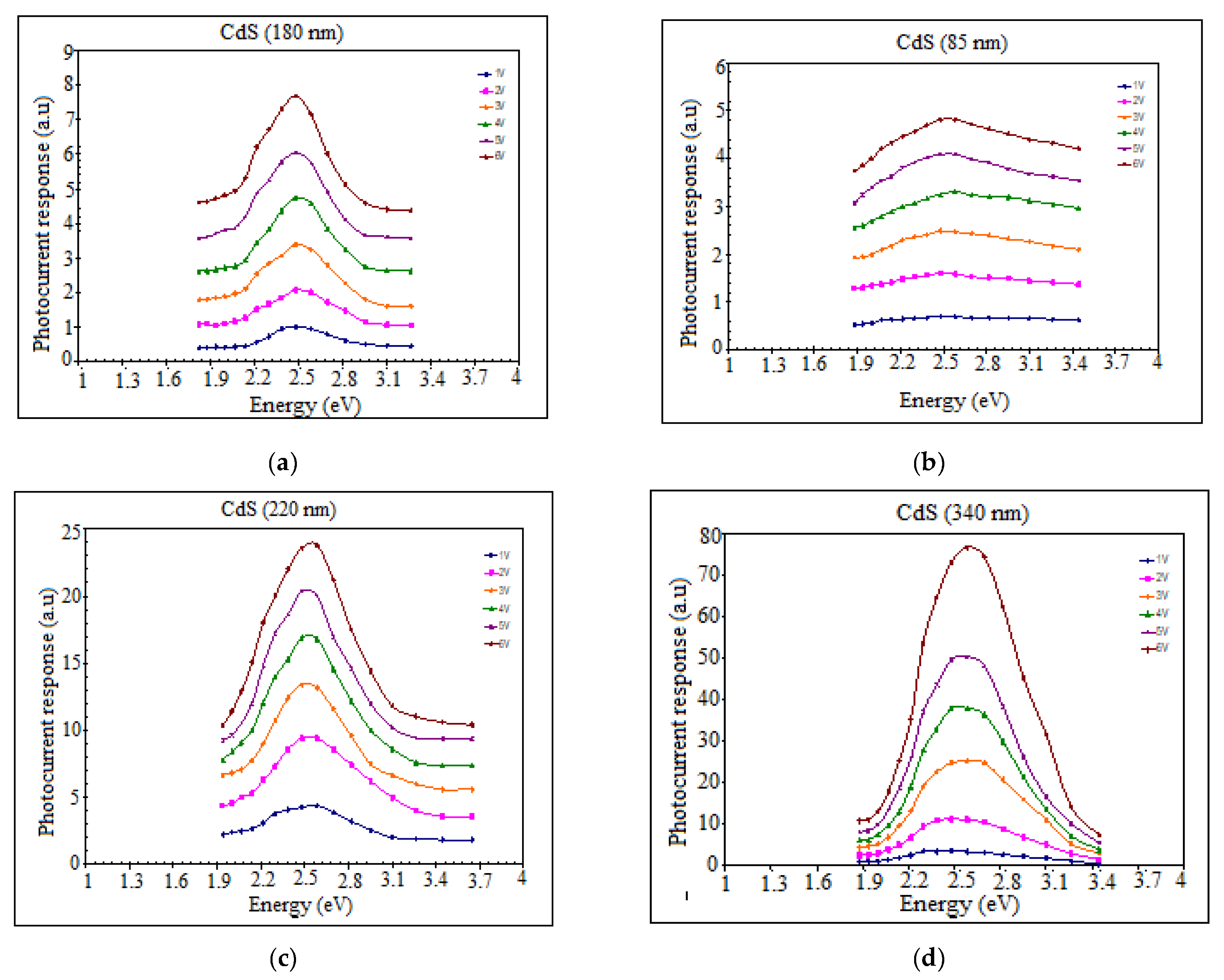
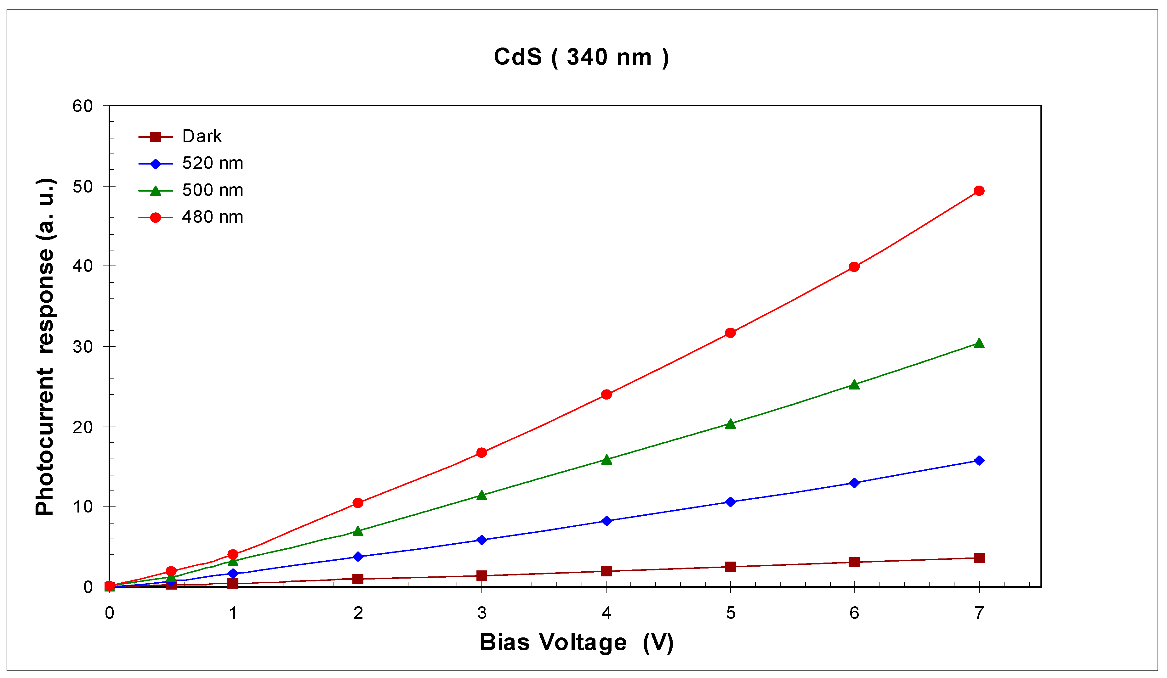
3.4. Photoconductivity Response

The spectrum of the CdS thin films by a different bias voltage (1–6 V) was characterized with the photon energy, E (eV), as shown in Figure 13a–d. The samples for each thickness 85, 180, 220, and 340 nm, respectively, display increasing of the photocurrent response by raising the incident photon energy E (eV), with a peak in the vicinity of the band edge. This can be attributed to the generation of a greater number of free charge carriers in the bandgap region, and this is probably connected with the grain boundary, which induces an electric field due to the spatial distribution of electrons in the grain [35]. The optimized as-deposited CdS thin film at thickness 340 nm exhibits the high energy at voltage 6 V and photocurrent approximately 80.
Figure 14 shows the voltage dependence of the dark current and photocurrent recorded for the as-deposited CdS thin film of 340 nm. The dark current and the photocurrent increase straightly with the increase in the applied voltage in the region studied (0–7 V), and the photocurrent is greater than the dark current at the same bias voltage.
In darkness, the photoconductor resistance is very high, and when a voltage is applied, only a small dark current was observed. When light is incident on this photoconductor, a current (I) flows due to the generation of a greater number of charge carriers.
Here are the basic principles of the photoconductive effect [36]: (Ι) directly beneath the conduction band of the CdS crystal is a donor level, and there is an acceptor level above the valence band. In darkness, the electrons and holes in each level are almost crammed in place in the crystal and the photoconductor is at high resistance; (ΙΙ) when light illuminates the CdS film surface and is absorbed, the electrons in the valence band are excited into the conduction band. This creates pairs of free holes in the valence band and free electrons in the conduction band, increasing the conductance; (ΙΙΙ) furthermore, near the valence band is a separate acceptor level that can capture free electrons only with difficulty but captures free holes easily. This lowers the recombination probability of the electrons and holes and increases the number of electrons in the conduction band for n-type conductance. Until the carriers generated in (ΙΙ) and (ΙΙΙ) recombine, electrons are injected from one electrode and pulled out by the other. When these carriers last longer and they move more, the conductance increases greatly.

4. Conclusions

The X-ray analysis of the prepared CdS thin films shows that all films crystalline with an orthorhombic system have a preferred orientation in the (110) direction. The peak intensity of the plane (110) increases with increasing the film thickness. After annealing at 300 °C for the sample of thickness 340 nm, the X-ray diffraction pattern indicates that the orthorhombic phase is transformed into a predominant hexagonal phase, and this was confirmed by SEM photographs. The average crystallite size of the films increased with increasing film thickness due to the increase in the number of Cd2+ and S2+ ions, which became adsorbed on the substrate and began filling the voids. It increased the crystallite size value, and the defects in the lattice were reduced, which reduced the microstrain in the samples. The cadmium sulfide followed the direct allowed transition with Eg = 2.44 eV. The direction of the plasma plume expansion was perpendicular to the target surface, and the plume length decreased with an increase of the number of incident laser pulses. The photocurrent increased with the expanding of the film thickness, and this is likely due to the growth of crystallinity of thin films resulting from expanding the film thickness.

Author Contributions

Almost all of the authors participated by the same effort in terms of preparing the thin films, making measurements, discussing, analyzing the results, and writing as in the presented form. All authors have read and agreed to the published version of the manuscript.

Funding

This research received no external funding.

Institutional Review Board Statement

Not applicable.

Informed Consent Statement

Not applicable.

Data Availability Statement

Data is contained within the article.

Conflicts of Interest

The authors declare no conflict of interest.

References

  1. Wilson, K.; Ahamed, M.B. Surface modification of cadmium sulfide thin film honeycomb nanostructures: Effect of in situ tin doping using chemical bath deposition. Appl. Surf. Sci. 2016, 361, 277–282. [Google Scholar] [CrossRef]
  2. Perlikowski, I.; Zielony, E.; Özdal, T.; Kavak, H. Structural properties and electrical characteristics of p-n junctions based on kesterite cu2znsns4 layers for thin-film solar cells. Energies 2021, 14, 5182. [Google Scholar] [CrossRef]
  3. Zhang, Y.; Ma, H.; Wu, D.; Li, R.; Wang, X.; Wang, Y.; Zhu, W.; Wei, Q.; Du, B. A generalized in situ electrodeposition of Zn doped CdS-based photoelectrochemical strategy for the detection of two metal ions on the same sensing platform. Biosens. Bioelectron. 2016, 77, 936. [Google Scholar] [CrossRef] [PubMed]
  4. Yılmaz, S.; Atasoy, Y.; Tomakin, M.; Bacaksız, E. Comparative studies of CdS, CdS: Al, CdS: Na and CdS:(Al–Na) thin films prepared by spray pyrolysis. Superlattices Microstruct. 2015, 88, 299. [Google Scholar] [CrossRef]
  5. Kim, W.; Baek, M.; Yong, K. Fabrication of ZnO/CdS, ZnO/CdO core/shell nanorod arrays and investigation of their ethanol gas sensing properties. Sens. Actuators B Chem. 2016, 223, 599–605. [Google Scholar] [CrossRef]
  6. Özdal, T.; Chtouki, T.; Kavak, H.; Figa, V.; Guichaoua, D.; Erguig, H.; Mysliwiec, J.; Sahraoui, B. Effect of annealing temperature on morphology and optoelectronics properties of spin coated CZTS thin films. J. Inorg. Organomet. Polym. Mater. 2021, 31, 89. [Google Scholar] [CrossRef]
  7. Trajic, J.; Gilic, M.; Romcevic, N.; Romcevic, M.; Stanisic, G.; Hadzic, B.; Petrovic, M.; Yahia, Y. Raman spectroscopy of optical properties in CdS thin films. Sci. Sinter. 2015, 47, 145. [Google Scholar] [CrossRef]
  8. Croitoru, N.; Jakobson, S. Properties of CdS films and Cu2S-CdS junctions prepared by chemical printing. Thin Solid Films 1979, 56, L5–L7. [Google Scholar] [CrossRef]
  9. Canevari, V.; Romeo, N.; Sberveglieri, G.; Azzi, S.; Tosi, A.; Curti, M.; Zanotti, L. Low resistivity CdS thin films grown by flashǦ evaporation at low substrate temperature (150–200 °C). J. Vac. Sci. Technol. A 1984, 2, 9–10. [Google Scholar] [CrossRef]
  10. Piel, A.; Murray, H. Etude de la conduction Poole-Frenkel dissymétrique dans des structures Al-CdS-Au. Thin Solid Films 1977, 44, 65–73. [Google Scholar] [CrossRef]
  11. Shay, J.L.; Wagner, S.; Bettini, M.; Bachmann, K.J.; Buehler, E. InP—CdS solar cells. IEEE Trans. Electron Devices 1977, 24, 483–486. [Google Scholar] [CrossRef]
  12. Bleu, Y.; Bourquard, F.; Tite, T.; Loir, A.; Maddi, C.; Donnet, C.; Garrelie, F. Review of graphene growth from a solid carbon source by pulsed laser deposition (PLD). Front. Chem. 2018, 6, 572. [Google Scholar] [CrossRef] [PubMed] [Green Version]
  13. Elhmaidi, Z.O.; Abd-Lefdil, M.; El Khakani, M.A. Photoconversion optimization of pulsed-laser-deposited p-CZTS/n-Si-nanowires heterojunction-based photovoltaic devices. Nanomaterials 2020, 10, 1393. [Google Scholar] [CrossRef] [PubMed]
  14. Kossowsky, R.; Jelinek, M.; Novak, J.; Jelínek, M.; Trtík, V.; Jastrabík, L. Pulsed laser deposition of thin films. In Physics and Materials Science of High Temperature Superconductors, IV; Kossowsky, R., Jelinek, M., Novák, J., Eds.; Springer: Dordrecht, The Netherlands, 1997. [Google Scholar]
  15. Ogugua, S.N.; Ntwaeaborwa, O.M.; Swart, H.C. Latest development on pulsed laser deposited thin films for advanced luminescence applications. Coatings 2020, 10, 1078. [Google Scholar] [CrossRef]
  16. Martínez-Landeros, V.H.; Hernandez-Como, N.; Gutierrez-Heredia, G.; Quevedo-Lopez, M.A.; Aguirre-Tostado, F.S. Structural, chemical and electrical properties of CdS thin films fabricated by pulsed laser deposition using varying background gas pressure. Thin Solid Films 2019, 682, 24–28. [Google Scholar] [CrossRef]
  17. Abd, J.A.; Mohammed, W.M.; Al-Nafiey, A. CdS nanostructured thin films synthesized by pulsed laser deposition for solar cell technology. Key Eng. Mater. 2021, 882, 155–164. [Google Scholar] [CrossRef]
  18. Hussein, W.S.; Ahmed, A.F.; Aadim, K.A. Influence of laser energy and annealing on structural and optical properties of CdS films prepared by laser induced plasma. Iraqi J. Sci. 2020, 61, 1307–1312. [Google Scholar] [CrossRef]
  19. Hernandez-Como, N.; Martinez-Landeros, V.; Mejia, I.; Aguirre-Tostado, F.S.; Nascimento, C.D.; de Azevedo, G.M.; Krugc, C.; Quevedo-Lopez, M.A. Defect control in room temperature deposited cadmium sulfide thin films by pulsed laser deposition. Thin Solid Films 2014, 550, 665–668. [Google Scholar] [CrossRef]
  20. Moore, J.H.; Davis, C.C.; Coplan, M.A. Building Scientific Apparatus: A practical Guide to Design and Construction; Preseus Books: New York, NY, USA, 1991. [Google Scholar]
  21. Mittra, J.; Abraham, G.J.; Kesaria, M.; Bahl, S.; Gupta, A.; Shivaprasad, S.M.; Viswanadham, C.S.; Kulkarni, U.D.; Dey, G.K. Role of substrate temperature in the pulsed laser deposition of zirconium oxide thin film. Mater. Sci. Forum 2012, 710, 757–761. [Google Scholar] [CrossRef]
  22. Tolansky, S. Multiple-Beam Interference Microscopy of Metals; Academic Press: London, UK, 1970. [Google Scholar]
  23. Tolansky, S. Multiple-Beam Interferometry of Surface and Films; Oxford University: London, UK, 1978. [Google Scholar]
  24. Yakovlev, V.V.; Lazarov, V.; Reynolds, J.; Josifovska, M.G. Laser-induced phase transformations in semiconductor quantum dots. Appl. Phys. Lett. 2000, 76, 2050. [Google Scholar] [CrossRef]
  25. Amith, A. Thickness dependence of structural and electrical properties of Cds films for solar cells. J. Vac. Sci. Technol. 1978, 15, 353. [Google Scholar] [CrossRef]
  26. Wilson, J.B.; Woods, J. The electrical properties of evaporated films of cadmium sulphide. J. Phys. Chem. Sol. 1973, 34, 171. [Google Scholar] [CrossRef]
  27. Mahalingam, T.; John, V.S. Microstructural characterization of electrosynthesized ZnTe thin films. Cryst. Res. Technol. 2002, 37, 329. [Google Scholar] [CrossRef]
  28. Ioffe, A.F. Physics of Semiconductor, 491; Info Search Limited: London, UK, 1957. [Google Scholar]
  29. Heavens, O.S. Optical Properties of Thin Solid Films; IOP Publishing: London, UK, 1955. [Google Scholar]
  30. Atwee, T.; Kunze, H.-J. Spectroscopic investigation of two equal colliding plasma plumes of boron nitride. J. Phys. 2002, 35, 524. [Google Scholar]
  31. Morrow, T.; Sakeek, H.F.; El-Astal, A.; Walmsley, D.G.J. Absorption and emission spectra of the YBCO laser plume. J. Supercond. Nov. Magn. 1994, 7, 823. [Google Scholar] [CrossRef]
  32. Wang, X.T.; Man, B.Y.; Hu, X.Y. Optical spectroscopy of plasma produced by laser ablation of Ti alloy in air. J. Appl. Phys. 1996, 80, 1783. [Google Scholar] [CrossRef]
  33. Brackmann, C.; Nygren, J.; Bai, X.; Li, Z.; Bladh, H.; Axelsson, B.; Denbratt, I.; Koopmans, L. Per-Erik Bengtsson Marcus Aldén Laser-induced fluorescence of formaldehyde in combustion using third harmonic Nd. YAG Laser Excit. 2003, 59, 33347. [Google Scholar]
  34. Kramida, A.; Ralchenko, Y.; Reader, J.; NIST ASD. 2020 NIST Atomic Spectra Database (Ver.5.8) [online September 2021, Spectrmmeter] National Institute of Standards and Technology Gaithrs. Available online: https://www.nist.gov/pml/atomic-spectra-database (accessed on 26 September 2021).
  35. Dutta, J.; Bhattacharyya, D.; Chdhuri, A.S.; Pal, A.K. Cadmium sulfide thickness effect on the photoresponse of the CdS(A1) spray/poly(3-methylthiophene) solid state junction. Sol. Energy Mater. Sol. Cells 1993, 29, 209. [Google Scholar]
  36. Heijne, L. Physical Principles of photoconductivity. Philips Tech. Rev. 1963, 25, 120. [Google Scholar]
Figure 1. (a) The schematic diagram of pulsed laser deposition system. (b) Experimental setup for AC Photocurrent.
Coatings 12 00087 g001
Figure 2. (a) Typical X-ray diffraction patterns as powder form. (b) In powder and thin film forms. (c) As-deposited and after annealing thin film at 300 °C.
Coatings 12 00087 g002aCoatings 12 00087 g002b
Figure 3. X-ray of IR-PLD CdS thin films with different thicknesses.
Coatings 12 00087 g003
Figure 4. Crystal size (a), Microstrain (b) of CdS thin films as a function of film thickness.
Coatings 12 00087 g004
Figure 5. (a,b) SEM micrographs of as-deposited IR-PLD CdS thin film, (a`,b`) SEM micrographs of IR-PLD CdS thin film annealing at 300 °C.
Coatings 12 00087 g005
Figure 6. Transmittance and reflectance curves of (a) homogeneous CdS thin films. (b) inhomogeneous CdS thin films.
Coatings 12 00087 g006
Figure 7. (a) Refractive index (n) and absorption index (k) of CdS thin films at different wavelengths. (b) The dependence of refractive indices n` and n`` of the wavelength for CdS films.
Coatings 12 00087 g007
Figure 8. The relation between (αhν)2 and photon energy (hν) for CdS films.
Coatings 12 00087 g008
Figure 9. Relation between ln (α) and ln(hν-Eg) for CdS films.
Coatings 12 00087 g009
Figure 10. Time integrated pinhole images of the plasma plume during thin film deposition: (a) new target surface, (b) after 3000 laser shots, (c) after 6000 laser shots.
Coatings 12 00087 g010
Figure 11. (ae) Plasma with different spectral line during the deposition. (a) 348.2 nm; (b) 467.73 nm; (c) 508.34 nm; (d) 643.70 nm; and (e) 477.16 nm.
Coatings 12 00087 g011
Figure 12. (a) Image profile of the spectral line 477.16 nm, and (b) three-dimensional emission profile.
Coatings 12 00087 g012
Figure 13. Photoconductivity response spectra at different bias voltage for CdS thin film with different thickness (a) 85 nm, (b) 180 nm, (c) 220 nm, and (d) 340 nm.
Coatings 12 00087 g013
Figure 14. Dark and illuminated I-V characteristics at different wavelengths for CdS film with thickness 340 nm.
Coatings 12 00087 g014
Table 1. X-ray data of CdS in the powder form, CdS thin film of thickness 340 nm, CdS thin film of thickness 340 nm after annealing at 300 °C.
CdS in the Powder Form. CdS Thin Film of Thickness
340 nm.
CdS Thin Film of Thickness 340 nm after Annealing at 300 °C.
dExpI/IoICDD77-2306dEXpI/IoICDD 43-0985dExpI/IoICDD 77-2306
d ÅI/Iohkld ÅI/Iohkld ÅI/Iohkl
3.58383.581631003.3583.395300013.57743.58163100
3.351003.356450022.811002.812801103.361003.35645002
3.16483.1601001012.1022.170801113.16603.160100101
2.4472.449251021.4161.410302202.4552.44925102
2.10872.06843110 2.06772.06843110
1.90201.86741103 1.89131.86741103
1.76681.76031112 1.76181.76031112
1.6861.67802004 1.2551.25779105
1.3941.39812203 1.1921.19304300
1.3041.30304114 1.1211.12404302
1.2621.25779105
1.19111.19304300
1.1531.15810213
1.271.12404302
Table 2. The standard deviation values for microstrain with different film thickness.
T x   =   ε ± 400 x x ¯ ( x x ¯ ) 2 S D   =   | x x ¯ | 2 N
605888−89878.08 × 1073668.927
852778−12,0971.46 × 1084938.58
952300−12,5751.58 × 1085133.722
1802248−12,6271.59 × 1085154.951
2201661−13,2141.75 × 1085394.593
Table 3. Emission spectral lines of the plasma of the CdS target during the deposition.
Obtained Spectral Data (nm)348.20467.73508.34643.70
Reference Spectral Data (nm) [34]349.90467.80508.58643.84
Publisher’s Note: MDPI stays neutral with regard to jurisdictional claims in published maps and institutional affiliations.

