1. Introduction
The use of semiconductor nanoparticles (NPs) and coating techniques for the manufacture of channel layers of thin-film transistors (TFTs) has drawn considerable interest, owing to certain advantages such as a high selectivity of substrate materials, surface morphology, low cost, and large process area [
1,
2,
3]. ZnO has been extensively studied because of its exceptional properties, such as a high chemical and thermal stability (even when surrounded by hydrogen plasma, as compared with other oxides (such as SnO
2 and ITO)), wide band gap [
4], large exciton binding energy of 60 meV at room temperature [
5], non-toxicity, and low costs. These attributes, combined with its applicability in various fields such as electronics, optics, optoelectronics, and conversion photovoltaics [
6,
7], make it a model material. ZnO has significant achievements based on its various fields of application [
8]; most recently, different ZnO-based sensing devices have received considerable attention because of the excellent piezoelectric, optical, and electrochemical properties demonstrated by the ZnO nanostructure. The use of a ZnO nanomaterial in GAS sensors typically requires large specific surface areas, which help by increasing the contact area between the substance to be detected and the semiconductor materials, thereby improving sensor performance. As a result, in recent years, refining the ZnO nanomaterial fabrication process to increase the specific surface area has been a topic of considerable research interest [
9]. Recently, using laboratory-synthesized ZnO NPs [
10], the presence and functioning of both n-channel and p-channel back-gate TFTs on the Si/SiO
2 substrates have been successfully demonstrated [
11]. However, the resistivity of the NP layer was excessively high, limiting the TFT performance. Substitutional doping of Group III elements effectively reduces the resistivity of n-type ZnO NPs [
12]. Gao et al. published a comprehensive review of doped ZnO, and summarized that the Ga-doped ZnO achieves a low resistive NP layer and improves electrical properties compared to various doping elements [
13]. Various techniques have been used to prepare ZnO thin films [
14], such as magnetron sputtering [
15], chemical vapor deposition (CVD)/atomic layer deposition (ALD) [
16,
17,
18,
19], and chemical solution deposition (CSD), including the sol−gel method [
20]. These deposition methods are vacuum-based deposition processes and are suitable for forming thin films. However, they are inapplicable for our solution-based deposition technique, namely Ga-doping into ZnO NPs. Several findings on thermal-diffusion-type Ga-doping using a multilayer system [
21] suggest the possibility of achieving Ga-doping of ZnO NPs with the thermal-diffusion process. Based on this background, our group previously attempted to obtained Ga-doped ZnO NPs using the thermal diffusion method with Ga
2O
3 NPs, and to form NP layers on a glass substrate using the spray coating method [
22]. Our Ga-doping process exhibited significantly reduced resistance behavior when the temperature was 800 °C or greater; however, detailed circumstances such as the effect of atmosphere on the thermal-diffusion process and the doping mechanism were not clarified.
In this study, ZnO NPs were doped with Ga in a manner resembling thermal diffusion using Ga2O3 NPs under various atmospheric conditions, and the mechanism of doping behaviors for each atmospheric condition, namely open air, wet air, N2, O2, and dry air, were clearly described using X-ray diffraction (XRD), photoluminescence (PL), and two-probe (I–V) measurements. TFT-based structures were also tested to confirm the current controllability with the gate electric field.
2. Materials and Methods
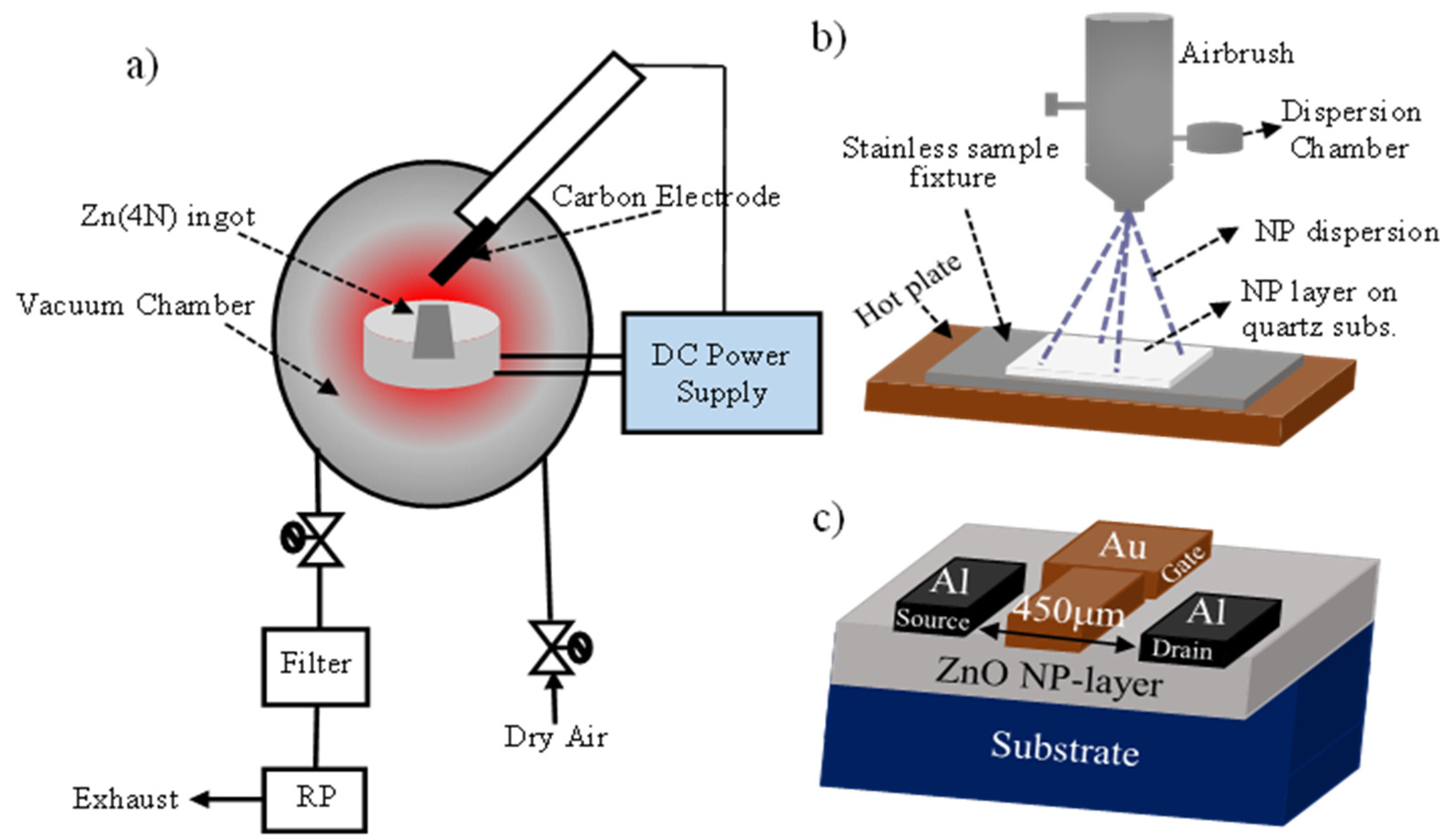
ZnO NPs were synthesized using an arc-discharge-mediated gas evaporation process. In the arc plasma method [
23], a commercially available zinc (4N) rod (metal Zn 99.99%, The Nilaco Corporation, Ginza, Tokyo, Japan) was used as the zinc source, and dry air was used as the oxygen source, while a carbon rod acted as the cathode. A schematic of the ZnO NP fabrication process is shown in
Figure 1a.
An arc current of 20 A was produced and a rotary vacuum pump (ULVAC KIKO Inc., Saito, Miyazaki, Japan) was used to maintain the pressure inside the chamber at approximately 610 Torr. Dry air was flown through the chamber at 5 L/min using a flow controller (KOFLOC (KOJIMA Instruments Inc.), Kyotanabe, Kyoto, Japan) (suppressing the nitrogen doping mode). This fabrication condition yielded the lowest N
2 concentration of approximately 0.01 (wt.%), whereas the condition with an arc current of 60 A yielded the highest N
2 concentration of approximately 0.31 wt.% [
24]. The aforementioned conditions (610 Torr, 20 A) were used to fabricate n-type ZnO NPs (designated as-prepared ZnO), which were the primary type of ZnO NPs used in this study. Ga-doping was carried out by mixing 0.2 g of ZnO NPs with 0.06 g of Ga
2O
3 NPs (Sigma-Aldrich Co. Ltd. 99.99% Purity) and annealing at 800 °C for 60 min in ambient air (high humid open air atmosphere) containing atmospheric N
2 and O
2, wet air, pure N
2, pure O
2, and dry air (designated “ZnO:Ga-open air”, “ZnO:Ga-wet air”, “ZnO:Ga-N
2”, “ZnO:Ga-O
2”, and “ZnO:Ga-dry air”, respectively). Here, wet air refers to air with a humidity of approximately 100% generated with water bubbling. Dispersions were prepared by dispersing 0.26 g of the aforementioned annealed NPs in 10 g of water using an ultrasonic homogenizer (Iida trading co., Ltd., Yao-shi, Osaka, Japan) (150 W, 3 min) with a frequency of 20 kHz, and then centrifuging them (3000 G, 1 min) to remove residual Ga
2O
3 NPs. This led to the successful removal of almost all of the residual Ga
2O
3 particles and the precipitation of large ZnO NPs. Then, 7 mL of the dispersion fluid was sprayed on a heated quartz substrate (hot plate temperature of 500 °C) at 5-s intervals for ~15 min. An airbrush spray coating method was used to sinter the NPs and avoid agglomeration. A schematic of this process is presented in
Figure 1b. Metal-semiconductor (MES)-gate type TFT structures using ZnO NP layers as channel layers were fabricated by Al evaporation (~50 nm) for the source (S) and drain (D) ohmic contacts, and by sputtering for the Au Schottky electrode (~30 nm) gate.
Figure 1c shows a schematic of the MESFET structure used in this study. Al/Au electrodes with a width and distance of 0.3 mm were constructed for the two-probe (
I–V) measurements. To determine the variation in sheet resistances and TFT performance,
I–V measurements were acquired using a shielding probe system and an E5270B precision measurement mainframe with an E5287A Atto-level high-resolution SMU module (Keysight Technologies, Santa Rosa, California, USA). The surface morphologies were observed using a field-emission scanning electron microscope (FESEM; JSM-7001FA, JEOL, 5 kV, Akishima, Tokyo, Japan) and scanning probe microscopy/dynamic force mode (SPM/DFM; SPM-9700, SHIMAZU). Powder X-ray diffraction (SmartLab, Rigaku Corporation, λ = 0.154 nm, Austin, TX, USA) was used to determine the crystallographic structure, whereas a Fluromax-4 spectrofluorometer (Horiba Advanced Techno Co. Ltd. Kisshoin Minami-Ku, Kyoto, Japan) was used to measure the photoluminescence (PL) with an excitation wavelength of 325 nm and exposure time of 0.2 s.
3. Results and Discussion
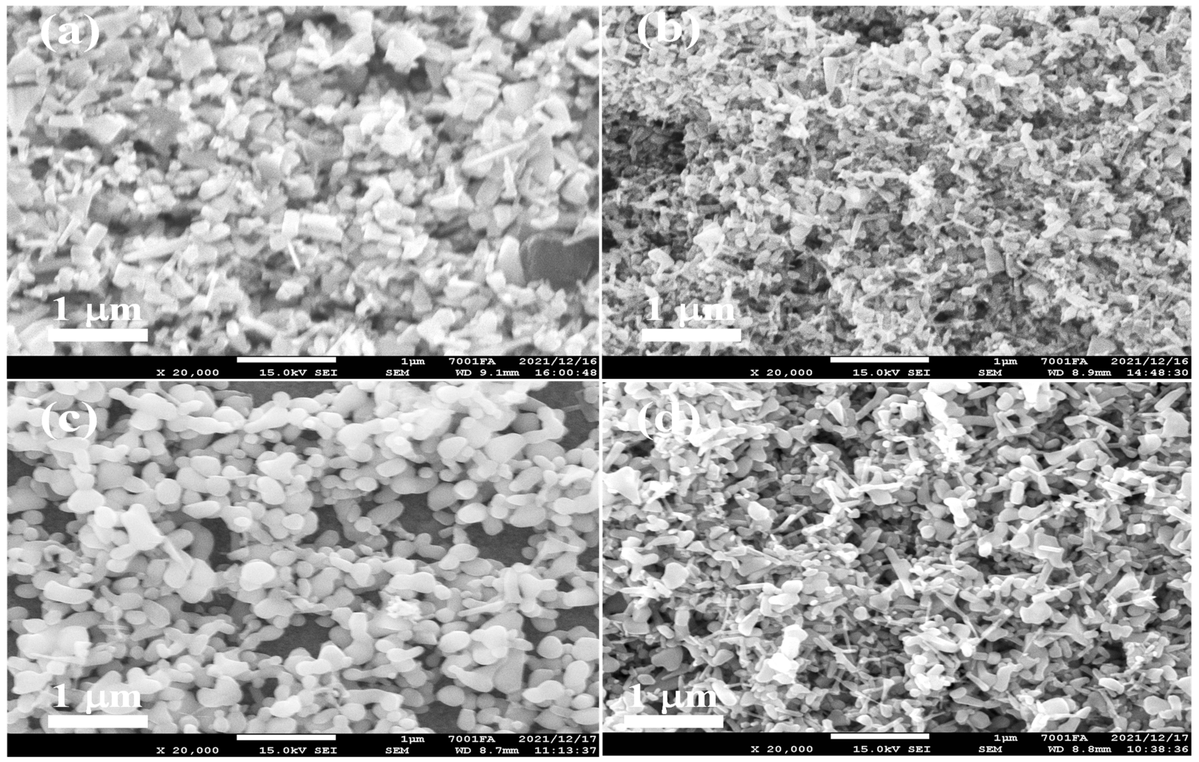
Scanning electron microscopy (SEM) was used to analyze the surface morphologies of the as-synthesized ZnO NPs (without centrifugal separation and before spraying), as-prepared ZnO, ZnO:Ga-open air, and ZnO-open air layers, which are shown in
Figure 2a–d, respectively. Here, “as-prepared ZnO” indicates ZnO NPs that had not undergone the Ga-doping process, and “ZnO-open air” indicates ZnO-NPs annealed in open air without Ga
2O
3 NPs, which is a reference sample for comparing only the effects of heat treatment. From
Figure 2a, it can be seen that the obtained ZnO NPs exhibited different morphologies in each NP; however, the basic shape was that of a hexagonal column. The surface morphology of the NP-layer with as-prepared ZnO (
Figure 2b) showed a higher density layer with smaller NPs due to the centrifugal separation process. After Ga-doping (
Figure 2c), the size of the particles became large as the small particles were fused, and the particles seemed to form a spherical shape due to the lowering of surface energy with Ga-diffusion. It was confirmed that performing only thermal treatment without Ga
2O
3 NPs caused only the enlargement of the particle size, while retaining the hexagonal column shape (
Figure 2d); therefore, the variation of shape shown in
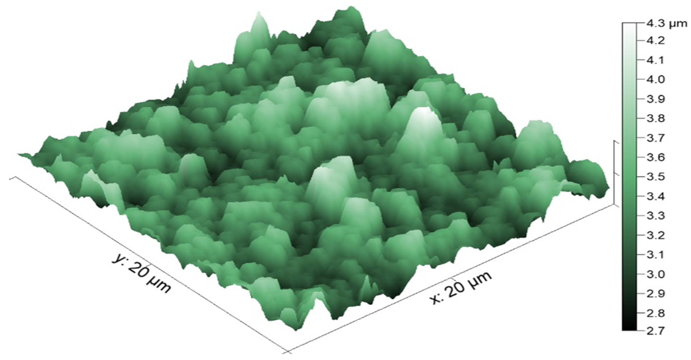
Figure 2c indicates the existence of Ga in ZnO NPs. Scanning probe microscopy/dynamic force mode (SPM/DFM) was used to confirm the surface roughness of the as-prepared ZnO sample (as shown in
Figure 3), yielding a surface roughness of 178 nm (20 µm × 20 µm measured area). The size of the NPs increased slightly after Ga-doping, which was attributed to the incorporation of smaller NPs during annealing at high temperatures. However, the variations were negligible (within 34 nm) compared to the original surface roughness, suggesting that the surface roughness of the other Ga-doped ZnO NP surfaces was comparable to that of the as-prepared ZnO.
The electrical properties of the ZnO layers were measured using a two-probe method. The sample was shielded from light by placing it in a shield box, and two probes were placed in contact with the Al/Au electrodes to evaluate the conductivity of the sample within a range of −10 V to 10 V. We used 0.3 mm × 0.3 mm square electrodes spaced 0.3 mm apart, so that the sheet resistance (
Rs) could be obtained from the slope of the
I–V curves, calculated using Equation (1).
where
RM is the measured resistivity,
W is the width, and
L is the distance. As for the two-probe (
I–V) measurement, the contact resistance is also a major issue in the achievement of relatively low resistivity. The contact resistance (2R
c) was estimated using the transfer length method (TLM) and the value was found to be about 140 Ω.
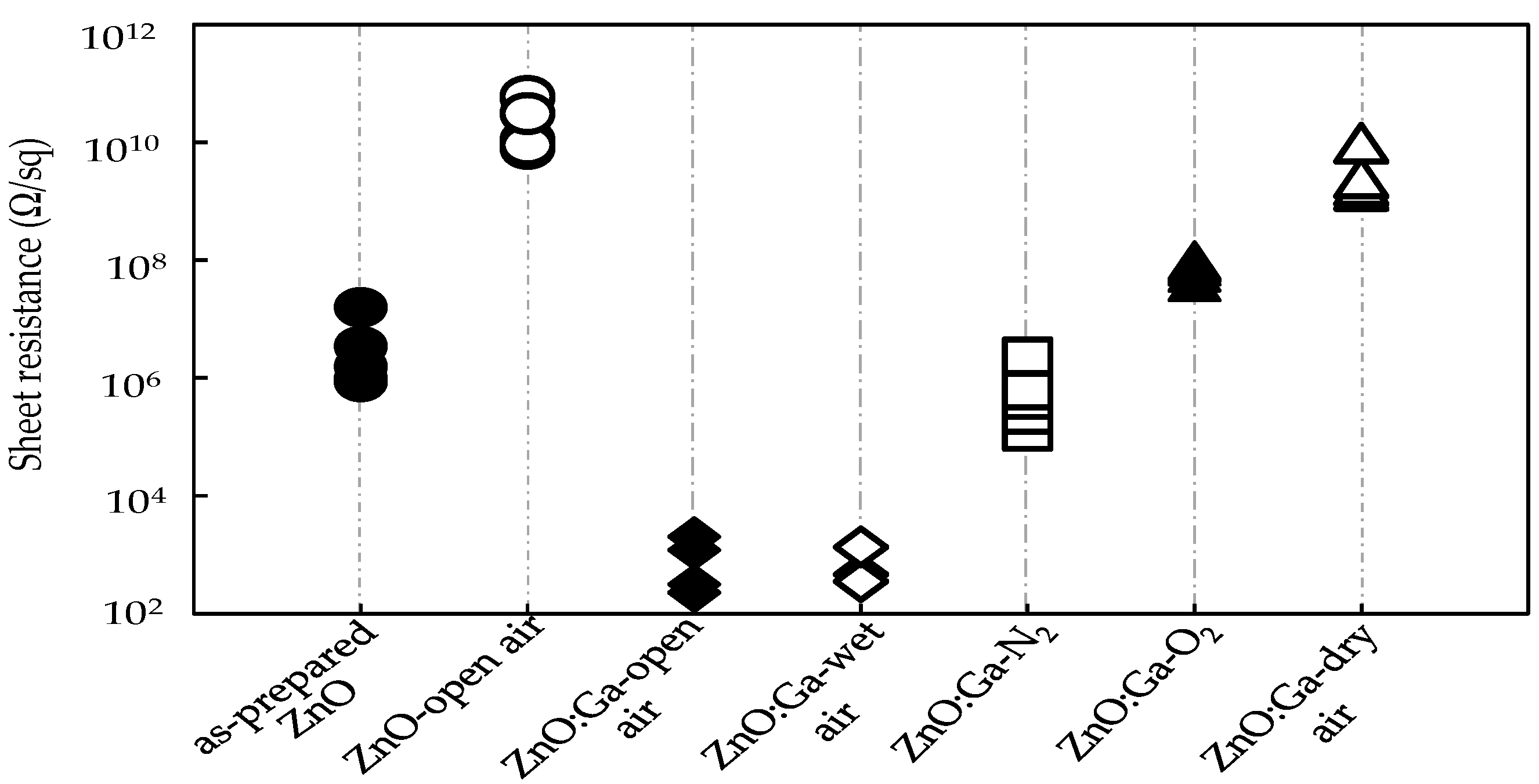
Figure 4 shows the distribution of sheet resistance values across different sprayed-NP layers. The average sheet resistances of each of the samples are summarized in
Table 1.
While several prior studies have demonstrated that the resistivity depends on the annealing temperature [
25], this study attempted to demonstrate that the resistivity induced by Ga-doping depends on the annealing atmosphere. The resistivity distribution graph clearly indicates that the lowest resistivity was obtained with ZnO:Ga-open air and ZnO:Ga-wet air layers. The high resistivity of the ZnO-open air layer was retained after thermal annealing without Ga diffusion, which can be explained generally by the reduction in electron carriers with the re-oxidation of oxygen vacancies. Here, compared to the resistivity of the ZnO-open air layer, all Ga-diffused samples showed a reduction in resistivity, and the properties of the ZnO particles were influenced by the thermal diffusion of Ga. Specifically, the resistance reduction for ZnO:Ga-open air and ZnO:Ga-wet air layers was significant, and the resistance reached the order of kΩ/sq, whereas the other three types of layers showed high resistivity. The ZnO:Ga-N
2 layer showed a relatively low resistance value compared to the ZnO-open air layer; however, this layer did not contain oxygen gas in the thermal process, i.e., re-oxidation of oxygen vacancy could not occur. Consequently, the resistance value of the ZnO:Ga-N
2 layer should be compared to that of the as-prepared ZnO. Therefore, as shown in
Figure 4, only the ZnO:Ga-open air and ZnO:Ga-wet air layers showed a substantial reduction in resistivity. The only plausible difference here is in the level of humidity present during the Ga thermal diffusion process.
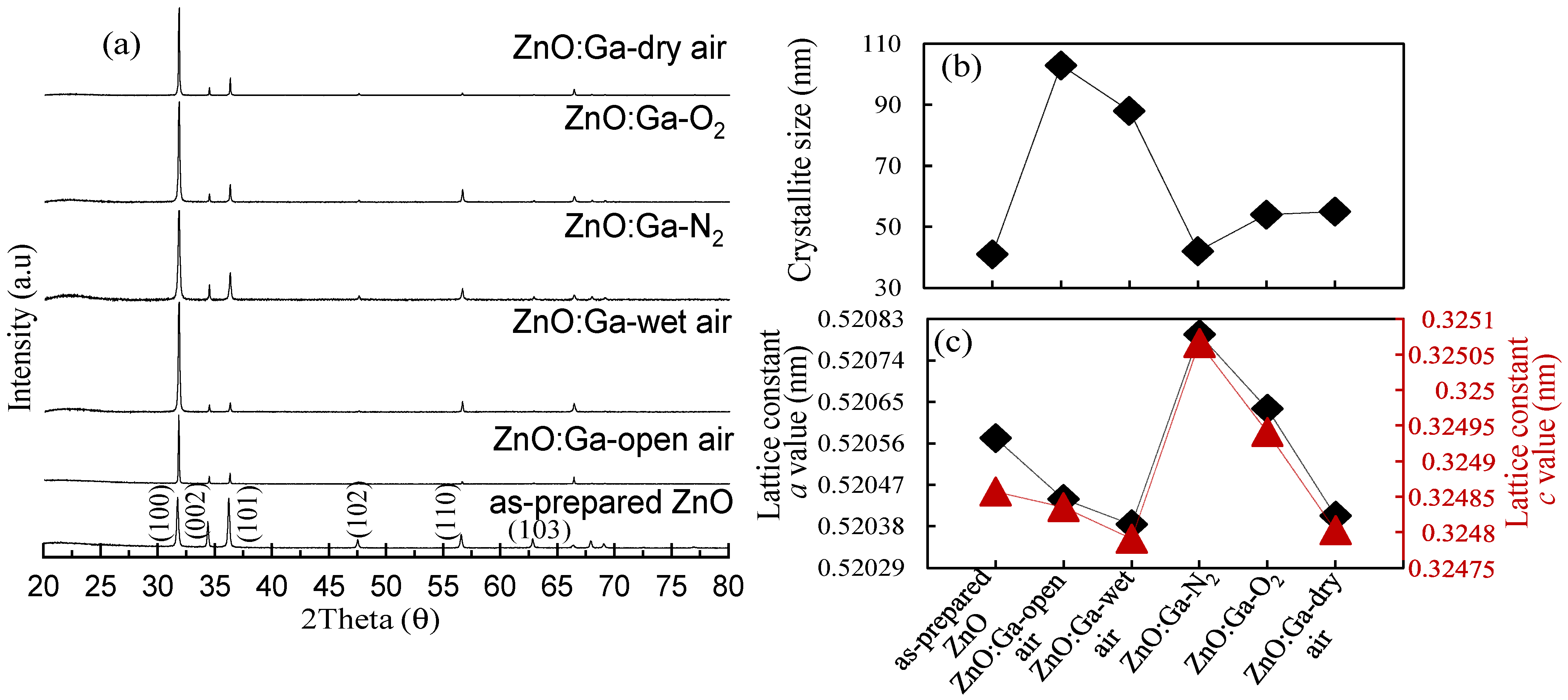
Figure 5a shows the X-ray diffraction (XRD) patterns of the as-prepared ZnO, ZnO:Ga-open air, ZnO:Ga-wet air, ZnO:Ga-N
2, ZnO:Ga-O
2, and ZnO:Ga-dry air layers. It can be seen that all the NPs had a hexagonal wurtzite crystal structure [
26,
27], matching well with the space group P63mc (No. 186, JCPDS No. 79-0208). Strong peaks at (100) and (101), along with a weaker peak at (002), were observed in all of the samples. The as-prepared ZnO layer had a high preferential orientation along the (100) plane. The crystalline dimensions of 2
θ along the
a-axis and the
c-axis were approximately 31.78° and 34.42°, respectively, for all of the samples. This indicates that the crystal structure of the sprayed layer was dependent on its thermal atmosphere, whereas the strong (100) peak indicated that the deposited layers had a preferred orientation with the
a-axis perpendicular to the substrate [
28]. The (002) peak position (34.414°) observed for all samples in this study was marginally lower than the corresponding value (34.467°) for bulk ZnO (COD 10 11 258) [
29], which in turn was owing to a deviation in the surface effects that caused lattice deformations and an increased lattice constant along the
c-axis [
30]. The thermally Ga-diffused NP samples exhibited a relatively high intensity, indicating improved crystallite growth and crystallinity. This was partly because, at this annealing temperature, Ga
3+ ions were incorporated into the ZnO matrix as substitutional impurities on the Zn lattice sites [
31].
The crystallite size (
D) of the sprayed layers was estimated from the FWHM values based on the (100) peaks using Scherrer’s formula, as shown in Equation (2) [
32], and the results are shown in
Figure 4b.
where
λ is the wavelength of the incident XRD,
β is the FWHM in radians, and
θ is the Bragg angle of the diffraction peak. The crystallite sizes of the samples are summarized in
Table 2.
The crystallite sizes of the Ga-doped NPs increased during annealing, particularly when annealing was performed in open air and in wet air. Owing to annealing, significant crystallite development in nanoparticles occurs because the atoms move to an inclinable position and then tend to combine with neighboring crystallites, resulting in the formation of large crystallites. Comparatively, the crystallite size of the annealed NP layer was larger than that of the as-prepared ZnO because of the smaller lattice distortion after annealing, which is attributed to the similarity between the atomic radii of Ga and Zn [
33]. Owing to the smaller crystallite size of the sprayed NP layer, the density of boundaries between the crystallites increased, leading to a higher resistivity of the conducting layer. After annealing, the crystallite size increased, resulting in a decrease in crystallite boundaries and reduced resistivity. Bragg’s law (2
dsinθ =
nλ) and the relationship formula (Equation (3)) were used to obtain the lattice constants
a and
c [
34].
where
dhkl is the interplanar spacing calculated from Bragg’s equation, and
h,
k, and
l are the Miller indices. The lattice parameters usually depend on many variables such as free-electron concentration, concentration of doping atoms, defects, the variation of ionic radii of the substituted matrix ion, external strains on the substrate, and temperature. The calculated lattice parameters for the as-prepared ZnO layer were found to be
a = 3.2485 Å and
c = 5.2057 Å, where the lattice constants range from 3.2475 to 3.2501 Å for the “
a” parameter and from 5.2042 to 5.2075 Å for the “
c” parameter [
35]. After thermal treatment and Ga-doping, these values varied with the temperature and atmospheric conditions. The calculated results for the lattice constant values in Å are shown in
Figure 5c. The lattice constant values of “
a” and “
c” showed a decreasing trend in ZnO:Ga-open air and ZnO:Ga-wet air layers compared to those in the as-prepared ZnO. The smaller ionic radii of Ga
3+ (0.62 Å) compared to that of Zn
2+ (0.74 Å) indicates that Ga atoms substitute Zn atoms effectively [
34]. Based on this consideration, the results also indicate that the ZnO:Ga-O
2 layer successfully achieved the Ga-doping effect; however, other factors such as the high density of crystallite boundaries analyzed from the XRD spectrum and the low crystallinity considered from the suppressed PL intensity described below degraded the current transporting ability in the ZnO:Ga-O
2 layer. Further investigation is required to clarify how these mechanisms reduced the lattice constant of the ZnO:Ga-O
2 layer.
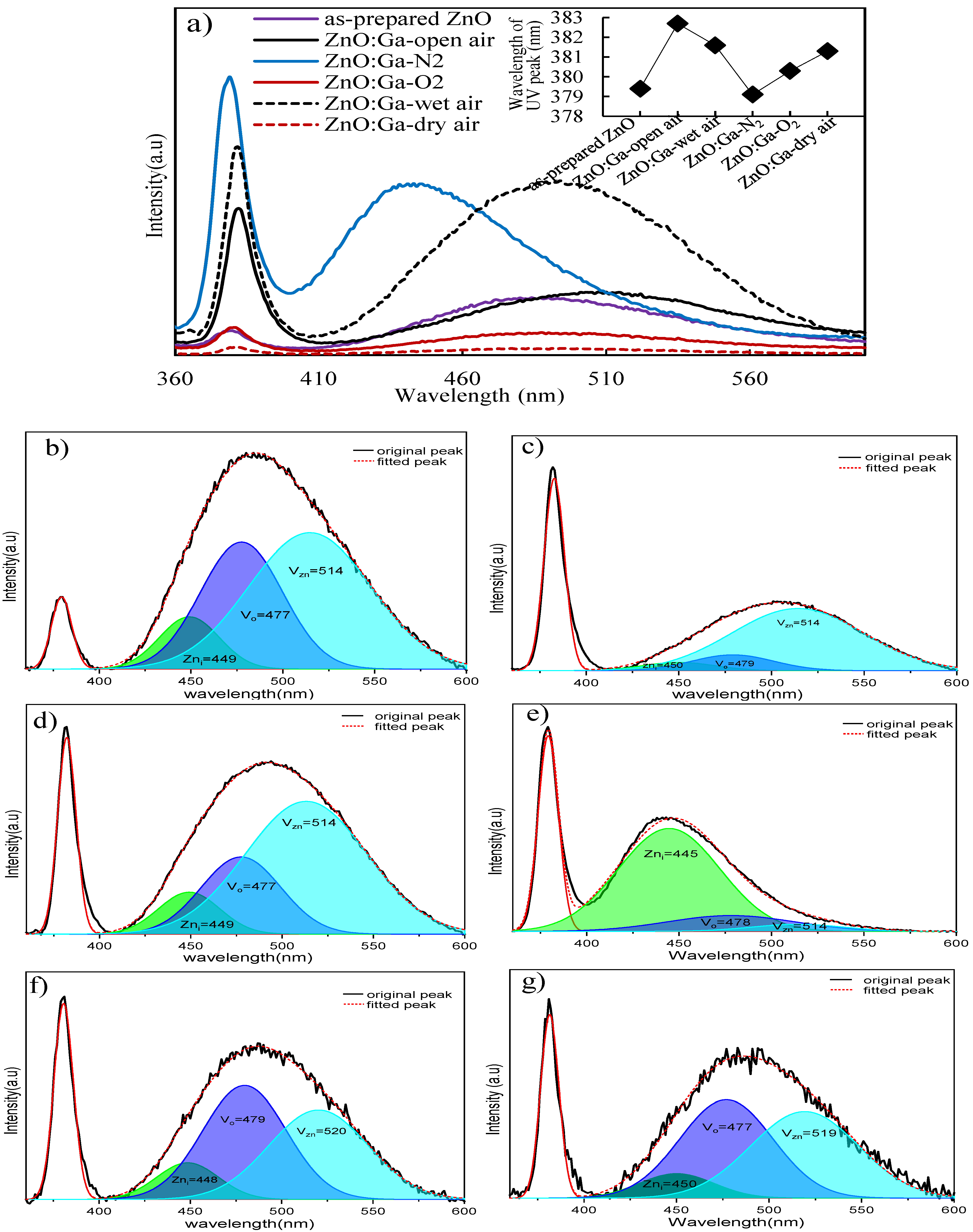
The PL spectra of the as-prepared ZnO, ZnO:Ga-open air, ZnO:Ga-N
2, ZnO:Ga-O
2, ZnO:Ga-wet air, and ZnO:Ga-dry air layers are comprised of ultraviolet (UV) emissions at a wavelength of 376–384 nm and a broad emission band in the visible range at 450–550 nm, which are shown in
Figure 6a. The variation of the UV peak positions is also shown in the inset of
Figure 6a. The enhanced UV emissions caused by the improvement of the crystalline and the red-shift phenomena caused by exciton and donor–acceptor (D–A) pair emissions were both observed in ZnO:Ga-open air and ZnO:Ga-wet air layers. These results could indicate an effective Ga-doping effect in these two samples, where a substantial reduction in the sheet resistance values was also observed, as summarized in
Table 1. For the ZnO:Ga-dry air layer, the UV peak position also showed red-shifting comparable to that for the ZnO:Ga-wet air layer, as shown in
Figure 6a; however, the luminescence intensity was small. This was caused by the existence of high-density non-radiative recombination levels such as surface defects of the NPs, which can possibly explain why the conductivity did not improve. The comparison of the surface state density of the NPs will be a topic of future research. To investigate the defect mechanism involved, the broad emission peaks were deconvoluted using the Gaussian function distribution, as shown in
Figure 6b–g. The number of native defects in numerous ZnO samples may vary among samples, as it largely depends on the particular history of each sample, e.g., the synthesis method and thermal treatment. In fact, under different conditions (e.g., n-/p-type doping, annealing temperature/atmosphere/pressure, and Zn/O-rich), the positions of the defect emission may change and may also combine several emissions. Based on the aforementioned considerations, we deconvoluted the PL spectra consisting of four sub-bands located at 382 (±3) nm for UV, 449 (±5) nm for Zn
i, 477 (±3) nm for V
O, and 514 (±6) nm for V
Zn [
36]. Although V
O is a deep donor, its formation energy is lower than that of Zn
i, which is a shallow donor in ZnO and, compared to all other native defects in n-type ZnO, V
Zn is considered to be the most significant deep level acceptor [
37]. Here, the ratio of V
Zn in the defect components was calculated as 81%, 65%, 5%, 43%, and 46% for ZnO:Ga-open air, ZnO:Ga-wet air, ZnO:Ga-N
2, ZnO:Ga-O
2, and ZnO:Ga-dry air, respectively. From these calculations, the ratios of V
Zn were found to be significantly larger in ZnO:Ga-open air and ZnO:Ga-wet air compared to those in the other three conditions. Several researchers have reported that the sublimation of Zn atoms occurred when the ZnO material was annealed at a high temperature (700–900 °C) in an ambient humid environment [
38,
39].
Clearly, there was humidity (H
2O) in the Ga diffusion process for the ZnO:Ga-open air and ZnO:Ga-wet air conditions; therefore, the sublimation of Zn atoms and the effective substitution of Ga atoms into the Zn sites could have occurred simultaneously. In contrast, although sufficient Ga diffusion occurred in the other three conditions [
22], Ga atoms could not be introduced into a suitable site, and the crystallites of ZnO NPs were degraded. Based on the XRD spectra in
Figure 5a, the peak height ratios of (002) and (101) to (100) for the ZnO:Ga-dry air, ZnO:Ga-O
2, and ZnO:Ga-N
2 layers differed from those of the ZnO:Ga-wet air and ZnO:Ga-open air layers. The details are not yet clear; however, one possible reason is that many diffused Ga atoms that could not substitute Zn sites prevented the coalescence of crystallites. Therefore, the ambient humidity may be one of the key conditions for the successful thermal diffusion of Ga atoms into ZnO NPs.
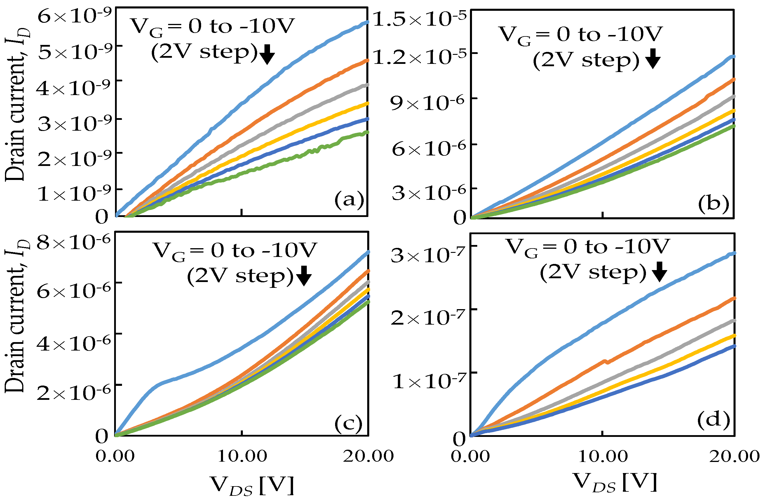
Here, the current controllability of TFT-based structure by the gate electric-field were confirmed in
Figure 7. Each TFT-based structure had a channel length of 450 μm and a gate width of 300 μm. The gate current of the MESFET exhibits behavior that is similar to that of a Schottky diode. The isolated work functions of the n-ZnO and gold (gate electrode) were in very close proximity at approximately 4.2 and 5.1 eV, resulting in the creation of a Schottky barrier along the channel [
40]. The Schottky barrier between the Au gate electrode and the ZnO NP layer was biased in the opposite direction for negative gate voltages, and the gate current was approximately equal to the voltage-independent saturation current of the Schottky junction. In a MESFET device, the density of free charge carriers (and therefore, the conductivity of the semiconductor) is determined by the depletion width of the Schottky contact between the metal gate electrode and the semiconductor [
41].
Figure 7a–d shows the
ID–
VDS characteristics of the fabricated TFT-based structures whose channels were made of as-prepared ZnO, ZnO:Ga-open air, ZnO:Ga-N
2, and ZnO:Ga-O
2 layers, respectively. For all cases, the gate leakage current was confirmed to be sufficiently low, on the order of 10
−14 A. The
ID–
VDS results imply that, by using Ga-doped ZnO NP layers (especially in ZnO:Ga-open air), the drain current is increased by at least 1000 times or more compared with the as-prepared samples. The decrease in the drain current observed in ZnO:Ga-N
2 (10
−6) and ZnO:Ga-O
2(10
−7) is consistent with the resistivity behavior graph (shown in
Figure 4). This suggests that the doped Ga atoms in the ZnO NPs act as activated donors and generate carriers, effectively reducing the channel resistance. In addition, clear electric field effects were also observed by varying the applied gate voltage (V
G) for all cases.
When the gate voltage is zero (VG = 0 V), the highest drain current is observed, indicating that the device is typically ON. Furthermore, after applying the negative gate voltage (−VG), the drain current decreases gradually, causing the depletion region to increase and inhibit the electron flow in the conduction layer. If the gate voltage is sufficiently negative, the device will turn OFF. These results strongly indicate the possibility of realizing TFT devices using our Ga-doped ZnO NP layers.


