Article

Ecofriendly Water-Based Solution Processing: Preliminary Studies of Zn-ZrO2 Thin Films for Microelectronics Applications

1
Department of Physics, University of the Punjab, New Campus Lahore, Lahore 54590, Pakistan
2
Centre for Solid State Physics, University of the Punjab, New Campus Lahore, Lahore 54590, Pakistan
3
Centre for Micro and Nano Devices, Department of Physics, COMSATS University, Park Road Campus, Islamabad 45550, Pakistan
*
Author to whom correspondence should be addressed.
Coatings 2021, 11(8), 901; https://doi.org/10.3390/coatings11080901
Submission received: 14 July 2021 / Revised: 25 July 2021 / Accepted: 27 July 2021 / Published: 28 July 2021

Abstract

:
This paper demonstrates the high yield and cost effectiveness of a simple and ecofriendly water-based solution processing, to produce Zinc-doped Zirconia (Zn-ZrO2) composite thin films, onto glass substrates, with excellent optical properties that make them of great interest for optical and microelectronics technologies. The effect of Zn variation (given as 10, 15, 20 at.%) on the crystallization, microstructure, and optical properties of ZrO2 film was examined. The addition of Zn did not restructure the ZrO2 lattice, as the results indicated by X-ray diffraction (XRD) and Raman spectroscopy revealed neither any mixed or individual phases; rather, all the films retained the amorphousness. Nonetheless, Zn did control the grain formation at the film surfaces, thereby changing the surface morphology. Atomic force microscopy (AFM) and scanning electron microscopy (SEM) evidenced homogeneous, compact, crack-free, and dense films with surface roughness below 2 nm indicating smooth surfaces. The films were highly transparent (>80%) with tunable optical band gap Eg (5.21 to 4.66 eV) influenced by Zn dopant. Optical constants such as refractive index (n), extinction coefficient (k), and dielectric constant (ε) were obtained from spectroscopic ellipsometry (SE), and a correlation was established with respect to the doping level. A high value of n > 2 value indicated high packing density in these films, and it decreased slightly from 2.98 to 2.60 (at 632 nm); whereas, optical losses were brought down with increasing Zn indicated by decreasing k values. The photoluminescence (PL) spectra showed UV emissions more pronounced than the blue emissions indicating good structural quality of all the films. Nonetheless, added defects from Zn had suppressed the PL emission. The technique presented in this work, thus, manifests as high performance and robust and has the potential comparable to the sophisticated counter techniques. Furthermore, the Zn-ZrO2 films are promising for a low-cost solution to processed microelectronics and optical technologies after reaching high performance targets with regards to the electrical properties.

1. Introduction

The advent of modern transparent technology is owed to the development of metal oxide-based materials, especially semiconductors. The transparent metal oxides proffer the future prospect of low-cost microelectronics [1] and the next-generation optical displays [2,3,4] with improved characteristics such as high (>80%) transparency (due to their wide optical bandgap > 3 eV in general), large carrier mobilities, and ease of processing. Zirconia (ZrO2) is not only a wide band gap (3–7.8 eV) [5,6] and highly stable metal oxide, but it exhibits larger values of both refractive index and dielectric constant that make it aptly suitable for a great range of applications. The latter includes transistors [7,8], bio medical applications [9], sensors [10,11,12], and catalysts [13], just to name a few. Doping of ZrO2 with various materials has attracted a great deal of attention for an improved end product as compared to the pure oxide, since the former can strongly influence physical, chemical, and electronic properties producing high performance for multiple applications. ZnO doping into ZrO2 has emerged, fairly recently, as an interesting approach for customized properties and has made its ground by showing remarkable characteristics especially for sensing [12] and photocatalytic activity [6]. Among the various advantages associated with using ZnO, the most important include easy processing, wide band gap with large exciton binding energy 60 meV [14], and exceptionally high photo- and chemical stability [15]. In the following paragraph, we have given a very brief overview of previous work done on Zn-ZrO2 material system.
Nanostructure thin films of ZnO-ZrO2 fabricated by the sol gel method with molar concentration of Zn varied up to 75% [16,17,18,19] showed an improvement in microstructure, in transmittance, and in both catalytic and antibacterial activity. Interestingly, ZnO hexagonal phase could mark its appearance only after 25 mol.% of ZnO content [17,20], although a decrease in band gap and an increase in crystallite size were observed, with increasing ZnO doping level. Additionally, ZnO-ZrO2 nanoparticles [6] obtained by the impregnation method resulted in optimal photocatalytic activity for 50 wt.% of the ZnO doping level. In addition to the solution processing, vacuum-based techniques such as DC magnetron sputtering have also been employed to make thin films of the ZrO2-ZnO [12] with the purpose of investigating characteristics for humidity sensing. The nano-sized grains in these films (confirmed from SEM) were found to be the likely cause in decreasing the resistance. Most of these reports have focused mainly on sensing/catalytic applications of this material system fabricated by sol gel method using organic precursors. It is known that despite the high outturn and cost effectiveness of the solution processing, the films, thus, produced are rough, cracked, and porous [21]. These are mainly the consequence of decomposition of organic species. Additionally, the wet gel after being dried and the precipitation that occurs in sol formation, in the sol gel method, lead to voids in the films and makes the procedure very cumbersome. Adding further, and most importantly, the solution processing method results in a chemical waste that becomes noxious for the environment. To address and rectify these issues, the research interest has, therefore, shifted to a new paradigm of water-based solution processing [22], employed earlier for ZnO-based transistor applications using inkjet printing. It is quite recent that our group has successfully developed ecofriendly water-based solution processing, which need not rely on sol gel preparation to fabricate oxide-based thin films [23,24]. The same methodology has been applied in this report. Since water-based solution processing is an ecofriendly and risk free deposition route, the technology will open new horizons for next-generation transparent microelectronic technologies.
In this work, applying traditional spin coating of a simple and quickly made water-based solution, we have fabricated Zn-doped ZrO2 films and have emphasized on the understanding of the effect of doping level on the films’ properties. The films were characterized for structure and morphology by X-ray diffraction (XRD), Raman spectroscopy, atomic force microscopy (AFM), and scanning electron microscopy (SEM) and for optical properties by ultraviolet-visible spectroscopy (UV-Vis), spectroscopic ellipsometry (SE), and photoluminescence (PL). The current study probes how Zn is incorporated in the ZrO2 lattice, investigates the doping effect on the surface morphology, grain architecture, and structural phase, and finally, inspects the reason for the decrease in optical band gap energy, change in the optical constants, and luminescence after doping. It is important to mention that previous reports on Zn-ZrO2 films do not cover all of these topics, rather investigate from the perspective of catalytic applications more; therefore, the present study is presumably not a buildup on the previous studies.

2. Experimental Details

2.1. Materials and Thin Film Deposition

The following precursors were used in this study, bought in analytical grade purity from Sigma Aldrich: Zirconium oxychloride octa hydrate (ZrOCl2·8H2O) and Zinc nitrate hexahydrate (Zn(NO3)2·6H2O). Both host (Zr-based) and doped (Zn-based) solutions (0.3 M concentration, each) were prepared separately using deionized (DI) water without any catalytic agents. Transparent, homogenous, and stable solutions were ready after stirring for 1 h at room temperature. Four different solutions were prepared with Zn doping level varied as 0, 10, 15, and 20 at.%. All solutions were filtered through 0.22 μm PTFE syringe filters just prior to spin coating. For synthesis, the 2 × 2 cm2 microscopic glass substrates were ultrasonically cleaned first in acetone and then in IPA for 30 min at 60 °C each time and, finally, rinsed with DI water again before being dried off with a nitrogen gun.
The films deposition was carried out by spin coating method using SÜSS Micro Tec Lithography GmbH spin coater (Garching, Germany). The procedure comprised three cycles of solution coating and a final round of thermal annealing. In each cycle, the solution was dispensed onto the glass substrate followed by spin coating at 500 rpm for 6 s and then at 2000 rpm for 25 s and baking at 200 °C for 10 min in air. After three cycles, thermal annealing at 350 °C of the synthesized film was carried out for 1 h in air. The entire procedure was very simple and quick. Films, thus, fabricated were used for all subsequent analysis, whereas different samples were identified with the following scheme. The pristine and Zn (10, 15, and 20 at.%)-ZrO2 films are referred to as ZrO2, ZrZ10, ZrZ15, and ZrZ20, respectively.

2.2. Characterization and Data Analysis

The structural phase was determined from X-ray diffraction (XRD) patterns obtained using STOE Powder Diffraction System (Bruker D8 machine, Billerica, MA, USA) using Cu Kα radiation and from Raman Spectra acquired using a RamBoss Raman Spectrometer (DongWoo Optron, Gwangju-si, Korea) equipped with an argon ion laser (λ = 514 nm), in a back-scattering configuration. For XRD patterns, the detector used was a scintillation counter, and the range of 2θ was from 20.000° to 80.000° with a step size of 0.040° and an exposure of 1.5 s per step. XRD and Raman spectra for all the samples were studied using Origin (Pro), Version 2018. OriginLab® Corporation, Northampton, MA, USA. The surface topography and microstructure were analyzed by atomic force microscopy (AFM) using Agilent Technologies microscope (Santa Clara, CA, USA) and scanning electron microscope (SEM) (JSM-6490A, JEOL, Tokyo, Japan) at 10 kV accelerating voltage. Prior to SEM studies, each sample surface was covered with a thin layer of gold deposited via sputtering. AFM images were obtained from 5 × 5 µm2 area of each sample using tapping mode; surface morphology and root mean square (RMS) roughness were estimated using the Gwydion software. The optical properties of the films were assessed by UV-Vis transmission using BMS 2600 spectrophotometer (New York, NY, USA), the spectroscopic ellipsometry using Sentech instrument GmBH 850 (Berlin, Germany) fitted with Xenon lamp (incident at 70°) and by photoluminescence (PL) using RamBoss spectrometer (DongWoo Optron, Gwangju-si, Korea) fitted with argon ion laser (325 nm). The absorption coefficient (α) was determined using transmission spectra; the band gap energy Eg values were evaluated, using Tauc method, from x-intercept of the (αE)2-E graph for all thin film samples. Urbach energy Eu quantifying absorption edge tailing into the band gap was evaluated from a plot between ln(α) and E. Film thickness (t), refractive index (n), extinction coefficient (k), and dielectric constant (ε) for all the samples were determined from ellipsometry data. The PL spectroscopy was performed at −50 °C, with an exposure of 1 s for each reading, and the spectra were detector response subtracted and fitted with Lorentzian distribution to obtain the desired information, using Origin software 2018 64 bit.

3. Results and Discussions

3.1. Structure and Surface Morphology Studies
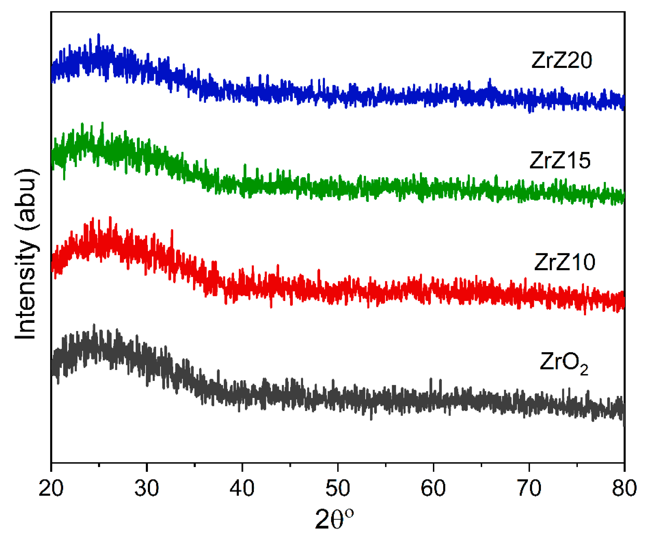
3.1.1. XRD Studies

To identify the crystalline phase in water-based solution processed ZrO2 film and the changes induced by the Zn doping, XRD was performed. Figure 1 shows the XRD patterns obtained for ZrO2, ZrZ10, ZrZ15, and ZrZ20 thin film samples.
The absence of any peaks in the spectrum, for ZrO2 film, indicate that there is no crystalline phase present in the film. Especially, the lack of distinct peaks between 28°–32° clearly indicates the lack of tetragonal (t-) and monoclinic (m-) phases [25]. The presence of a broad peak/hump near 25° confirms that the film is amorphous. This is in agreement with a recently published report about Zn-doped ZrO2 nanoparticles [19], whereby the amorphous phase has been observed for low concentration of Zn (0.25–1 at.%). It is important to mention that the amorphous phase observed in this study is attributed to the annealing temperature chosen while depositing these films. It is known that pristine ZrO2 thin films exhibit an amorphous structure when processed under 350 °C of temperature [26]. Furthermore, the result produced in the present study accord with the non-crystalline phase observed in ZrO2 after annealing at temperatures of 350 °C [27]. Lin et al. [28] had observed crystalline phase for temperatures reaching around 450 °C and above.
In Figure 1, the spectra for the doped samples (ZrZ10, ZrZ15, ZrZ20) exhibiting protuberance similar to that of the pristine ZrO2 thin film clearly indicate that the baseline structure is not affected by the added dopant. Moreover, no diffraction peaks are, furthermore, observed in the spectra that can correspond to the characteristics ZnO structure, which suggest that the dopant was well dispersed in the matrix of ZrO2 and could not establish itself in the form of ZnO. However, it is known that solution processing can induce a large number of vacancies (o) and interstitials (i); therefore, we expect that both Zr(i) and Zr(o) would modify the Zr–O bond length. Moreover, Zr(o) antisites would have Zn ions surrounded by them. Both these cases will result in high structural disorders leading to amorphousness in these films [29]. The result also agrees with a previous finding [17], which shows that incorporation of Zn in fact inhibits crystalline phase of ZrO2. Furthermore, it is also anticipated that the lack of distinctive ZnO peaks could be the effect of Zn on ZrO2 in a way that Zn-ZrO2 films reduce the crystallite size and keep the d-spacing within the range of pristine ZrO2, which is why it has no noticeable effects on the deposited film. The results presented here are in agreement with those obtained from sol gel derived ZnO-ZrO2 films fabricated at 400 °C, with 1:1 molar ratio [30] and ZnO-ZrO2 nanoparticles [31]. The previous study [30] revealed absence of any mixed/or individual oxide phases, while the films were more of amorphous phase. Nonetheless, increased annealing temperature (750 °C) provoked better crystallization corresponding to both ZnO and ZrO2. Therefore, keeping in view the previous reports and the results obtained here, we speculate that increase in annealing temperature and dopant concentration can ultimately show the crystallites of ZnO in the matrix [32]. As the argument related to dopant concentration is supported by a recent finding [17], whereby the well-defined peak representing the ZnO phase in ZnO-ZrO2 nanocomposites were observed only when Zn concentration level reached to 25 mol.%. Therefore, the results obtained in the present study reinforce the previous finding that low doping level does not make ZnO visible in ZrO2.

3.1.2. Raman Spectroscopy Studies

The XRD patterns shown in Figure 1, although they give clear evidence of the amorphous phase in the deposited ZrO2 films, irrespective of the doping concentration of Zn but to elucidate the structural changes induced by Zn doping in ZrO2 films further, Raman spectra were obtained and analyzed. Before proceeding, it is to be noted that crystalline phases of ZrO2 can be identified with specific phonon modes designated by bands/peaks in the observed Raman spectrum. For example, Raman spectrum for t-ZrO2 would exhibit phonon bands at 150, 260, 465, 640 cm1 [33] and for m-ZrO2, at 180, 190, 335, 380, 475, 635 cm1 [33]; there are even more bands that can be present. However, for ZrO2 in amorphous form, these specific phonon modes rather than appearing as peaks/bands would smear away and appear more similar to a continuum as a result of structural disorders [34] and, hence, would characterize the film as amorphous.
In order to draw a link between changes observed in Raman spectra due to doping, each spectrum is background subtracted. Raman spectra obtained for all the samples are shown in Figure 2. In the first glance, Raman spectra look similar. However, there were two characteristic differences observed in the Raman spectra from Zn-ZrO2 films; the Raman spectrum shows a peak/hump at around 560 cm1, which is completely absent in pure ZrO2 films. Secondly, the hump in pure ZrO2 film observed at 450 cm1 is suppressed by a 560 cm1 hump. The spectrum of pristine ZrO2 thin film sample appears to be a continuous band, with an absolute absence of distinct ZrO2 phonon peaks, throughout the given Raman shift spanning across 100–1000 cm−1. This clearly stipulates the characteristic feature of Raman spectrum identified as of an amorphous phase. Furthermore, it is clear from Figure 2 that Raman spectra for all the doped samples again represent a rather broad band, which does not alter as the doping level of Zn is changed. This result seconds our XRD result presented above and reinforces that Zn-ZrO2 films maintain the amorphous phase. These Raman results are also comparable to an earlier finding [17], whereby Raman spectra for the ZnO-ZrO2 nanoparticles show an absence of ZnO peaks and a broadening of ZrO2 peaks as the ZnO content is increased. This possibly confirms that Zn inhibit the crystalline phase and increase the structural disorder. In the present study, however, it is very interesting to know that Raman spectra representing the Zn-ZrO2 films (Figure 2) show the phonon mode at 562 cm−1, which is known as A1 (LO) mode. The latter is one of the characteristics phonon modes used to identify the crystalline phase (wurtzite) of ZnO [35] including E2(high), A1 (LO), and E1 (LO), etc. [24].
The effect of increased concentration of Zn in ZrO2 films is also indicated by the shift observed in the A1 (LO) mode, as shown in Figure 2 and Table 1. Furthermore, to our interest is full-width at half maximum (FWHM) of A1 (LO) mode, which is considered as a measure of disorder/damage in the crystal [36]. It has been found to increase from 114.98 ± 19.40 to 312.80 ± 71.25 cm−1 as the Zn doping level is increased, see Table 1. It is interesting to note from Table 1 that FWHM is reduced for the sample ZrZ15 indicating that 15 at.% is the optimal amount of Zn content, which leads to reduce the defects and, hence, disorder in the host film of ZrO2. This is contrary to the 20 at.% of Zn (sample ZrZ20) that has caused an enhancement in the disorder significantly by adding more defects in ZrO2 film.
These investigations clearly lead to the finding that all the ZrO2-based films (pristine and Zn-doped) have an amorphous phase in common; however, Zn has marked its presence without bringing a clear change in the nature of underlying structural phase. Although not a significant effect of Zn on Raman spectra of doped samples is evident, but increasing disorder can be attributed to surface defects such as oxygen vacancies [31], as shown in the optical studies given below. No trace of crystallization with the added dopant has been observed, although an increased amount of dopant may lead to change in the phase structure as evidenced from previous report [17].

3.1.3. AFM Studies

To investigate the effect of Zn doping on surface morphology of ZrO2 films, AFM images were used to examine grain growth and surface roughness. Figure 3a–d shows 3D AFM images, for all the samples of ZrO2, whereby the change in surface morphology can be clearly seen. The simple water-based solution processing used in this work is found to produce dense, crack-free, and smooth film for each sample. The grain growth and a minimal increase in already low surface roughness values are the outcome of Zn doping into ZrO2 films.
It can be seen from Figure 3a that ZrO2 thin film shows a noticeable lack of undulations indicating a rather smooth film surface having good adhesion to the substrate. However, as the Zn dopant is added, we can observe from Figure 3b that the homogeneous surface now has grains that are distributed all over the area. A further increase in the doping level (Figure 3c,d) influences the grain growth strongly, as can be seen for ZrZ20 film, where larger and fewer grain islands dispersed rather periodically in the matrix are evident. However, an intermediate level of doping (Figure 3c) demonstrates a rather analogous surface morphology to that of the pristine ZrO2 (Figure 3a) except for fewer grains added. Quantitative analysis of these images validates these findings, as found from the observed trend in the grain size as well as in surface roughness of ZrO2 films with an increasing doping level. The information is listed in Table 1, which represents an overall increase in grain size, given as 23.25, 15.50, and 38.09 nm for ZrZ10, ZrZ15, and ZrZ20 samples, respectively.
The mean roughness (Ra) and root mean square roughness (Rq), indicators of the surface deviations/imperfections from the median plane found from AFM image of each sample, are listed in Table 1. On the length scale of 5 × 5 µm2, the surface roughness value, for each sample, is of the order of ≤2 nm, which is a relatively low surface roughness indicating rather smooth film and is comparable to those obtained for ZrO2 films fabricated by sputtering [37]. This again adds to the aptness of this low-cost water-based solution processing and makes it a robust and reliable method for future technologies. Moreover, with the added dopant, the ZrO2 films exhibit nominal increase in the roughness values, as shown in Table 1. This trivial change is attributed to the minor decrease in density of nucleation centers and to the grain’s configuration [38], as the doping concentration is varied in ZrO2 films. It is important to mention that the surface roughness of the gate dielectric used in devices plays an important role to achieve high mobilities [39] by reducing the carrier scattering. Moreover, a smooth surface is useful for current stability in a transistor operation leading to high on–off current ratios. Therefore, a lower surface roughness value obtained in this study makes ZrO2 film more promising as a dielectric candidate to attain high performances for low-cost, ecofriendly device applications.

3.1.4. SEM Studies

To confirm a smooth and crack-free surface morphology in ZrO2 film at different doping levels of Zn, the samples were further characterized by SEM. Low-magnification (×10,000) SEM images for all the samples are shown in Figure 4a–d. They reveal that all the film samples are uniformly deposited onto the glass substrates. Moreover, all the films are macroscopically flat and free of voids and cracks, which again complements to the AFM results and also approve the appropriateness of this low-cost water-based solution processing method for large area production.
Figure 4a shows a ZrO2 film sample, which represents highly homogeneous, dense, and a mostly flat surface with no surface imperfections. From Figure 4b–d, it can be seen that Zn-ZrO2 films are homogeneous with grains that are dispersed non-uniformly and that grow in number, as the doping level is increased. These results are in agreement with the AFM studies.
Summarizing the structural data, it must be noted that after adding Zn to ZrO2 (in 0, 10, 15, and 20 at.% concentrations), the films maintain the amorphous phase, although ZnO inhibits the formation of any structural phase and adds more disorder to the Zn-ZrO2 films. Surface of all of the film samples is dense, showing an absence of any defects (voids/cracks); the roughness of the films is incredibly low, although it increases slightly with an increase in Zn concentration. The result proves their excellent performance for low-cost and ecofriendly device applications.

3.2. Optical Properties

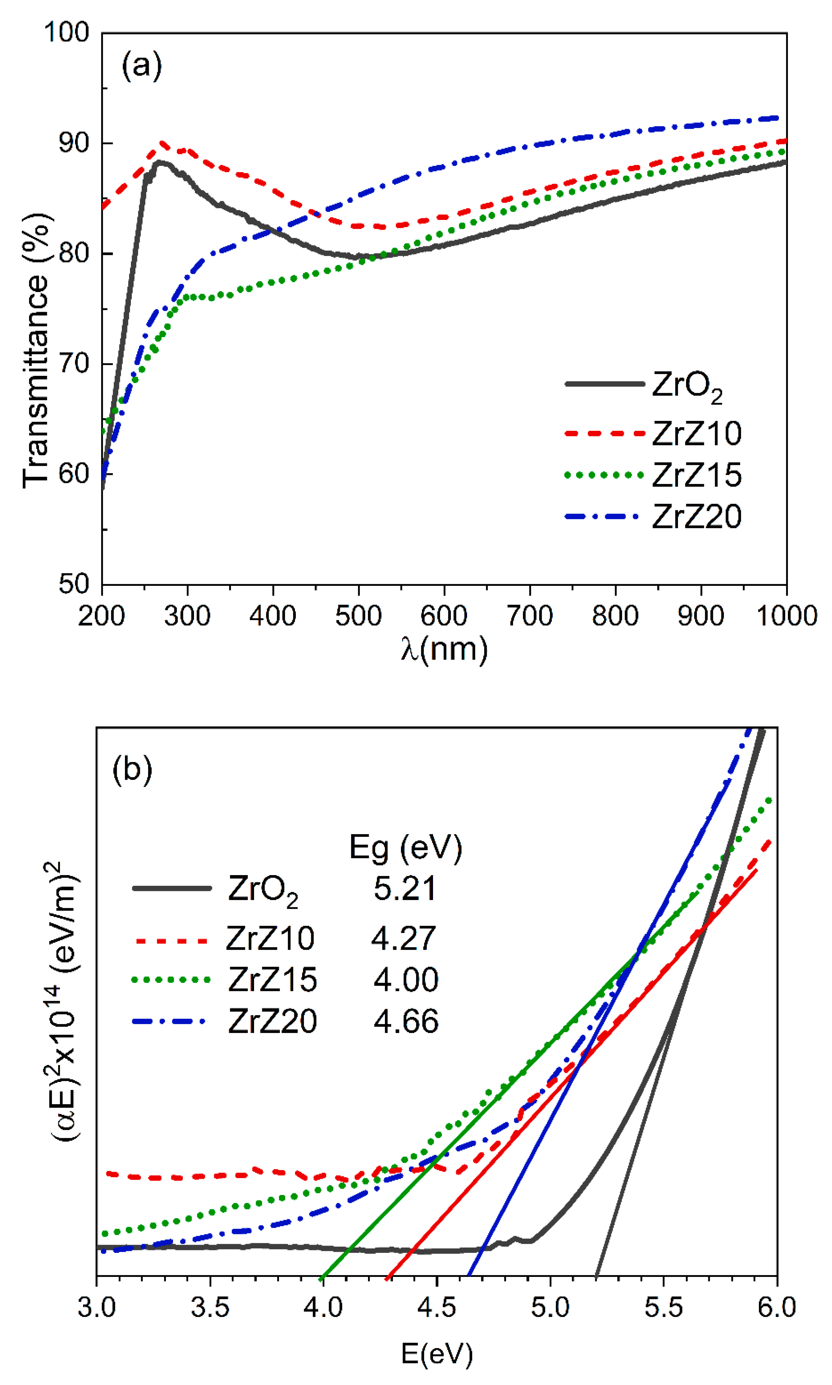
3.2.1. UV-Vis Optical Transmittance Analysis

The optical transmittance (T) spectra of Zn-ZrO2 thin film samples measured across the spectral regime (200–1000 nm) revealed highly transparent films with average percent transmittance ≥ 81%, as shown in Figure 5a, demonstrating that the films produced are suitable for transparent technologies. All the films clearly exhibit a complete and uninterrupted transmittance (T), with no sign of fringes, across the measured spectral region. This indicates that films are not only thin but are potential candidates for optical applications for being able to transmit the major portion of the incident light. The transmittance calculated over the entire wavelength region for all the samples is given in Table 2, and we can notice that Zn doping in ZrO2 films actually do not affect the transmittance adversely. However, it changes nominally such that it increases for samples ZrZ10 (86%) and ZrZ20 (85%) but decreases for the sample ZrZ15 (81%) when compared with pristine ZrO2 film (83%). We expect the phenomenon is more likely an interplay of scattering from surface defects and from grain boundaries. A relatively smoother surface and regular grain boundaries as obtained for the samples in the present case normally lead to enhanced transmittance. Nonetheless, defects induced by both added dopant and by the deposition environment, which was air in this case, can increase the surface scattering, thereby decreasing the transmittance. Based on these arguments and the increase and decrease observed in transmittance for Zn-ZrO2 samples, we speculate that an uncontrolled deposition environment does not allow us to establish a clear relationship between doping level and transmittance.
The fundamental absorption edge is found to be near the UV region, for all the samples, where the optical transmittance drops, and since it is within 220 nm, therefore, it allows these films to be used as UV-filters. As the doping level is varied, a red shift in the absorption edge is observed, which also identifies the corresponding decrease in the band gap energy (Eg). The direct band gap energy (Eg) values, listed in Table 2, were assessed using the well-known Tauc method by extrapolating the linear segment of the (αE)2 versus the E curve for each sample, as shown in Figure 5b. The absorption coefficient (α) was calculated from the following expression, for each sample.
α = 1 t ln 1 T
Here, t represents the film thickness, which was evaluated from spectroscopic ellipsometry measurements and has been given for each sample in Table 2. From this investigation, we have observed that pristine ZrO2 film sample exhibit Eg = 5.21 eV, which clearly falls in the wide-band gap materials’ range (3–7 eV). Hojabri et al. [40] reported that magnetron sputtered ZrO2 film in amorphous phase exhibited a band gap of 5.34 eV. Ibrahim et al. [6] recently reported Eg = (3.16, 4.61 eV) value for pure ZrO2 thin films fabricated via impregnation method. The Eg value for pristine ZrO2 films obtained in this work using a simple water-based solution processing is, therefore, comparable to the previously reported value acquired for ZrO2 films fabricated via techniques better known as futuristic and intricate.
In case of Zn-ZrO2 films, we observe a decrease in Eg value down to 4.66 eV acquired for the maximum level of doping (sample ZrZ20), as shown in the Figure 5b. It has been established that crystal order/disorder and defects [41] play a strong role in the electronic structure of ZrO2, which can change the Eg. The observed decrease in Eg, in this work, has been attributed to the impurity levels added by incorporating Zn into the intrinsic bandgap of ZrO2, which then allows electrons to make inter-band (valence to the conduction band) transitions requiring less energy [42]. Our finding is also in accordance with the previously reported trend observed for ZnO-ZrO2 nanoparticles [6], whereby a maximum doping level of 70 wt.% was achieved.
Another interesting feature observed in Figure 5b is with regards to the Urbach tails, which are associated with the degree of structural disorder present especially in amorphous systems [43]. Urbach tails occur in a region where absorption coefficient α tails off exponentially due to the optical transition near the band edges, as a consequence of defects added in this region. This is quantified by the Urbach energy EU using the following equation.
α = α o exp   ( E E U )
It can be clearly seen from Figure 5b that pristine ZrO2 film shows a relatively narrow tail as compared to the long tail obtained for Zn-ZrO2 films. This indicates that, although the film was deposited in air ambience, however, the band edge states that may come from defects, such as oxygen vacancies, are not added significantly, and the film is clean with minimal defects. It can be expected that controlled deposition environment may reduce this tail further. On the other hand, doping of Zn extends the band tail further into the bandgap of ZrO2 by adding more defect states, which makes the band edge more blurred, indicated by Figure 5b. This is further confirmed by implementing Equation (2), in order to evaluate EU, for each sample, to investigate the formation of band tailing into the energy gap of ZrO2 as a result of Zn doping. The value of EU was calculated as 1/m where m is the slope of linear fit obtained from ln(α) against E curve plotted in close proximity to the fundamental absorption region. The values of EU are given in Table 2, which justifies the finding given above as a significant increase in EU from 0.69 to 3.36 eV is observed when Zn is added to ZrO2. This demonstrates indirectly that the addition of Zn has contributed in increasing the disorder in ZrO2 films, consistent with Raman studies presented above. Therefore, the increased disorder with adding more Zn into ZrO2 has disturbed defects’ distribution from band to tail leading to a change in the band edge transitions. It is to be noted that the EU value, 0.69 eV, corresponding to pristine ZrO2 film is greater than the previously reported value, 0.43 eV, of sputtered zirconia film [44] and could still predict a good quality of our films produced by a simple water-based solution processing.

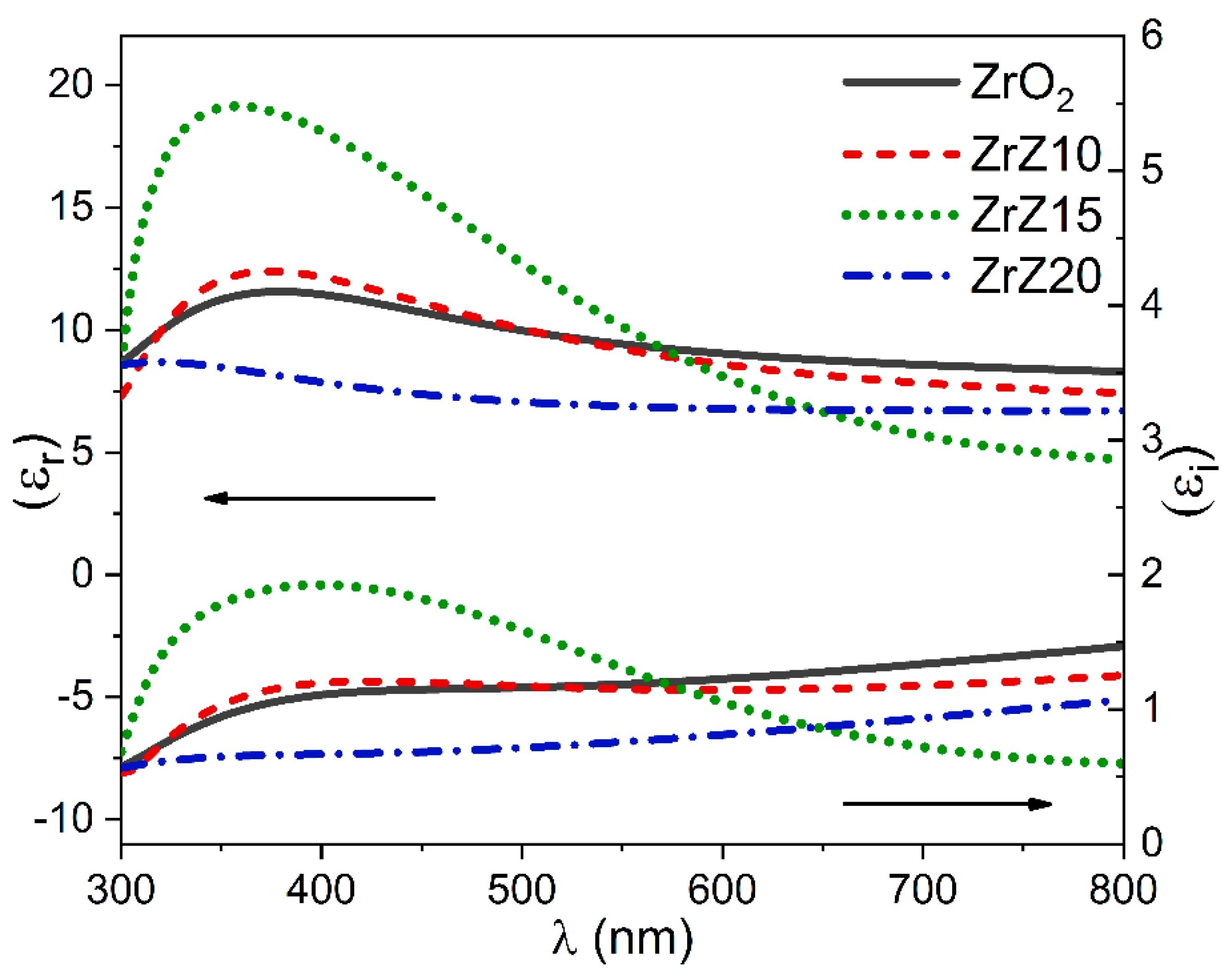
3.2.2. Spectroscopic Ellipsometry (SE) Analysis: Optical Constants

SE is a powerful technique that, without a need of a specific environment, can provide valuable information regarding the optical response of materials and can simultaneously measure the thickness and the optical constants of a multilayer system [45].
In SE, the quantities known as Ψ (amplitude) and Δ (phase angle) corresponding, respectively, to the perpendicular (p) and the parallel (s) components of the light after reflection are measured as a function of wavelength. SE characterization is then carried out with the right choice of the model (based on the reasonable film structure) along with an appropriate optical dispersion oscillator used to fit the spectra. In this study, we opted a three-layer model given as air–ZrO2–glass to simulate the results using widely known Tauc–Lorentz and Cauchy dispersion oscillators with the goal to minimize a mean square error (MSE) function for the best fit between models generated and experimental data. The above-mentioned procedure had been adopted for each sample, and the best fitted data were used to extract thickness (t) (listed in Table 1), optical constants such as refractive index (n) and extinction coefficient (k), and dielectric constant (ε). Moreover, the MSE obtained was ≤1.5, indicating the goodness of the fit obtained for each film sample.
We have chosen pristine ZrO2 film to demonstrate the comparison of model chosen and the experimental data, as indicated by the graph (Ψ (amplitude) and Δ (phase angle) versus wavelength) shown in Figure 6. The fit is excellent for both quantities, as also indicated by MSE = 1.12, confirming the validity of the model. Figure 6 shows that Ψ and Δ have their data features (peak and valley) near shorter wavelength regions, indicating that the film deposited is a thin film [46]. More of these graphs representing the doped samples can be found in the Supplementary Material (Figures S1–S3).
Figure 7 represents the wavelength dispersion of the complex refractive index (n, k), as derived from SE data for ZrO2 and Zn-ZrO2 films, for comparison. One can observe that in general for any selected doping level of Zn, the (n) reveals the same tendency, within two distinct regions of wavelengths from 400 to 800 nm and from 300 to 400 nm. The (n) displays a near plateau in the former region and a slight increase in the latter region. The effect of increasing Zn content on the n values of ZrO2 films, as seen from Figure 7, is quite clear, and we observe that n exhibits a fall as indicated by the values 2.98, 2.89, 2.68, and 2.60 found at 632 nm for ZrO2, ZrZ10, ZrZ15, and ZrZ20 samples, respectively (see Table 2). These values are in agreement with sol-gel-derived ZrO2 films [47]. It is now known that the optical constants of thin films are strongly governed by the film microstructure, which is also subjected to variations induced by deposition/doping parameters. Film microstructure is a combination of morphology and the structure. The former is governed mainly by the porosity and the roughness of the films, and the latter links more with the composition of the materials chosen. Following the structural investigations in these films (discussed above) and these considerations, we can suggest that the structural disorder presumably preponderate over the morphological considerations. Moreover, since addition of Zn creates more defects in ZrO2 films, the observed decrease in n can also be linked with decreasing packing density. This is also in accordance with an earlier finding [48] that the refractive index of zirconia decreases when the lattice defects increase.
The absolute values of n (2.8–3.5), observed for pristine ZrO2 film in this study, are greater than those (2–2.75) reported previously for amorphous ZrO2 films fabricated via sputtering [40,49]. The amorphous film tends to exhibit relatively low values of n when compared with their crystalline counterparts, mainly due to lower packing density in the amorphous state. The amorphous ZrO2 films produced in this work display a relatively higher n, which shows that the film already has a high packing density as well as a low concentration of scattering centers. This again proves that the technique presented in this work is high performance. However, previous reports (which are not many) on Zn-ZrO2 have studied the films for applications specific characteristics, which somehow do not allow for comparisons with their results. Moreover, the n (>2.15) obtained for such low-cost and ecofriendly ZrO2 film make it highly attractive for applications such as high index contrast broadband mirrors and stack coating designs for narrow-band filters [50,51].
A wavelength dispersion of k exhibit a similar trend to n, as indicated in Figure 7 (left side). The k values in the spectral region (300–800 nm) are of the order of 10−1, which indicates good surface homogeneity of the films produced. These values measured at 632 nm are 0.21, 0.19, 0.17, and 0.16 for ZrO2, ZrZ10, ZrZ15, and ZrZ20 samples, respectively (see Table 2) and are higher than the 0.14 value observed for yttrium-doped ZrO2 film [52], and sputtered ZrO2 film [53]. The higher values of k observed for Zn-ZrO2 films in this study are attributed to the high packing density and scattering losses. Scattering may be a result of increased grain size upon increasing Zn content. However, we are not sure which of these reasons dominates over the other. These findings demonstrate that the optical properties of ZrO2 thin films are influenced by the doping level of the Zn, and also, these properties are no less in performance than those obtained through sophisticated deposition technique making water-based solution processing a reliable technique for future technologies.
The dielectric constant of a material is analyzed in two parts, real εr and imaginary εi. Figure 8 represents both parts as derived from ellipsometry data, for all the films. Real part εr for the pristine ZrO2 film remains in the range of 10–11 over the entire spectral range. For example, the value of εr at 400 nm is 8.69 and is greater than the previously reported value observed for amorphous ZrO2 films deposited by atomic layer deposition [54,55]. The absence of any specific feature in the εi spectra is an indication that the films apparently have no crystalline phase present whatsoever.
The results acquired so far in this study are sufficient for us to make the following statement: (i) for dielectric design, in addition to the high dielectric constant the film should be smooth and homogeneous. ZrO2 films produced by using a relatively simple and ecofriendly water-based solution processing are not only fairly smooth over a large area but also exhibit a justly reasonable value of the dielectric constant, so one can make the most of this study by enhancing it further towards optimization for optimal performance. (ii) Moreover, our results imply that doped films are predominantly amorphous but have a smaller band gap than the pristine film; this leads us to consider the potential of these films as smooth channel layers that could produce smooth interfaces to the gate insulator in device applications and should, therefore, be considered a subject of electrical investigations in future studies.

3.2.3. Photoluminescence (PL) Studies

The emissions observed in PL spectra are generally categorized as UV emission and visible emission associated with near band edge emission and defects mediated emissions, respectively. The luminescence mechanism in ZrO2 [56] characterize emissions that mainly come from F&F+-center defects, which not only depend upon the deposition procedure but on the dopant as well. In this context, it is now known that solution processing [57] can possibly introduce a large number of defects known as vacancies and interstitials in oxides films, which introduce the gap states in the host lattice. These defect states together with those introduced by the dopant, such as Zn in ZrO2 in this case, can modify the emissions in PL spectra and characterize the defects/disorder present in the film.
The PL spectra of all the samples in Figure 9 show a sharp peak in the UV region at 344 nm and broad visible emissions around 450 nm. These emissions were de-convoluted using Lorentz distribution function, and we observe that they exhibit nearly similar shape with little variations in positions, intensity, and in full width at half maximum (FWHM), when comparison is being made between pristine and Zn-doped ZrO2 films. This information is listed in Table 3. De-convolution of spectra, as shown in Figure 9, produce three peaks such as peak (1) at 344 nm (3.60 eV) in the UV region, peak (2) at 431 nm (2.87 eV), and peak (3) at 478 nm (2.59 eV) in the visible region. The UV peak, which represents the near band edge emissions sometimes loses its intensity to the trap states near the band edges formed by the defects and vacancies in the oxides films. However, the existence of a sharp UV emission obtained in this study, thus, manifests a fewer trapping centers in the films and being prominently intense than the visible emissions represents the good structural quality [58] in terms of fewer defects/ traps in the synthesized films whether pristine or doped. Therefore, the specific solution processing adopted to fabricate Zn-ZrO2 thin films holds the potential to produce strong UV emitting ZrO2 films. The UV/Vis PL peak intensity, calculated for all the samples, is given in Table 3. It can be noted that the sample ZrZ10 has the highest UV/Vis ratio in all the samples. However, this ratio decreases only for the sample with maximum level of Zn doping, which allows us to draw the conclusion that the doping of Zn in ZrO2 has not only destroyed the surface states/defects that are characterized as emission centers but has also caused activation of the non-radiative defects that become detrimental for PL emission.
The visible peaks designated as peak (2) at 431 nm (2.87 eV) and peak (3) at 478 nm (2.59 eV), as seen in Figure 9, lie in the blue region of visible spectrum and, therefore, are assigned to the electronic transitions from singly ionized oxygen vacancy (F-F+) defect states to the ground state [59]. We can speculate that as a result of excitation, the electron is trapped by the F+ center changing it into an F center and a hole. Subsequently the recombination of F center (with hole) via mid gap levels leads to emission of light. Nonetheless, as a result of Zn doping in ZrO2 films, we have observed that the peak (2) became broader as well as blue shifted and went less pronounced as compared to that for pristine ZrO2 film (see Table 3). The blue shift may be attributed to new defect states introduced by doping, and the peak broadening may be ascribed to the absorptions that take place with charge transfer within the F centers when the doping level of Zn in ZrO2 is increased. Peak (2) observed in this work is comparable to the 434 nm (2.85 eV) PL emission band observed for ZrO2 thin film prepared by the sol gel dip coating technique [26] and the peak shift, as a result of doping, towards 428 nm can be regarded comparable to the peak observed at 425 nm in manganese-doped ZrO2 thin films [60]; the latter has been linked with transitions emanating from defect states related to oxygen vacancies and Zr interstitials. Peak (3) at 478 (2.59 eV) nm observed for ZrO2 film is blue shifted to 474 nm with an increasing doping level of Zn doping (see Table 3). This is comparable to the 471 nm peak observed for Ti-doped ZrO2 thin films prepared via solid state method [57]. The results produced here are, therefore, in agreement with the reported literature and also comparable with the energy range (2.08 and 4.19 eV above the valence band) reported for optical transitions that involve F centers in ZrO2 thin films [61].
Figure 9 further indicates that PL intensity of ZrO2 thin film is reduced when doped with Zn, although when the doping is maximum (sample ZrZ20), it increases but stays below that of the pristine ZrO2. The quenching of the PL intensity in Zn-doped ZrO2 is a clear manifestation of enhanced density of non-radiative recombination centers. The introduction of Zn into the ZrO2 host matrix lifts the defect density/structural imperfection as supported by our structural analysis of these films as well. However, our solution processing method has produced films with minimal defects as indicated by the presence of a sharp UV emission.

4. Conclusions

Until now, Zn-ZrO2 nanoparticles and films have been investigated mostly from the view point of catalytic applications and have in fact outdone their pristine parts with their promising performance; but a complete grip on their properties induced by amount of dopant is missing. This report presents successful implementation of an ecofriendly water-based solution processing to produce Zn-ZrO2 thin films on simple glass substrates, avoiding the sol gel route completely. The correlation developed between doped and pristine film samples has given a good comprehension of how structural and optical behavior of ZrO2 films alter when incorporated with Zn.
We observe that all the variations in the dopant concentration (0, 10, 15, and 20 at.%) bring no change to the structural phase of ZrO2 films; which retains the amorphous phase (found from XRD and Raman studies), whereas Zn plays an important role in changing the surface morphology and optical properties. From the Raman studies, despite the amorphous phase observed in all the doped films, ZnO is recorded by its signature phonon mode present. Studying the surface morphologies using AFM and SEM, it is seen that all the film samples are apparently compact and crack free, exhibiting mean roughness below 2 nm reflecting smooth surfaces; the addition of Zn results in controlling the grains’ configuration in the produced films. All the films are highly transparent (T ≥ 80%) and the Zn doping induces a red shift of the absorption edge of about 1.21 eV in 5.21 eV band gap of pristine ZrO2. The addition of Zn contributes to enhanced defects in these films, which in turn, leads to change in the optical constants such as refractive index and PL intensity. The former is indicated by the Raman spectra, by the band edge states tailing the absorption near the band edges, and by the reduced PL intensity. A high value of refractive index > 2 observed for all the films indicates high packing density of these films obtained from a low-cost solution processed method. Conferring to the PL spectra, we speculate that the blue emissions emerging from oxygen vacancy F+ centers and the emission-intensity dependence on the doping level are characterized by the changes in the concentrations of oxygen vacancies and non-radiative defects brought about by Zn into ZrO2 films. More interestingly, UV emissions remain more intense than visible emissions, indicating the good quality of the films. The study, therefore, shows that this simple ecofriendly deposition route has the potential to produce Zn-ZrO2 films with qualities on a par with those produced from sophisticated techniques, thereby making them suitable for a variety of applications for low-cost ecofriendly technologies and that the control of the precursor ratios in Zn-doped ZrO2 thin films can influence the properties such as grain size and the oxygen vacancies significantly. Therefore, the Zn-ZrO2-based films studied in the present work need to be investigated in more detail with respect to their dielectric and electrical properties for high-quality device applications.

Supplementary Materials

The following are available online at https://www.mdpi.com/article/10.3390/coatings11080901/s1, Figure S1: The graph of (Ψ, Δ) and wavelength, representing the doped sample ZrZ10, obtained from SE, Figure S2: The graph of (Ψ, Δ) and wavelength, representing the doped sample ZrZ15, obtained from SE, Figure S3: The graph of (Ψ, Δ) and wavelength, representing the doped sample ZrZ20, obtained from SE.

Author Contributions

Conceptualization, A.B.; investigation, A.B.; methodology and data acquisition, H.S.; formal analysis A.B.; writing—review and editing, A.B.; resources, S.N. and A.S.B. All authors have read and agreed to the published version of the manuscript.

Funding

This research received no external funding.

Institutional Review Board Statement

Not applicable.

Informed Consent Statement

Not applicable.

Data Availability Statement

Not applicable.

Acknowledgments

A.B. is grateful to National University of Science and Technology, Islamabad, for allowing use of XRD and SEM for this report.

Conflicts of Interest

The authors declare no conflict of interest.

References

  1. Bashir, A.; Wöbkenberg, P.H.; Smith, J.; Ball, J.M.; Adamopoulos, G.; Bradley, D.D.C.; Anthopoulos, T.D. High-performance zinc oxide transistors and circuits fabricated by spray pyrolysis in ambient atmosphere. Adv. Mater. 2009, 21, 2226–2231. [Google Scholar] [CrossRef]
  2. Chen, D.; Xu, J.; Shen, G. Fully transparent flexible transistors built on metal oxide nanowires. Front. Optoelectron. China 2010, 3, 217–227. [Google Scholar] [CrossRef]
  3. Görrn, P.; Sander, M.; Meyer, J.; Kröger, M.; Becker, E.; Johannes, H.-H.; Kowalsky, W.; Riedl, T. Towards see-through displays: Fully transparent thin-film transistors driving transparent organic light-emitting diodes. Adv. Mater. 2006, 18, 738–741. [Google Scholar] [CrossRef]
  4. Glynn, C.; O’Dwyer, C. Solution processable metal oxide thin film deposition and material growth for electronic and photonic devices. Adv. Mater. Interfaces 2017, 4, 1600610. [Google Scholar] [CrossRef]
  5. Balog, M.; Schieber, M.; Michman, M.; Patai, S. The chemical vapour deposition and characterization of ZrO2 films from organometallic compounds. Thin Solid Film. 1977, 47, 109–120. [Google Scholar] [CrossRef]
  6. Ibrahim, M.M. Photocatalytic activity of nanostructured ZnO–ZrO2 binary oxide using fluorometric method. Spectrochim. Acta A Mol. Biomol. Spectrosc. 2015, 145, 487–492. [Google Scholar] [CrossRef]
  7. Liu, G.X.; Liu, A.; Shan, F.K.; Meng, Y.; Shin, B.C.; Fortunato, E.; Martins, R. High-performance fully amorphous bilayer metal-oxide thin film transistors using ultra-thin solution-processed ZrOx dielectric. Appl. Phys. Lett. 2014, 105, 113509. [Google Scholar] [CrossRef]
  8. Oluwabi, A.T.; Katerski, A.; Carlos, E.; Branquinho, R.; Mere, A.; Krunks, M.; Fortunato, E.; Pereira, L.; Oja Acik, I. Application of ultrasonic sprayed zirconium oxide dielectric in zinc tin oxide-based thin film transistor. J. Mater. Chem. C 2020, 8, 3730–3739. [Google Scholar] [CrossRef]
  9. Zegtouf, H.; Saoula, N.; Azibi, M.; Bait, L.; Madaoui, N.; Khelladi, M.R.; Kechouane, M. A study of properties of ZrO2 thin films deposited by magnetron sputtering under different plasma parameters: Biomedical application. J. Electr. Eng. 2019, 70, 117. [Google Scholar] [CrossRef] [Green Version]
  10. Häfele, E.; Kaltenmaier, K.; Schönauer, U. Application of the ZrO2 sensor in determination of pollutant gases. Sens. Actuators B Chem. 1991, 4, 525–527. [Google Scholar] [CrossRef]
  11. Khan, M.A.; Gondal, M.A.; Khawaja, E.E. A gas pressure sensor based on ZrO2 thin films for use at high temperatures. Int. J. Electron. 2000, 87, 227–234. [Google Scholar] [CrossRef]
  12. Velumani, M.; Meher, S.R.; Balakrishnan, L.; Sivacoumar, R.; Alex, Z.C. ZrO2-ZnO composite thin films for humidity sensing. In Proceedings of the AIP Conference, Uttar Pradesh, India, 21–25 December 2016; p. 080032. [Google Scholar]
  13. Stefanov, P.; Atanasova, G.; Marinova, T.; Gómez-García, J.; Sanz, J.M.; Caballero, A.; Morales, J.J.; Cordón, A.M.; González-Elipe, A.R. Characterization of Co/ZrO2 de-NOx thin film catalysts prepared by magnetron sputtering. Cata. Lett. 2003, 90, 195–203. [Google Scholar] [CrossRef]
  14. You, Q.; Cai, H.; Hu, Z.; Liang, P.; Prucnal, S.; Zhou, S.; Sun, J.; Xu, N.; Wu, J. Blue shift in absorption edge and widening of band gap of ZnO by Al doping and Al–N co-doping. J. Alloys Compd. 2015, 644, 528–533. [Google Scholar] [CrossRef]
  15. Kołodziejczak-Radzimska, A.; Jesionowski, T. Zinc Oxide-from synthesis to application: A Review. Materials 2014, 7, 2833–2881. [Google Scholar] [CrossRef] [PubMed] [Green Version]
  16. Hayashi, H.; Yoshida, O.; Suzuki, H. ZnO-ZrO2 films with good UV-shielding properties prepared by a single step sol-gel method. J. Ceram. Soc. Jpn. 2009, 117, 978–982. [Google Scholar] [CrossRef] [Green Version]
  17. Uribe López, M.C.; Alvarez Lemus, M.A.; Hidalgo, M.C.; López González, R.; Quintana Owen, P.; Oros-Ruiz, S.; Uribe López, S.A.; Acosta, J. Synthesis and characterization of ZnO-ZrO2 nanocomposites for photocatalytic degradation and mineralization of phenol. J. Nanomater. 2019, 2019, 1015876. [Google Scholar] [CrossRef] [Green Version]
  18. Aghabeygi, S.; Khademi-Shamami, M. ZnO/ZrO2 nanocomposite: Sonosynthesis, characterization and its application for wastewater treatment. Ultrason. Sonochem. 2018, 41, 458–465. [Google Scholar] [CrossRef]
  19. Precious Ayanwale, A.; Reyes-López, S.Y. ZrO2–ZnO nanoparticles as antibacterial agents. ACS Omega. 2019, 4, 19216–19224. [Google Scholar] [CrossRef] [Green Version]
  20. Bashir, M.; Ashraf, A.; Imtiaz, M.; Riaz, S.; Naseem, S. Synthesis and Characterization of ZrO2-ZnO Nanoparticles. In Proceedings of the World Congress on Advances in Nano Biomechanics, Robotics and Energy Research (ANBRE), Seoul, Korea, 25–28 August 2013. [Google Scholar]
  21. Li, Y.; Liu, M. Gas sensing properties of Y-doped ZnO nanosheets synthesized via combustion method. Trans. Nonferrous. Met. Soc. 2015, 25, 2247–2252. [Google Scholar] [CrossRef]
  22. Meyers, S.T.; Anderson, J.T.; Hung, C.M.; Thompson, J.; Wager, J.F.; Keszler, D.A. Aqueous inorganic inks for low-temperature fabrication of ZnO TFTs. J. Am. Chem. Soc. 2008, 130, 17603–17609. [Google Scholar] [CrossRef] [PubMed]
  23. Bashir, A.; Farooq, M.; Malik, A.; Naseem, S.; Bhatti, A.S. UV-a treatment of ZrO2 thin films fabricated by environmental friendlier water-based solution processing: Structural and optical studies. Coatings 2021, 11, 821. [Google Scholar] [CrossRef]
  24. Bashir, A.; Majeed, A.; Naseem, S.; Bhatti, A.S. Investigation of structural and optical parameters of yttrium-doped ZnO thin films prepared via spin coating of simple aqueous solution. Bull. Mater. Sci. 2021, 44, 95. [Google Scholar] [CrossRef]
  25. Keramidas, V.G.; White, W.B. Raman scattering study of the crystallization and phase transformations of ZrO2. J. Am. Ceram. Soc. 1974, 57, 22–24. [Google Scholar] [CrossRef]
  26. Méndez-López, A.; Zelaya-Ángel, O.; Toledano-Ayala, M.; Torres-Pacheco, I.; Pérez-Robles, J.F.; Acosta-Silva, Y.J. The influence of annealing temperature on the structural and optical properties of ZrO2 thin films and how affects the hydrophilicity. Crystals 2020, 10, 454. [Google Scholar] [CrossRef]
  27. Li, Z.; Su, K. The direct reaction between CO2 and phenol catalyzed by bifunctional catalyst ZrO2. J. Mol. Catal. A Chem. 2007, 277, 180–184. [Google Scholar] [CrossRef]
  28. Lin, C.; Zhang, C.; Lin, J. Phase transformation and photoluminescence properties of nanocrystalline ZrO2 powders prepared via the pechini-type sol−gel process. J. Phys. Chem. C 2007, 111, 3300–3307. [Google Scholar] [CrossRef]
  29. Ariza, R.; Dael, M.; Sotillo, B.; Urbieta, A.; Solis, J.; Fernández, P. Vapor-solid growth ZnO:ZrO2 micro and nanocomposites. J. Alloys Compd. 2021, 877, 160219. [Google Scholar] [CrossRef]
  30. Ivanova, T.; Harizanova, A.; Koutzarova, T.; Vertruyen, B. Effect of annealing temperatures on properties of sol-gel grown ZnO-ZrO2 films. Cryst. Res. Technol. 2010, 45, 1154–1160. [Google Scholar] [CrossRef]
  31. Ji, P.; Mao, Z.; Wang, Z.; Xue, X.; Zhang, Y.; Lv, J.; Shi, X. Improved surface-enhanced raman scattering properties of ZrO2 nanoparticles by Zn doping. Nanomaterials 2019, 9, 983. [Google Scholar] [CrossRef] [PubMed] [Green Version]
  32. Gorin, A.; Copperwhite, R.; Elmaghrum, S.; Mc Donagh, C.; Oubaha, M. Hybrid zirconium sol-gel thin films with high refractive index. In Proceedings of the SPIE International Symposium on Photoelectronic Detection and Imaging: Sensor and Micromachined Optical Device Technologies, Beijing, China, 8 September 2011. [Google Scholar]
  33. Benyagoub, A.; Levesque, F.; Couvreur, F.; Gibert-Mougel, C.; Dufour, C.; Paumier, E. Evidence of a phase transition induced in zirconia by high energy heavy ions. Appl. Phys. Lett. 2000, 77, 3197–3199. [Google Scholar] [CrossRef]
  34. Strekalovskii, V.N.; Vovkotrub, É.G. Raman spectroscopy of materials based on zirconium dioxide. Refractories 1985, 26, 151–162. [Google Scholar] [CrossRef]
  35. Davydova, A.; Tselikov, G.; Dilone, D.; Rao, K.; Kabashin, A.; Belova, L. Fabrication of thin ZnO films with wide-range tuned optical properties by reactive magnetron sputtering. Semicond. Sci. Tech. 2017, 33, 025004. [Google Scholar] [CrossRef]
  36. Kunj, S.; Sreenivas, K. Residual stress and defect content in magnetron sputtered ZnO films grown on unheated glass substrates. Curr. Appl. Phys. 2016, 16, 748–756. [Google Scholar] [CrossRef]
  37. Patel, U.S.; Patel, K.H.; Chauhan, K.V.; Chawla, A.K.; Rawal, S.K. Investigation of various properties for zirconium oxide films synthesized by sputtering. Procedia Technol. 2016, 23, 336–343. [Google Scholar] [CrossRef] [Green Version]
  38. Takahashi, T.; Nakabayashi, H.; Terasawa, T.; Masugata, K. Atomic force microscopy observation of TiO2 films deposited by dc reactive sputtering. J. Vac. Sci. Technol. A 2002, 20, 1205–1209. [Google Scholar] [CrossRef]
  39. Nayak, P.K.; Hedhili, M.N.; Cha, D.; Alshareef, H.N. High performance In2O3 thin film transistors using chemically derived aluminum oxide dielectric. Appl. Phys. Lett. 2013, 103, 033518. [Google Scholar] [CrossRef] [Green Version]
  40. Hojabri, A. Structural and optical characterization of ZrO2 thin films grown on silicon and quartz substrates. J. Theor. Appl. Phys. 2016, 10, 219–224. [Google Scholar] [CrossRef] [Green Version]
  41. French, R.H.; Glass, S.J.; Ohuchi, F.S.; Xu, Y.N.; Ching, W.Y. Experimental and theoretical determination of the electronic structure and optical properties of three phases of ZrO2. Phys. Rev. B 1994, 49, 5133–5142. [Google Scholar] [CrossRef] [PubMed]
  42. Navio, J.A.; Hidalgo, M.C.; Colon, G.; Botta, S.G.; Litter, M.I. Preparation and physicochemical properties of ZrO2 and Fe/ZrO2 prepared by a sol−gel technique. Langmuir 2001, 17, 202–210. [Google Scholar] [CrossRef]
  43. Pan, Y.; Inam, F.; Zhang, M.; Drabold, D.A. Atomistic origin of urbach tails in amorphous silicon. Phys. Rev. Lett. 2008, 100, 206403. [Google Scholar] [CrossRef] [Green Version]
  44. Harrop, P.J.; Wanklyn, J.N. The dielectric constant of zirconia. Br. J. Appl. Phys. 1967, 18, 739–742. [Google Scholar] [CrossRef]
  45. Yusoh, R.; Horprathum, M.; Eiamchai, P.; Chindaudom, P.; Aiempanakit, K. Determination of optical and physical properties of ZrO2 films by spectroscopic ellipsometry. Procedia Eng. 2012, 32, 745–751. [Google Scholar] [CrossRef] [Green Version]
  46. Fujiwara, H. Spectroscopic Ellipsometry: Principles and Applications; John Wiley & Sons, Ltd.: Hoboken, NJ, USA, 2007. [Google Scholar]
  47. Yoon, J.J.; Lee, S.M.; Kim, T.J.; Hwang, S.Y.; Diware, M.; Kim, Y.D.; Hwang, S.M.; Joo, J. Optical study of sol-gel processed ZrO2/Si films by spectroscopic ellipsometry. J. Vac. Sci. Technol. B 2011, 29, 04D108. [Google Scholar] [CrossRef]
  48. Zhao, S.; Ma, F.; Xu, K.W.; Liang, H.F. Optical properties and structural characterization of bias sputtered ZrO2 films. J. Alloys Compd. 2008, 453, 453–457. [Google Scholar] [CrossRef]
  49. Sunke, V.; Bukke, G.N.; Suda, U. Characterisation of nanostructured ZrO2 thin films formed by DC reactive magnetron sputtering. J. Nanomed. Res. 2018, 7, 65–68. [Google Scholar]
  50. Southwell, W.H.; Hall, R.L. Rugate filter sidelobe suppression using quintic and rugated quintic matching layers. Appl. Opt. 1989, 28, 2949–2951. [Google Scholar] [CrossRef] [PubMed]
  51. Lorenzo, E.; Oton, C.J.; Capuj, N.E.; Ghulinyan, M.; Navarro-Urrios, D.; Gaburro, Z.; Pavesi, L. Porous silicon-based rugate filters. Appl. Opt. 2005, 44, 5415–5421. [Google Scholar] [CrossRef] [PubMed] [Green Version]
  52. Sal’nikov, V.V. Influence of F centers on the optical and adsorptive properties of doped ZrO2 crystals. Inorg. Mater. 2000, 36, 479–483. [Google Scholar] [CrossRef]
  53. Juškevičius, K.; Audronis, M.; Subačius, A.; Drazdys, R.; Juškėnas, R.; Matthews, A.; Leyland, A. High-rate reactive magnetron sputtering of zirconia films for laser optics applications. Appl. Phys. A 2014, 116, 1229–1240. [Google Scholar] [CrossRef]
  54. Sayan, S.; Nguyen, N.V.; Ehrstein, J.; Emge, T.; Garfunkel, E.; Croft, M.; Zhao, X.; Vanderbilt, D.; Levin, I.; Gusev, E.P.; et al. Structural, electronic, and dielectric properties of ultrathin zirconia films on silicon. Appl. Phys. Lett. 2005, 86, 152902. [Google Scholar] [CrossRef] [Green Version]
  55. An, I.; Lee, S.; Kang, B.; Lee, S.; Jeong, H.; Song, C. Optical, electrical, and structural properties of ultrathin zirconium-oxide films. J. Korean Phys. Soc. 2010, 57, 1811–1815. [Google Scholar] [CrossRef]
  56. Arsenev, P.A.; Bagdasarov, K.S.; Niklas, A.; Ryazantsev, A.D. X-ray and thermostimulated luminescence of 0.9 ZrO2–0.1 Y2O3 single crystals. Phys. Status. Solidi (a) 1980, 62, 395–398. [Google Scholar] [CrossRef]
  57. Cong, Y.; Li, B.; Lei, B.; Li, W. Long lasting phosphorescent properties of Ti doped ZrO2. J. Lumin. 2007, 126, 822–826. [Google Scholar] [CrossRef]
  58. Kumari, L.; Li, W.Z.; Xu, J.M.; Leblanc, R.M.; Wang, D.Z.; Li, Y.; Guo, H.; Zhang, J. Controlled hydrothermal synthesis of zirconium oxide nanostructures and their optical properties. Cryst. Growth. Des. 2009, 9, 3874–3880. [Google Scholar] [CrossRef]
  59. Wang, Z.; Yang, B.; Fu, Z.; Dong, W.; Yang, Y.; Liu, W. UV–blue photoluminescence from ZrO2 nanopowders prepared via glycine nitrate process. Appl. Phys. A 2005, 81, 691–694. [Google Scholar] [CrossRef]
  60. Pattanaik, S.; Martha, S.; Sharma, M.K.; Pradhan, S.K.; Sakthivel, R.; Chatterjee, R.; Mishra, D.K. Enhancement of room temperature ferromagnetism in nanocrystalline Zr1−xMnxO2 by the suppression of monoclinic structure of zirconia. J. Magn. Magn. Mater. 2020, 494, 165768. [Google Scholar] [CrossRef]
  61. Imparato, C.; Fantauzzi, M.; Passiu, C.; Rea, I.; Ricca, C.; Aschauer, U.; Sannino, F.; D’Errico, G.; De Stefano, L.; Rossi, A.; et al. Unraveling the charge state of oxygen vacancies in ZrO2–x on the basis of synergistic computational and experimental evidence. J. Phys. Chem. C 2019, 123, 11581–11590. [Google Scholar] [CrossRef]
Figure 1. The XRD patterns of pristine and Zn-ZrO2 films are shown here. A clear broad band appearing around 25° depicts amorphous phase observed in all the films irrespective of the doping level.
Coatings 11 00901 g001
Figure 2. Raman spectra of ZrO2 thin films at different doping level of Zn are shown here. Absence of distinct phonon band indicates the presence of amorphous phase but the phonon band occurring around 562 cm−1 indicates the presence of Zn in the doped samples only.
Coatings 11 00901 g002
Figure 3. 3D-AFM images for pristine ZrO2 film (a) and for Zn-doped samples (bd). The films indicate the appearance and reconfiguration of grains as the dopant concentration is varied.
Coatings 11 00901 g003
Figure 4. SEM images of (a) ZrO2 thin films at different doping level of Zn: (b) 10 at.%, (c) 15 at.%, and (d) 20 at.%. The white scale bars at the bottom covers 1 µm thereby indicating a large area of the film viewed.
Coatings 11 00901 g004
Figure 5. (a) Optical transmittance (T) spectra, obtained for all the samples, is plotted against the incident wavelength. Films are highly transparent in the visible region and a change in optical band gap is also evident from the fall observed in T, in the UV region. (b) The set of Tauc plots, for all the samples, used to evaluate the band gap energy Eg of each film.
Coatings 11 00901 g005
Figure 6. Experimental and fitted SE data for both phase (Δ) and amplitude (Ψ) for pristine ZrO2 sample. Similar fitting with mean square error below 1.5 was obtained for doped samples as well, which have been provided in the Supplementary information.
Coatings 11 00901 g006
Figure 7. Refractive index (n) on left and extinction coefficient (k) on right are plotted against wavelength for all the samples.
Coatings 11 00901 g007
Figure 8. Both parts of dielectric constants (real εr on left and imaginary εi on right) are plotted against wavelength for all the samples.
Coatings 11 00901 g008
Figure 9. PL spectra (plotted against wavelength) for various levels of Zn dopant in ZrO2 films. Pronounced UV emission as compared to blue emission indicates a good structural quality of all the films. The spectra for samples ZrZ10 and ZrZ15 are overlapped.
Coatings 11 00901 g009
Table 1. Sample identification scheme, grain size, surface roughness, and other parameters (obtained from Raman spectroscopy) for pristine and Zn-doped ZrO2 thin films.
Sample IDZn Content
(at.%)
Grain Size
(nm)
RoughnessZnO-A1 LO
Raman Mode (cm−1)
Fwhm-A1 LO Mode (cm−1)
Rq(nm)Ra(nm)
ZrO20-1.591.15--
ZrZ101023.251.971.26562.78 114.98 ± 19.40
ZrZ151515.501.881.32561.9016.02 ± 4.82
ZrZ202038.092.181.53576.93312.80 ± 71.25
Table 2. Optical parameters obtained for pristine and Zn-doped ZrO2 thin films.
Sample IDThickness
(nm)
Transmittance
T (%)
Eg
(eV)
Eu
(eV)
n
at 632 nm
k
at 632 nm
ZrO268.64835.210.692.980.21
ZrZ1070.00864.271.912.880.19
ZrZ1571.50814.003.042.670.17
ZrZ2071.52854.663.362.600.16
Table 3. Peaks positions, FWHM, and ratio of UV to visible emission obtained from PL analysis of all samples.
Sample IDPeak 1 (nm)
FWHM (nm)
Peak 2 (nm)
FWHM (nm)
Peak 3 (nm)
FWHM (nm)
UV/Vis Ratio
ZrO23444314784.92 ± 0.48
12.5 ± 0.152.5 ± 2.592.8 ± 5.5-
ZrZ103434284745.33 ± 0.5
13.1 ± 0.153.8 ± 2.587.7 ± 4.9-
ZrZ153434304745.00± 0.47
13.1 ± 0.152.9 ± 2.484.9 ± 1.9-
ZrZ203434304744.25 ± 0.5
12.9 ± 0.154.32 ± 2.180.37 ± 4.2-
Publisher’s Note: MDPI stays neutral with regard to jurisdictional claims in published maps and institutional affiliations.

