
Structural, Optical, and Electrical Properties of Copper Oxide Films Grown by the SILAR Method with Post-Annealing


Abstract
:1. Introduction
2. Materials and Methods
2.1. Samples Preparation
2.2. Samples Characterization
3. Results and Discussion
4. Conclusions
Supplementary Materials
Author Contributions
Funding
Institutional Review Board Statement
Informed Consent Statement
Data Availability Statement
Acknowledgments
Conflicts of Interest
References
- Ogwu, A.A.; Darma, T.H.; Bouquerel, E. Electrical resistivity of copper oxide thin films prepared by reactive magnetron sputtering. J. Achiev. Mater. Manuf. Eng. 2007, 24, 172–177. [Google Scholar]
- Yu, J.; Hai, Y.; Jaroniec, M. Photocatalytic hydrogen production over CuO-modified titania. J. Colloid Interface Sci. 2011, 357, 223–228. [Google Scholar] [CrossRef]
- Dasineh Khiavi, N.; Katal, R.; Kholghi Eshkalak, S.; Masudy-Panah, S.; Ramakrishna, S.; Jiangyong, H. Visible light driven heterojunction photocatalyst of CuO-Cu2O thin films for photocatalytic degradation of organic pollutants. Nanomaterials 2019, 9, 1011. [Google Scholar] [CrossRef] [PubMed] [Green Version]
- Rydosz, A. The use of copper oxide thin films in gas-sensing applications. Coatings 2018, 8, 425. [Google Scholar] [CrossRef] [Green Version]
- Steinhauer, S. Gas sensors based on copper oxide nanomaterials: A review. Chemosensors 2021, 9, 51. [Google Scholar] [CrossRef]
- Wang, S.B.; Hsiao, C.H.; Chang, S.J.; Lam, K.T.; Wen, K.H.; Hung, S.C.; Young, S.J.; Huang, B.R. A CuO nanowire infrared photodetector. Sens. Actuators A 2011, 171, 207–211. [Google Scholar] [CrossRef]
- Selman, A.M.; Mahdi, M.A.; Hassan, Z. Fabrication of Cu2O nanocrystalline thin films photosensor prepared by RF sputtering technique. Physica E 2017, 94, 132–138. [Google Scholar] [CrossRef]
- Oku, T.; Yamada, T.; Fujimoto, K.; Akiyama, T. Microstructures and photovoltaic properties of Zn(Al)O/Cu2O-based solar cells prepared by spin-coating and electrodeposition. Coatings 2014, 4, 203–213. [Google Scholar] [CrossRef] [Green Version]
- Alajlani, Y.; Placido, F.; Chu, H.O.; Bold, R.D.; Fleming, L.; Gibson, D. Characterisation of Cu2O/CuO thin films produced by plasma-assisted DC sputtering for solar cell application. Thin Solid Film. 2017, 642, 45–50. [Google Scholar] [CrossRef] [Green Version]
- Park, J.C.; Kim, J.; Kwon, H.; Song, H. Gram-scale synthesis of Cu2O nanocubes and subsequent oxidation to CuO hollow nanostructures for lithium-ion battery anode materials. Adv. Mater. 2009, 21, 803–807. [Google Scholar] [CrossRef]
- Hu, L.; Huang, Y.; Zhang, F.; Chen, Q. CuO/Cu2O composite hollow polyhedrons fabricated from metal–organic framework templates for lithium-ion battery anodes with a long cycling life. Nanoscale 2013, 5, 4186–4190. [Google Scholar] [CrossRef] [PubMed]
- Zhou, L.; He, Y.; Jia, C.; Pavlinek, V.; Saha, P.; Cheng, Q. Construction of hierarchical CuO/Cu2O@NiCo2S4 nanowire arrays on copper foam for high performance supercapacitor electrodes. Nanomaterials 2017, 7, 273. [Google Scholar] [CrossRef] [Green Version]
- Nathan, D.M.G.T.; Boby, S.J.M.; Basu, P.; Mahesh, R.; Harish, S.; Joseph, S.; Sagayaraj, P. One-pot hydrothermal preparation of Cu2O-CuO/rGO nanocomposites with enhanced electrochemical performance for supercapacitor applications. Appl. Surf. Sci. 2018, 449, 474–484. [Google Scholar]
- Rydosz, A.; Dyndał, K.; Andrysiewicz, W.; Grochala, D.; Marszałek, K. GLAD magnetron sputtered ultra-thin copper oxide films for gas-sensing application. Coatings 2020, 10, 378. [Google Scholar] [CrossRef] [Green Version]
- Balamurugan, B.; Mehta, B.R. Optical and structural properties of nanocrystalline copper oxide thin films prepared by activated reactive evaporation. Thin Solid Film. 2001, 396, 90–96. [Google Scholar] [CrossRef]
- Al-Kuhaili, M.F. Characterization of copper oxide thin films deposited by the thermal evaporation of cuprous oxide (Cu2O). Vacuum 2008, 82, 623–629. [Google Scholar] [CrossRef]
- Valladares, L.D.L.S.; Salinas, D.H.; Dominguez, A.B.; Najarro, D.A.; Khondaker, S.I.; Mitrelias, T.; Barnes, C.H.W.; Aguiar, J.A.; Majima, Y. Crystallization and electrical resistivity of Cu2O and CuO obtained by thermal oxidation of Cu thin films on SiO2/Si substrates. Thin Solid Film. 2012, 520, 6368–6374. [Google Scholar] [CrossRef]
- Castrejón-Sánchez, V.H.; Solís, A.C.; López, R.; Encarnación-Gomez, C.; Morales, F.M.; Vargas, O.S.; Mastache-Mastache, J.E.; Sánchez, G.V. Thermal oxidation of copper over a broad temperature range-towards the formation of cupric oxide (CuO). Mater. Res. Express 2019, 6, 075909. [Google Scholar] [CrossRef]
- Kayani, Z.N.; Umer, M.; Riaz, S.; Naseem, S. Characterization of copper oxide nanoparticles fabricated by the sol–gel method. J. Electron. Mater. 2015, 44, 3704–3709. [Google Scholar] [CrossRef]
- Lillo-Ramiro, J.; Guerrero-Villalba, J.M.; Mota-González, M.L.; Aguirre-Tostado, F.S.; Gutiérrez-Heredia, G.; Mejía-Silva, I.; Carrillo-Castillo, A. Optical and microstructural characteristics of CuO thin films by sol gel process and introducing in non-enzymatic glucose biosensor applications. Optik 2021, 229, 166238. [Google Scholar] [CrossRef]
- Zhu, Y.; Xu, Z.; Yan, K.; Zhao, H.; Zhang, J. One-step synthesis of CuO–Cu2O heterojunction by flame spray pyrolysis for cathodic photoelectrochemical sensing of L-cysteine. ACS Appl. Mater. Interfaces 2017, 9, 40452–40460. [Google Scholar] [CrossRef] [PubMed]
- Naveena, D.; Logu, T.; Dhanabal, R.; Sethuraman, K.; Bose, A.C. Comparative study of effective photoabsorber CuO thin films prepared via different precursors using chemical spray pyrolysis for solar cell application. J. Mater. Sci. Mater. Electron. 2019, 30, 561–572. [Google Scholar] [CrossRef]
- Izaki, M.; Fukazawa, K.; Sato, K.; Khoo, P.L.; Kobayashi, M.; Takeuchi, A.; Uesugi, K. Defect structure and photovoltaic characteristics of internally stacked CuO/Cu2O photoactive layer prepared by electrodeposition and heating. ACS Appl. Energy Mater. 2019, 2, 4833–4840. [Google Scholar] [CrossRef]
- Rosas-Laverde, N.M.; Pruna, A.I.; Cembrero, J.; Busquets-Mataix, D. Electrodeposition of ZnO/Cu2O heterojunctions on Ni-Mo-P electroless coating. Coatings 2020, 10, 935. [Google Scholar] [CrossRef]
- Rafea, M.A.; Roushdy, N. Determination of the optical band gap for amorphous and nanocrystalline copper oxide thin films prepared by SILAR technique. J. Phys. D Appl. Phys. 2009, 42, 015413. [Google Scholar] [CrossRef]
- Mageshwari, K.; Sathyamoorthy, R. Physical properties of nanocrystalline CuO thin films prepared by the SILAR method. Mater. Sci. Semicond. Process 2013, 16, 337–343. [Google Scholar] [CrossRef]
- Ravichandran, A.T.; Dhanabalan, K.; Vasuhi, A.; Chandramohan, R.; Mantha, S. Morphology, bandgap, and grain size tailoring in Cu2O thin film by SILAR method. IEEE Trans. Nanotechnol. 2015, 14, 108–112. [Google Scholar] [CrossRef]
- Nikam, S.S.; Suryawanshi, M.P.; Bhosale, S.M.; Gaikwad, M.A.; Shinde, P.A.; Moholkar, A.V. Cu2O thin films prepared using modified successive ionic layer adsorption and reaction method and their use in photoelectrochemical solar cells. J. Mater. Sci. Mater. Electron. 2016, 27, 1897–1900. [Google Scholar] [CrossRef]
- Visalakshi, S.; Kannan, R.; Valanarasu, S.; Kathalingam, A.; Rajashabala, S. Effect of adsorption time on structural, optical and electronic properties of SILAR deposited CuO thin films. J. Mater. Sci. Mater. Electron. 2016, 27, 9179–9185. [Google Scholar] [CrossRef]
- Chatterjee, S.; Saha, S.K.; Pal, A.J. Formation of all-oxide solar cells in atmospheric condition based on Cu2O thin-films grown through SILAR technique. Sol. Energy Mater. Sol. Cells 2016, 147, 17–26. [Google Scholar] [CrossRef]
- Nicolau, Y.F. Solution deposition of thin solid compound films by a successive ionic-layer adsorption and reaction process. Appl. Surf. Sci. 1985, 22–23, 1061–1074. [Google Scholar] [CrossRef]
- Koch, V.M.; Barr, M.K.S.; Büttner, P.; Mínguez-Bacho, I.; Döhler, D.; Winzer, B.; Reinhardt, E.; Segets, D.; Bachmann, J. A solution-based ALD route towards (CH3NH3)(PbI3) perovskite via lead sulfide film. J. Mater. Chem. A 2019, 7, 25112–25119. [Google Scholar] [CrossRef] [Green Version]
- Graniel, O.; Puigmartí-Luis, J.; Muñoz-Rojas, D. Liquid atomic layer deposition as emergent technology for the fabrication of thin films. Dalton Trans. 2021, 50, 6373–6381. [Google Scholar] [CrossRef]
- Bayansal, F.; Kahraman, S.; Ҫankaya, G.; Ҫetinkara, H.A.; Güder, H.S.; Ҫakmak, H.M. Growth of homogenous CuO nano-structured thin films by a simple solution method. J. Alloys Compd. 2011, 509, 2094–2098. [Google Scholar] [CrossRef]
- Jayakrishnan, R.; Kurian, A.S.; Nair, V.G.; Joseph, M.R. Effect of vacuum annealing on the photoconductivity of CuO thin films grown using sequential ionic layer adsorption reaction. Mater. Chem. Phys. 2016, 180, 149–155. [Google Scholar] [CrossRef]
- Ristov, M.; Sinadinovski, G.J. Chemical deposition of Cu2O thin films. Thin Solid Film. 1985, 123, 63–67. [Google Scholar] [CrossRef]
- Nair, M.T.S.; Guerrero, L.; Arenas, O.L.; Nair, P.K. Chemically deposited copper oxide thin films: Structural, optical and electrical characteristics. Appl. Surf. Sci. 1999, 150, 143–151. [Google Scholar] [CrossRef]
- Serin, N.; Serin, T.; Horzum, Ş.; Ҫelik, Y. Annealing effects on the properties of copper oxide thin films prepared by chemical deposition. Semicond. Sci. Technol. 2005, 20, 398–401. [Google Scholar] [CrossRef]
- Johan, M.R.; Suan, M.S.M.; Hawari, N.L.; Ching, H.A. Annealing effects on the properties of copper oxide thin films prepared by chemical deposition. Int. J. Electrochem. Sci. 2011, 6, 6094–6104. [Google Scholar]
- Ravichandran, A.T.; Dhanabalan, K.; Valanarasu, S.; Vasuhi, A.; Kathalingam, A. Role of immersion time on the properties of SILAR deposited CuO thin films. J. Mater. Sci. Mater. Electron. 2015, 26, 921–926. [Google Scholar] [CrossRef]
- Cheng, H.E.; Lee, W.J. Properties of TiN films grown by atomic-layer chemical vapor deposition with a modified gaseous-pulse sequence. Mater. Chem. Phys. 2006, 97, 315–320. [Google Scholar] [CrossRef]
- Balkanski, M.; Nusimovici, M.A.; Reydellet, J. First order Raman spectrum of Cu2O. Solid State Commun. 1969, 7, 815–818. [Google Scholar] [CrossRef]
- Yu, P.Y.; Shen, Y.R.; Petroff, Y.; Falicov, L.M. Resonance Raman scattering at the forbidden yellow exciton in Cu2O. Phys. Rev. Lett. 1973, 30, 283–286. [Google Scholar] [CrossRef]
- Dawson, P.; Hargreave, M.M.; Wilkinson, G.R. The dielectric and lattice vibrational spectrum of cuprous oxide. J. Phys. Chem. Solids 1973, 34, 2201–2208. [Google Scholar] [CrossRef]
- Yu, P.Y.; Shen, Y.R. Resonance Raman studies in Cu2O. I. The phonon-assisted 1s yellow excitonic absorption edge. Phys. Rev. B 1975, 12, 1377–1394. [Google Scholar] [CrossRef]
- Mao, Y.; He, J.; Sun, X.; Li, W.; Lu, X.; Gan, J.; Liu, Z.; Gong, L.; Chen, J.; Liu, P.; et al. Electrochemical synthesis of hierarchical Cu2O stars with enhanced photoelectrochemical properties. Electrochim. Acta 2012, 62, 1–7. [Google Scholar] [CrossRef]
- Singhal, A.; Pai, M.R.; Rao, R.; Pillai, K.T.; Lieberwirth, I.; Tyagi, A.K. Copper(I) oxide nanocrystals—One step synthesis, characterization, formation mechanism, and photocatalytic properties. Eur. J. Inorg. Chem. 2013, 2013, 2640–2651. [Google Scholar] [CrossRef]
- Wang, Z.; Pischedda, V.; Saxena, S.K.; Lazor, P. X-ray diffraction and Raman spectroscopic study of nanocrystalline CuO under pressures. Solid State Commun. 2002, 121, 275–279. [Google Scholar] [CrossRef]
- Wang, W.; Zhou, Q.; Fei, X.; He, Y.; Zhang, P.; Zhang, G.; Peng, L.; Xie, W. Synthesis of CuO nano- and micro-structures and their Raman spectroscopic studies. CrystEngComm 2010, 12, 2232–2237. [Google Scholar] [CrossRef]
- Nwanya, A.C.; Obi, D.; Ozoemena, K.I.; Osuji, R.U.; Awada, C.; Ruediger, A.; Maaza, M.; Rosei, F.; Ezema, F.I. Facile synthesis of nanosheet-like CuO film and its potential application as a high-performance pseudocapacitor electrode. Electrochim. Acta 2016, 198, 220–230. [Google Scholar] [CrossRef]
- Lee, W.J.; Hon, M.H.; Chung, Y.W.; Lee, J.H. A three-dimensional nanostructure consisting of hollow TiO2 spheres fabricated by atomic layer deposition. Jpn. J. Appl. Phys. 2011, 50, 06GH06. [Google Scholar] [CrossRef]
- Yang, Y.; Xu, D.; Wu, Q.; Diao, P. Cu2O/CuO bilayered composite as a high-efficiency photocathode for photoelectrochemical hydrogen evolution reaction. Sci. Rep. 2016, 6, 35158. [Google Scholar] [CrossRef] [PubMed] [Green Version]
- Balik, M.; Bulut, V.; Erdogan, I.Y. Optical, structural and phase transition properties of Cu2O, CuO and Cu2O/CuO: Their photoelectrochemical sensor applications. Int. J. Hydrog. Energy 2019, 44, 18744–18755. [Google Scholar] [CrossRef]
- John, S.; Roy, S.C. CuO/Cu2O nanoflake/nanowire heterostructure photocathode with enhanced surface area for photoelectrochemical solar energy conversion. Appl. Surf. Sci. 2020, 509, 144703. [Google Scholar] [CrossRef]


| Samples | Texture Coefficient (TC) | ||||
|---|---|---|---|---|---|
| (110) | (111) | (200) | (220) | (311) | |
| (a) as-deposited | 0.873 | 1.429 | 1.028 | 0.907 | 0.761 |
| (b) 200 °C-1 h annealed | 0.854 | 1.495 | 1.041 | 0.954 | 0.654 |
| Samples | Crystal Structure | Bandgap Energy (eV) | Resistivity (Ω-cm) | Carrier | |
|---|---|---|---|---|---|
| Concentration (cm−3) | Mobility (cm2·V−1·S−1) | ||||
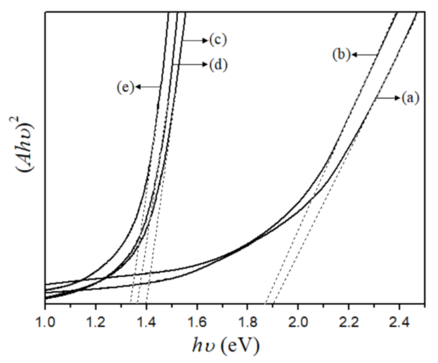
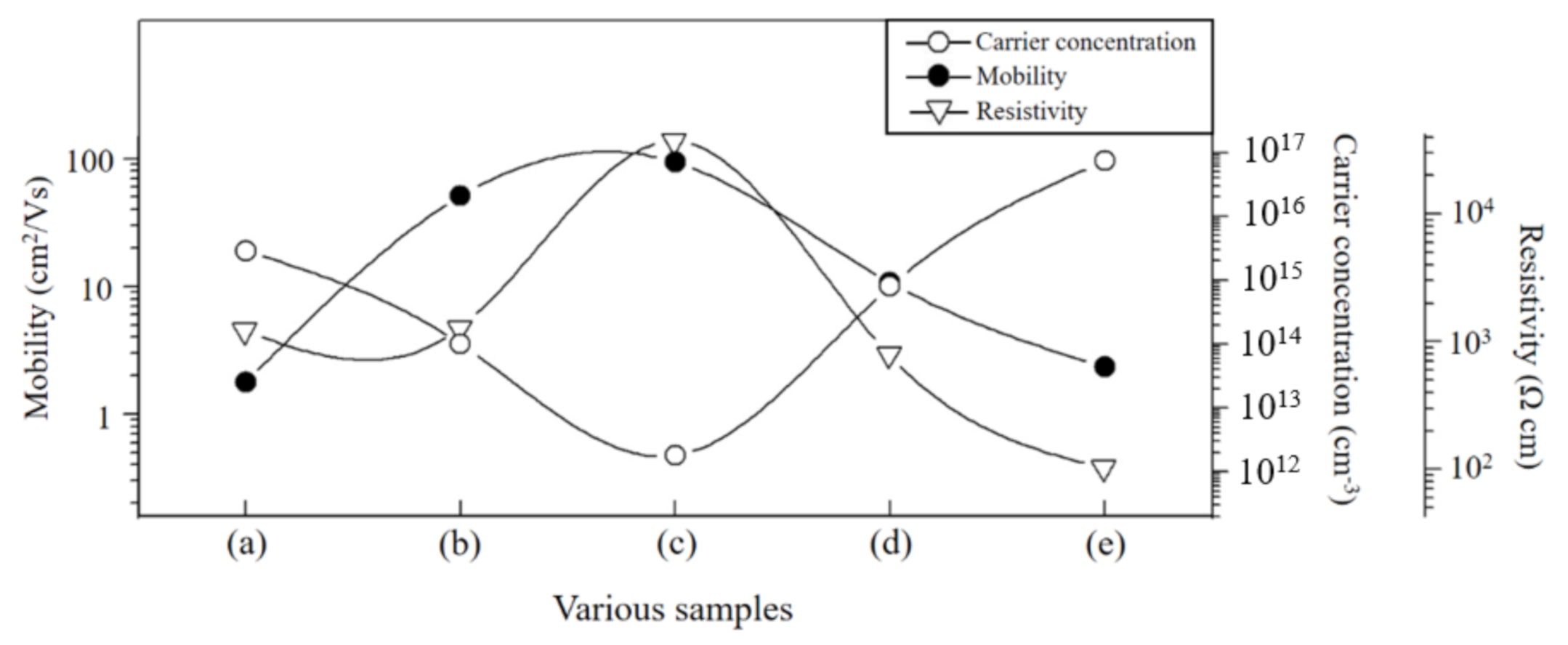
| (a) as-deposited | (Cu2O) | 1.90 | 1.22 × 10³ | 2.9 × 10¹⁵ | 1.8 |
| (b) 200 °C-1 h annealed | (Cu2O) | 1.87 | 1.27 × 10³ | 1.0 × 10¹⁴ | 51.1 |
| (c) 300 °C-1 h annealed | (CuO-Cu2O mixture) | 1.40 | 3.72 × 10⁴ | 1.8 × 10¹² | 93.7 |
| (d) 300 °C-2 h annealed | (CuO) | 1.36 | 7.94 × 10² | 8.0 × 10¹⁴ | 10.7 |
| (e) 300 °C-4 h annealed | (CuO) | 1.34 | 1.02 × 10² | 7.4 × 10¹⁶ | 2.3 |
Publisher’s Note: MDPI stays neutral with regard to jurisdictional claims in published maps and institutional affiliations. |
© 2021 by the authors. Licensee MDPI, Basel, Switzerland. This article is an open access article distributed under the terms and conditions of the Creative Commons Attribution (CC BY) license (https://creativecommons.org/licenses/by/4.0/).
Share and Cite
Lee, W.-J.; Wang, X.-J. Structural, Optical, and Electrical Properties of Copper Oxide Films Grown by the SILAR Method with Post-Annealing. Coatings 2021, 11, 864. https://doi.org/10.3390/coatings11070864
Lee W-J, Wang X-J. Structural, Optical, and Electrical Properties of Copper Oxide Films Grown by the SILAR Method with Post-Annealing. Coatings. 2021; 11(7):864. https://doi.org/10.3390/coatings11070864
Chicago/Turabian StyleLee, Wen-Jen, and Xin-Jin Wang. 2021. "Structural, Optical, and Electrical Properties of Copper Oxide Films Grown by the SILAR Method with Post-Annealing" Coatings 11, no. 7: 864. https://doi.org/10.3390/coatings11070864