Article

Reliable Ohmic Contact Properties for Ni/Hydrogen-Terminated Diamond at Annealing Temperature up to 900 °C

1
Institute for Advanced Materials and Technology, University of Science and Technology Beijing, Beijing 100083, China
2
Research Center for Functional Materials, National Institute for Materials Science (NIMS), 1-1 Namiki, Tsukuba, Ibaraki 305-0044, Japan
3
Research and Services Division of Materials Data and Integrated System, NIMS, 1-1 Namiki, Tsukuba, Ibaraki 305-0044, Japan
*
Authors to whom correspondence should be addressed.
Coatings 2021, 11(4), 470; https://doi.org/10.3390/coatings11040470
Submission received: 23 March 2021 / Revised: 13 April 2021 / Accepted: 13 April 2021 / Published: 17 April 2021
(This article belongs to the Special Issue New Advances in Thin-Film Transistor)

Abstract

:
Ohmic contact with high thermal stability is essential to promote hydrogen-terminated diamond (H-diamond) electronic devices for high-temperature applications. Here, the ohmic contact characteristics of Ni/H-diamond at annealing temperatures up to 900 °C are investigated. The measured current–voltage curves and deduced specific contact resistance (ρC) are used to evaluate the quality of the contact properties. Schottky contacts are formed for the as-received and 300 °C-annealed Ni/H-diamonds. When the annealing temperature is increased to 500 °C, the ohmic contact properties are formed with the ρC of 1.5 × 10⁻³ Ω·cm2 for the Ni/H-diamond. As the annealing temperature rises to 900 °C, the ρC is determined to be as low as 6.0 × 10⁻⁵ Ω·cm2. It is believed that the formation of Ni-related carbides at the Ni/H-diamond interface promotes the decrease in ρC. The Ni metal is extremely promising to be used as the ohmic contact electrode for the H-diamond-based electronic devices at temperature up to 900 °C.

1. Introduction

Diamond, with many remarkable intrinsic properties, possesses vast prospect applications for high-power, high-frequency, and high-temperature electronics [1,2,3]. It exhibits an ultrawide energy bandgap (5.5 eV), high carrier mobilities (4500 and 3800 cm2·V−1·s−1 for electrons and holes, respectively), large breakdown field strength (10 MV·cm−1), and the highest thermal conductivity (22 W cm−1·K−1) [4]. Compared with boron-doped diamond, hydrogen-terminated diamond (H-diamond) shows outstanding p-type surface conductivity with a hole carrier concentration up to ~1014 cm−2 [5,6]. Recently, H-diamond-based field-effect transistors have achieved excellent device performances, such as a high breakdown voltage (2000 V), a high-output current density (1.3 A·mm−1), and a high-output power density (3.8 W·mm−1) [1,7,8]. Meanwhile, the passivation layer protection for the H-diamond surface improves the conductive stability of H-diamond-based electronic devices, even at temperatures as high as 500 °C [9,10,11]. The re-hydrogenation process enables the H-diamond surface damaged during annealing to regain good conductivity [12].
In order to further promote H-diamond-based electronic devices to be operated well at high temperatures, thermal-stable ohmic contact is essential. Until now, different kinds of metals are used for ohmic contacts on the H-diamond, such as, Au, Pd, Pt, W, Ti/Au, Pt/Au, Pd/Ti/Au, Ti/Ni/Au, etc. [12,13,14,15] They show good ohmic contact properties and high thermal stability, with annealing temperatures up to 700 °C. On the other hand, the Ni metal tends to form Schottky contact with the H-diamond at an annealing temperature lower than 100 °C [16]. However, Ni, as a carbophilic element, is prone to react with carbon at an elevated temperature [17]. The solid-solution reaction makes the Ni-related carbides formed at the Ni/H-diamond interface, which would possibly contribute to the formation of ohmic contact.
Here, ohmic contact characteristics of Ni/H-diamond at annealing temperatures up to 900 °C are investigated. The measured current–voltage curves and deduced specific contact resistance (ρC) are used to evaluate the quality of the contact properties.

2. Experimental

2.1. Preparation of H-Diamond Epitaxial Layer

An Ib-type (100) facet single-crystalline diamond was boiled in mixed H2SO4 and HNO3 solutions at 300 °C for 3 h. Then, it was ultrasonically cleaned using acetone, ethanol, and deionized water sequentially. A 150-nm-thick H-diamond epitaxial layer was grown using a microwave plasma-enhanced chemical vapor deposition system. The CH4 flow rate, H2 flow rate, chamber pressure, and deposition temperature were 0.5 sccm, 500 sccm, 80 Torr, and 900–940 °C, respectively.

2.2. Formation of Transmission Line Model (TLM) Patterns for Ni on the H-Diamond

The H-diamond was sequentially coated with LOR5A and AZ5214E positive photoresists using a spin-coater with a rotation rate and time of 7000 rpm and 1 s, respectively. After exposing using a mask-less lithography system with a dose energy of 250 mJ·cm−2, the sample was developed in a 2.38% tetramethylammonium hydroxide solution for 90 s. The Ti metal used as key-patterns was deposited on the H-diamond by a J-sputter system in an Ar atmosphere in order to align the positions of the mesa structure and contact metals. The mesa structure was formed using a capacitively coupled plasma reactive-ion etching system. The plasma power, O2 flow rate, and etching time were 50 W, 100 sccm, and 90 s, respectively. The five-group TLM electrode patterns were completed using the lithography procedures. The Ni, with a thickness of 100 nm, was grown on the H-diamond for ohmic contact via an e-beam evaporation system under a ~10−5 Pa vacuum condition.

2.3. Annealing Process and Current–Voltage Measurements

The annealing process was performed using a rapid thermal annealing system in an Ar atmosphere. The annealing temperatures were 300, 500, 700, and 900 °C with an annealing time of 10 min for each temperature. After annealing, the sample was exposed to air for more than 10 h in order to promote the formation of a negatively adsorbed layer on the surface of the H-diamond, and to regain good surface conductivity. The calculations of ρC for the Ni/H-diamond with the TLM patterns can be referred to in the previous reports [18,19]. The electrical properties of Ni/H-diamond contacts were characterized by a room-temperature probe system.

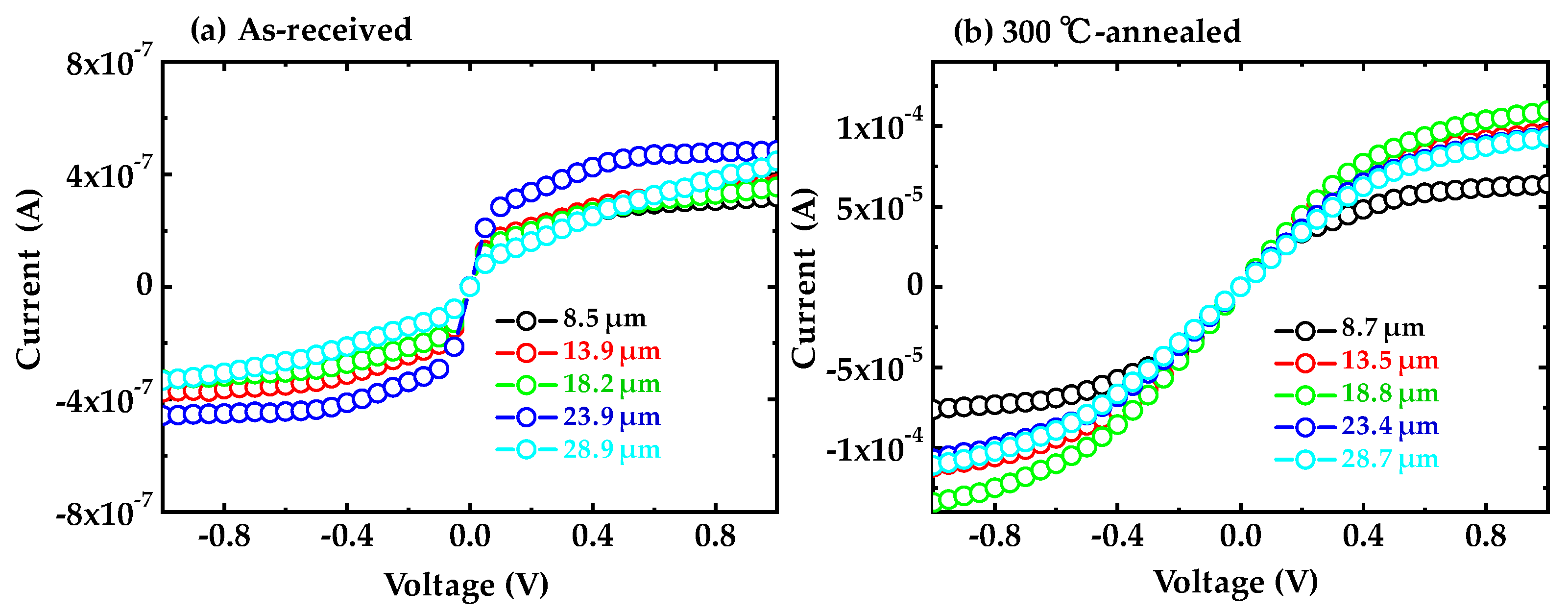
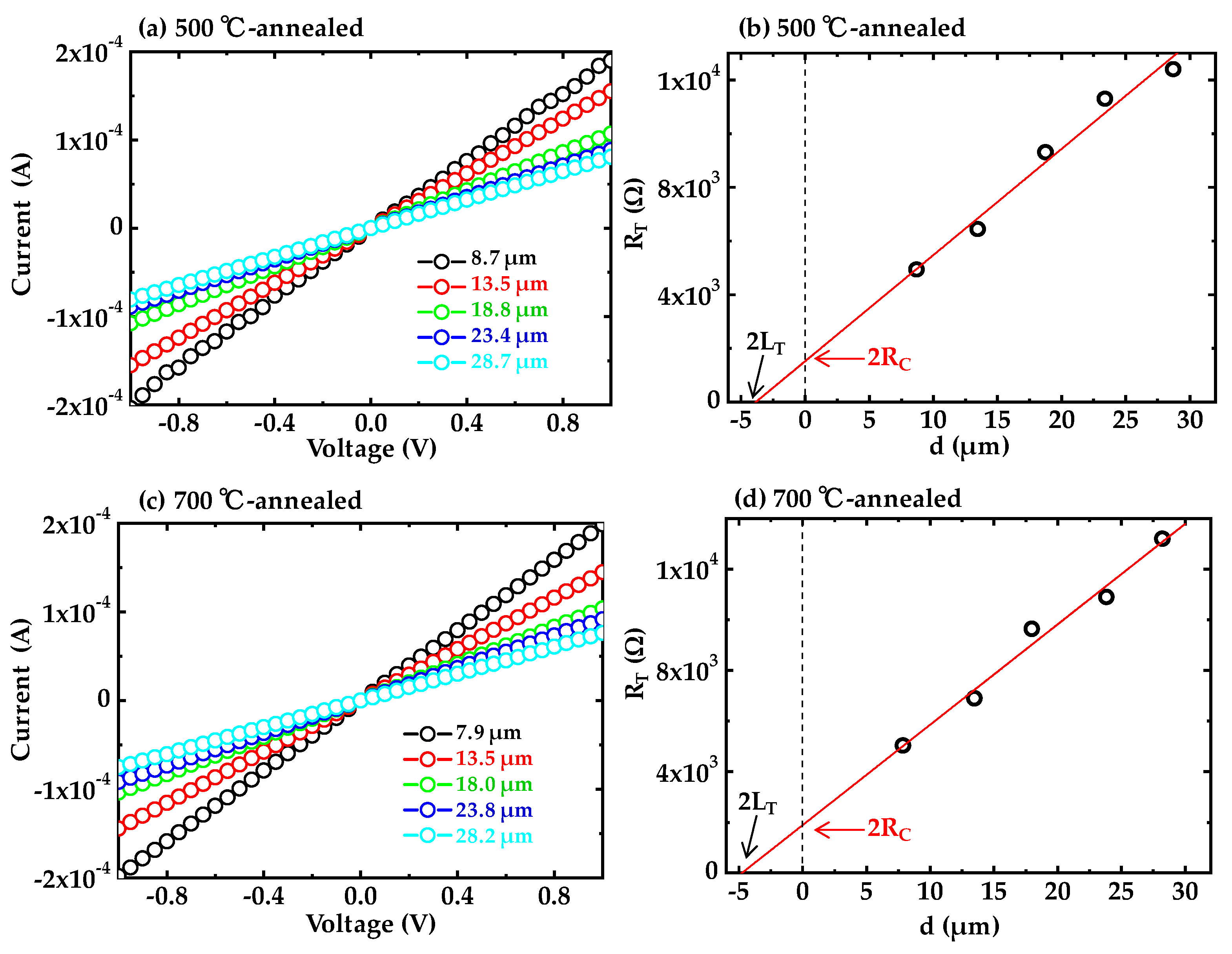
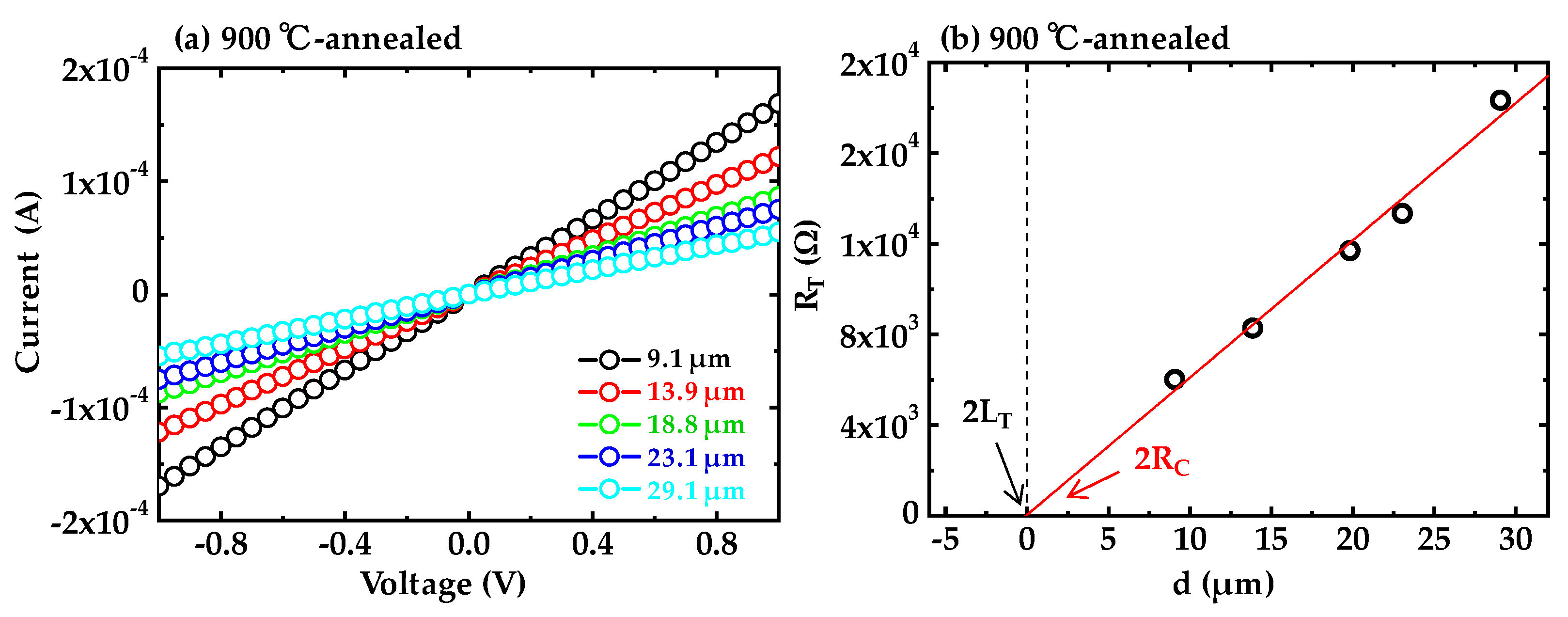
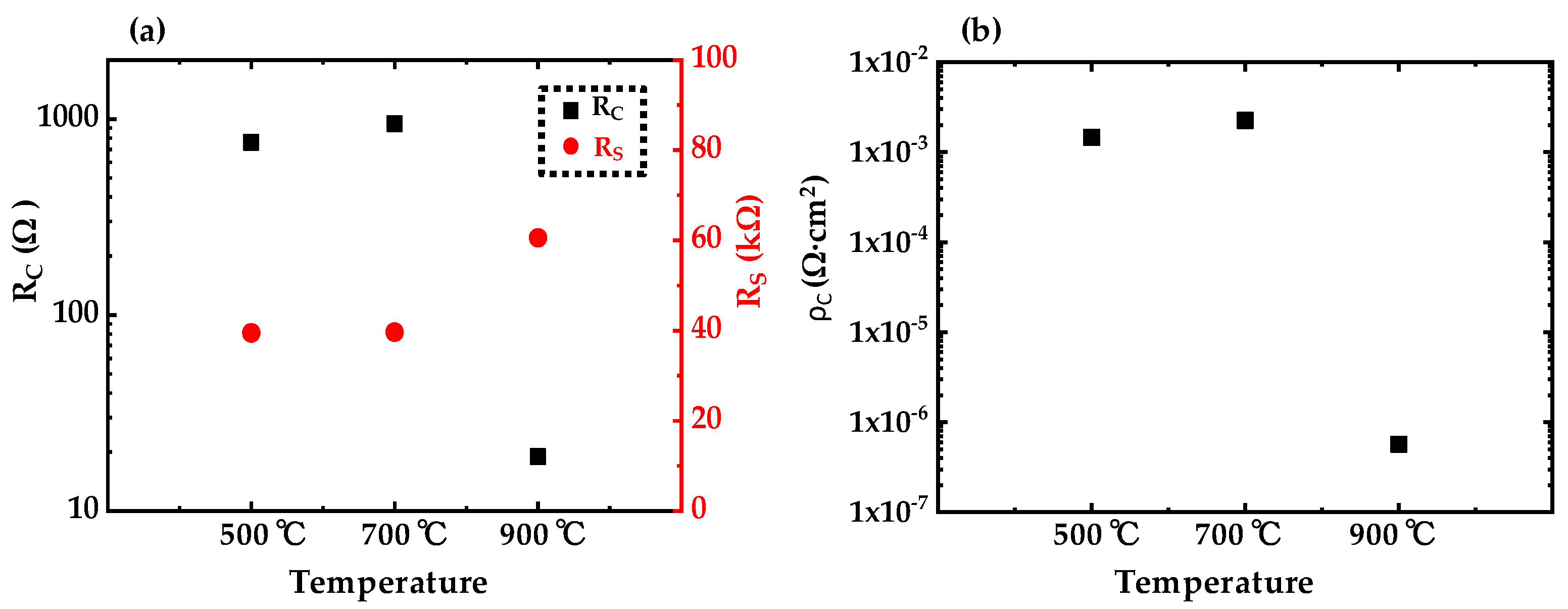
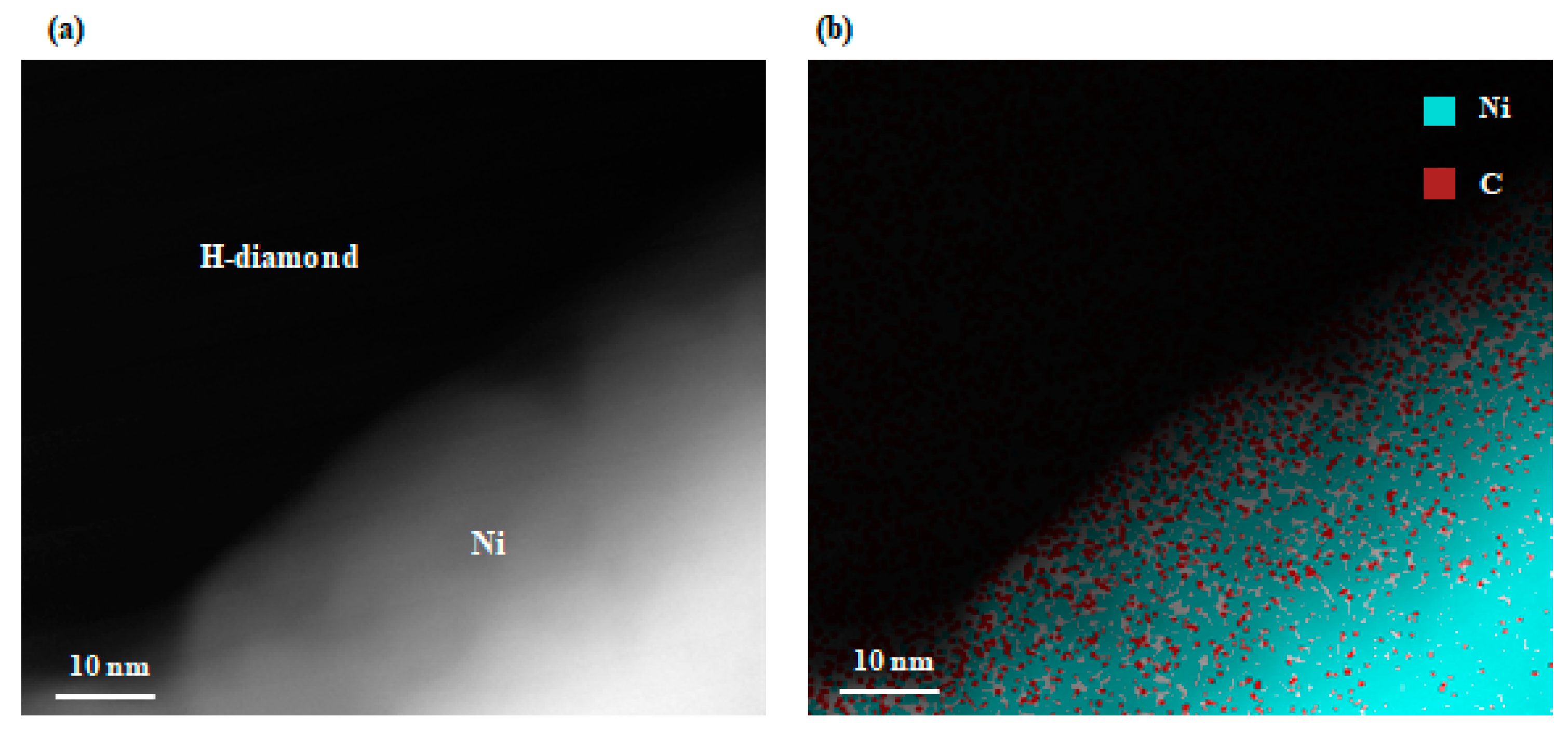
3. Results and Discussion

Figure 1 shows the surface morphology of five-group TLM patterns of Ni on the H-diamond epitaxial layer before annealing. The length and width of each electrode are the same as 100 μm. All the Ni metals were stable to be formed on the H-diamond. The five groups of TLM patterns were used to characterize current–voltage curves for the Ni/H-diamonds of as-received, 300 °C-annealed, 500 °C-annealed, 700 °C-annealed, and 900 °C-annealed, respectively. The interspace (d) values from left to right in Figure 1, between the two adjacent electrodes for the five-group TLM patterns, are in the ranges of 7.9–9.1 μm, 13.5–13.9 μm, 18.0–18.8 μm, 23.1–23.9 μm and 28.2–29.1 μm, respectively.
Figure 2 shows current–voltage characteristics of (a) the as-received and (b) the 300 °C -annealed Ni/H-diamond contacts, respectively. The applied voltage is in the range of –1.0–1.0 V. For the as-received Ni/H-diamond contact, the output currents are in the order of 10−7 A (Figure 2a). All the curves show non-linear characteristics, indicating the Schottky contacts. After annealing at 300 °C for 10 min, as shown in Figure 2b, the output currents of the Ni/H-diamond increase to the order of 10−4 A. The annealing process improves the contact properties of the Ni/H-diamond. However, all the curves still show non-linear characteristics. Therefore, even after annealing at 300 °C, the Ni/H-diamond still operates with Schottky contacts, which is consistent with the results obtained from the other report [20]. The presence of a chemisorbed species on the H-diamond surface possibly results in the formation of Schottky contact. However, the annealing process can improve the contact interface of the Ni/H-diamond, thereby promoting the current flow.
Figure 3a shows the current–voltage characteristics of the Ni/H-diamond after annealing at 500 °C. All the current–voltage curves have linear characteristics, which implies good ohmic contacts for the Ni/H-diamond. For two adjacent electrodes in which d = 8.7 μm, the output currents are 2.0 × 10⁻⁴ A at ±1.0 V. The total resistance (RT) for the 500 °C-annealed Ni/H-diamond can be calculated to be 4.9 × 10³ Ω (d = 8.7 μm). Based on the current–voltage characteristics for other adjacent electrodes (Figure 3a), the RT for the Ni/H-diamond with other d values is also calculated and summarized in Figure 3b. There are the following relationships for the RT and ρC with the Ni/H-diamond contact resistance (RC), H-diamond surface sheet resistance (RS), electrode transfer length (LT), and electrode width (W) [18]:
R T = 2 R C + R s W d
ρ C = R C × L T × W
By fitting the spots in Figure 3b, the RS/W (the slope of fitting line) are determined to be 4.0 × 10² Ω·μm−1 with an RS of 40 kΩ. The 2RC (the intercept of the y-axis) and 2LT (the intercept of the x-axis) are deduced to be 1.5 × 10³ Ω and 3.9 μm, respectively. Based on Equation (2), the ρC for the 500 °C-annealed Ni/H-diamond can be calculated to be 1.5 × 10⁻³ Ω·cm2.
When the annealing temperature is increased to 700 °C, the output current maxima are the same level as those of the 500 °C-annealed Ni/H-diamond (Figure 3c). The linear characteristics for all the current–voltage curves are observed, indicating the good ohmic properties for the 700 °C-annealed Ni/H-diamond. Figure 3d shows the RT as a function of d for the Ni/H-diamond after annealing at 700 °C. By fitting the spots, the RS/W, 2RC, and 2LT are obtained to be 4.0 × 10² Ω·μm−1, 1.9 × 10³ Ω, and 4.8 μm, respectively. The RS and ρC for the Ni/H-diamond after annealing at 700 °C are calculated to be 40 kΩ and 2.3 × 10⁻³ Ω·cm2, respectively, which are close to those of the 500 °C-annealed Ni/H-diamond.
Figure 4a shows the current-voltage curves of the Ni/H-diamond after annealing at 900 °C. All the curves have good linear relationships. Therefore, the ohmic contacts of the Ni/H-diamond possess good thermal stability even after annealing at temperatures as high as 900 °C for 10 min, which is comparable with those of the Ni/SiC contacts [21,22].
Comparing with the output currents of the 500 °C-annealed and 700 °C-annealed Ni/H-diamonds at ±1.0 V, those for the 900 °C-annealed one decreased slightly. Figure 4b shows the corresponding RT as a function of d for the Ni/H-diamond after annealing at 900 °C. The RS/W, 2RC, and LT are deduced to be 6.1 × 10² Ω·μm−1, 37.9 Ω, and 0.1 μm, respectively. The RS and ρC are calculated to be 60.6 kΩ and 6.0 × 10⁻⁵ Ω·cm2. The ρC is comparable with other metals on the H-diamond [23,24]. The thermal-stable Ni/H-diamond ohmic contacts exhibit advantages for the high-temperature application of H-diamond-based devices.
Figure 5a,b compare the RC, RS and ρC of the Ni/H-diamonds after annealing at 500, 700, and 900 °C, respectively. After annealing at 500 and 700 °C, the RC and RS values of the Ni/H-diamonds show no obvious changes. After annealing at 900 °C, however, the RC decreases to 19.0 Ω, while the RS increases to 60.6 kΩ. The increased RS is possibly attributed to the damage of C–H bonds or the desorbed absorption layer on the H-diamond surface after multiplied high-temperature treatments [5]. The decrease in RC may be due to the carbon phase transition at the interface between Ni and H-diamond at high temperatures [24,25]. Under the catalysis of nickel, diamond is prone to transform into the graphite phase or form carbide related with Ni, which greatly increases the electrical conductivity, thereby greatly reducing the contact resistance at the interface.
In order to confirm the interface reaction between Ni and H-diamond after annealing, transmission electron microscope (TEM) (Figure 6a) and energy dispersive spectrometer (EDS) (Figure 6b) measurements for the Ni/H-diamond after annealing were performed. The interface for the Ni/H-diamond is ambiguous and curved after annealing. The EDS result shows a great number of carbon atoms from diamond dissolved into the Ni lattice. Therefore, the carbides related with Ni for the Ni/H-diamond are formed at the interface, which leads to a lower ρC.

4. Conclusions

In this study, ohmic contact characteristics of the Ni/H-diamond at annealing temperatures up to 900 °C were investigated. Schottky contacts were formed for the as-received and the 300 °C-annealed Ni/H-diamonds. When the annealing temperatures were increased to 500 °C, ohmic contacts were formed with the ρC of 1.5 × 10⁻³ Ω·cm2 for the Ni/H-diamond. For the 700 °C-annealed Ni/H-diamond, the ρC was the same level as that of the 500 °C-annealed one. As the annealing temperature rose to 900 °C, the specific contact resistance was as low as 6.0 × 10⁻⁵ Ω·cm2. It is believed that the formation of Ni-related carbides at the Ni/H-diamond interface promoted the decrease in specific contact resistance. Therefore, the thermal-stable Ni/H-diamond ohmic contacts exhibited advantages for the high-temperature application of H-diamond-based devices.

Author Contributions

Conceptualization, J.L. (Jiangwei Liu); methodology, X.Y. and J.L. (Jiangwei Liu); validation, X.Y., J.L. (Jinlong Liu), and J.W.; formal analysis, X.Y. and B.D.; investigation, X.Y. and J.L. (Jiangwei Liu); resources, J.L. (Jiangwei Liu), C.L. and Y.K.; data curation, X.Y. and J.L. (Jiangwei Liu); writing—original draft preparation, X.Y.; writing—review and editing, J.L. (Jiangwei Liu); supervision, J.L. (Jiangwei Liu) and C.L.; funding acquisition, J.L. (Jiangwei Liu) Y.K., and C.L. All authors have read and agreed to the published version of the manuscript.

Funding

This work is supported partly by the Leading Initiative for Excellent Young Researchers Program Project, the KAKENHI Project under grant numbers of JP20H00313 and JP16H06419, and the NIMS Nanofabrication Platform of the Nanotechnology Platform Project sponsored by the Ministry of Education, Culture, Sports, and Technology, Japan. It is supported partly by the National Key Research and Development Program of China (No. 2016YFE0133200).

Institutional Review Board Statement

Not applicable.

Informed Consent Statement

Not applicable.

Data Availability Statement

The data presented in this study are available on request from the corresponding author.

Conflicts of Interest

The authors declare no conflict of interest.

References

  1. Imanishi, S.; Horikawa, K.; Oi, N.; Okubo, S.; Kageura, T.; Hiraiwa, A.; Kawarada, H. 3.8W/mm RF power density for ALD Al2O3-based two-dimensional hole gas diamond mosfet operating at saturation velocity. IEEE Electron. Device Lett. 2019, 40, 279–282. [Google Scholar] [CrossRef]
  2. Anniyev, T.; Vasilyev, M.; Khabashesku, V.; Inanc, F. High-temperature diamond detector for neutron generator output monitoring in well logging applications. IEEE Trans. Nucl. Sci. 2020, 67, 1885–1892. [Google Scholar] [CrossRef]
  3. Yu, X.X.; Zhou, J.J.; Qi, C.J.; Cao, Z.Y.; Kong, Y.C.; Chen, T.S. A High frequency hydrogen-terminated diamond MISFET with fT/fmax of 70/80 GHz. IEEE Electron. Device Lett. 2018, 39, 1373–1376. [Google Scholar] [CrossRef]
  4. Wort, C.J.H.; Balmer, R.S. Diamond as an electronic material. Mater. Today 2008, 11, 22–28. [Google Scholar] [CrossRef]
  5. Williams, O.A.; Jackman, R.B. Surface conductivity on hydrogen terminated diamond. Semicond. Sci. Technol. 2003, 18, S34–S40. [Google Scholar] [CrossRef]
  6. Kubovic, M.; Kasu, M. Improvement of hydrogen-terminated diamond field effect transistors in nitrogen dioxide atmosphere. Appl. Phys. Express 2009, 2, 086502. [Google Scholar] [CrossRef]
  7. Hirama, K.; Sato, H.; Harada, Y.; Yamamoto, H.; Kasu, M. Diamond field-effect transistors with 1.3 A/mm drain current density by Al2O3 passivation Layer. Jpn. J. Appl. Phys. 2012, 51, 090112. [Google Scholar]
  8. Kitabayashi, Y.; Kudo, T.; Tsuboi, H.; Yamada, T.; Xu, D.; Shibata, M.; Matsumura, D.; Hayashi, Y.; Syamsul, M.; Inaba, M.; et al. Normally-off C–H diamond MOSFETs with partial C–O channel achieving 2-kV breakdown voltage. IEEE Electron. Device Lett. 2017, 38, 363–366. [Google Scholar] [CrossRef]
  9. Kawarada, H.; Tsuboi, H.; Naruo, T.; Yamada, T.; Xu, D.; Daicho, A.; Saito, T.; Hiraiwa, A. C–H surface diamond field effect transistors for high temperature (400 °C) and high voltage (500 V) operation. Appl. Phys. Lett. 2014, 105, 013510. [Google Scholar] [CrossRef]
  10. Liu, J.W.; Oosato, H.; Da, B.; Teraji, T.; Kobayashi, A.; Fujioka, H.; Koide, Y. Operations of hydrogenated diamond metal-oxide-semiconductor field-effect transistors after annealing at 500 °C. J. Phys. D Appl. Phys. 2019, 52, 315104. [Google Scholar] [CrossRef]
  11. Ren, Z.Y.; Yuan, G.S.; Zhang, J.F.; Xu, L.; Zhang, J.C.; Chen, W.J.; Hao, Y. Hydrogen-terminated polycrystalline diamond MOSFETs with Al2O3 passivation layers grown by atomic layer deposition at different temperatures. AIP Adv. 2018, 8, 065026. [Google Scholar] [CrossRef]
  12. Vardi, A.; Tordjman, M.; Kalish, R.; Alamo, J.A.d. Refractory W Ohmic contacts to H-terminated diamond. IEEE Trans. Electron. Devices 2020, 67, 3516–3521. [Google Scholar] [CrossRef]
  13. Xing, K.J.; Tsai, A.; Rubanov, S.; Creedon, D.L.; Yianni, S.A.; Zhang, L.; Hao, W.C.; Zhuang, J.C.; McCallum, J.C.; Pakes, C.I.; et al. Palladium forms Ohmic contact on hydrogen-terminated diamond down to 4 K. Appl. Phys. Lett. 2020, 116, 111601. [Google Scholar] [CrossRef]
  14. Zhang, M.H.; Lin, F.; Wang, W.; Li, F.N.; Wang, Y.F.; Abbasi, H.N.; Zhao, D.; Chen, G.Q.; Wen, F.; Zhang, J.W.; et al. Ohmic contact of Pt/Au on hydrogen-terminated single crystal diamond. Coatings 2019, 9, 539. [Google Scholar] [CrossRef] [Green Version]
  15. Umezawa, H.; Ikeda, K.; Kumaresan, R.; Shikata, S. High temperature characteristics of diamond SBDs. Mater. Sci. Forum 2010, 645, 1231–1234. [Google Scholar] [CrossRef]
  16. Tsugawa, K.; Noda, H.; Hirose, K.; Kawarada, H. Schottky barrier heights, carrier density, and negative electron affinity of hydrogen-terminated diamond. Phys. Rev. B 2010, 81, 045303. [Google Scholar] [CrossRef]
  17. Chen, J. Research on Catalytic Etching of Synthetic Diamond by Iron Group Metals. Master’s Thesis, Hunan University, Changsha, China, 2015. [Google Scholar]
  18. Reeves, G.K.; Harrison, H.B. Obtaining the specific contact resistance from transmission line model measurements. IEEE Electron. Device Lett. 1982, 3, 111–113. [Google Scholar] [CrossRef]
  19. Berger, H.H. Models for contacts to planar devices. Solid State Electron. 1972, 15, 145–158. [Google Scholar] [CrossRef]
  20. Weide, J.; Nemanich, R.J. Influence of interfacial hydrogen and oxygen on the Schottky barrier height of nickel on (111) and (100) diamond surfaces. Phys. Rev. B 1994, 49, 13629–13637. [Google Scholar] [CrossRef]
  21. Roccaforte, F.; La Via, F.; Raineri, V.; Calcagno, L.; Musumeci, P. Improvement of high temperature stability of nickel contacts on n-type 6H–SiC. Appl. Surf. Sci. 2001, 184, 295–298. [Google Scholar] [CrossRef]
  22. Chang, S.K.; Kim, Y.; Lee, J.; Choi, K. Thermal stability study of Ni–Si silicide films on Ni/4H-SiC contact by in-situ temperature-dependent sheet resistance measurement. Jpn. J. Appl. Phys. 2019, 58, 075503. [Google Scholar] [CrossRef]
  23. Yuan, X.L.; Liu, J.W.; Shao, S.W.; Liu, J.L.; Wei, J.J.; Da, B.; Li, C.M.; Koide, Y. Thermal stability investigation for Ohmic contact properties of Pt, Au, and Pd electrodes on the same hydrogen-terminated diamond. Aip Adv. 2020, 10, 055114. [Google Scholar] [CrossRef]
  24. Zhang, P.F.; Zhang, S.P.; Chen, W.D.; Yan, S.F.; Ma, W.; Wang, H.X. Annealing temperature on contact properties between nickel film and hydrogen-terminated single crystal diamond. Coatings 2020, 10, 876. [Google Scholar] [CrossRef]
  25. Kanada, S.; Nagai, M.; Ito, S.; Matsumoto, T.; Ogura, M.; Takeuchi, D.; Yamasaki, S.; Inokuma, T.; Tokuda, N. Fabrication of graphene on atomically flat diamond (111) surfaces using nickel as a catalyst. Diam. Relat. Mater. 2017, 75, 105–109. [Google Scholar] [CrossRef]
Figure 1. Surface morphology of the five-group transmission line model (TLM) patterns of Ni on the hydrogen-terminated diamond (H-diamond) epitaxial layer before annealing. They were used to characterize current–voltage curves for the Ni/H-diamonds of as-received, 300 °C-annealed, 500 °C-annealed, 700 °C-annealed, and 900 °C-annealed, respectively.
Coatings 11 00470 g001
Figure 2. Current–voltage characteristics of (a) the as-received and (b) the 300 °C-annealed Ni/H-diamond contacts, respectively.
Coatings 11 00470 g002
Figure 3. (a,c) Current–voltage characteristics of the 500 °C-annealed and 700 °C-annealed Ni/H-diamonds, respectively. (b,d) RT as functions of d for the 500 °C-annealed and 700 °C-annealed Ni/H-diamonds, respectively.
Coatings 11 00470 g003
Figure 4. (a) Current–voltage characteristics and (b) total resistance (RT) as functions of d for the 900 °C-annealed Ni/H-diamond.
Coatings 11 00470 g004
Figure 5. Summary of (a) the contact resistance (RC) and surface sheet resistance (RS), and (b) the deduced specific contact resistance (ρC) for the Ni/H-diamond after annealing at 500, 700, and 900 °C, respectively.
Coatings 11 00470 g005
Figure 6. (a) Transmission electron microscope (TEM) and (b) energy dispersive spectrometer (EDS) images for the interface of the Ni/H-diamond after annealing at 900 °C, respectively.
Coatings 11 00470 g006
Publisher’s Note: MDPI stays neutral with regard to jurisdictional claims in published maps and institutional affiliations.

