1. Introduction
In general, the thin film deposition mechanism is explained by the terrace–ledge–kink (TLK) model [
1,
2,
3,
4]. In the TLK model, an atom adsorbed on the terrace diffuses to the monoatomic ledge and is incorporated into the crystal at a kink. However, some deposition behaviors of thin films that are difficult to explain based on the TLK model were observed [
5,
6,
7,
8,
9]. In order to explain such puzzling behavior, the concept of the two-step growth or non-classical crystallization was suggested [
10,
11,
12,
13]. In this new concept, the building block for crystal growth is not an individual atom but a nanoparticle formed in the solution or in the gas phase.
Recently, non-classical crystallization has been studied extensively. Thanks to the development of advanced measurement techniques, direct observations of non-classical crystallization by transmission electron microscopy (TEM) using a liquid cell technique have been reported in many systems [
14,
15,
16]. Several review papers and a few books on non-classical crystallization have been published and its tutorial and technical sessions were included at the international conference [
10,
11,
12,
17].
In relation to non-classical crystallization in the gas phase synthesis of films, Hwang et al. [
7,
18,
19,
20,
21,
22] suggested a theory of charged nanoparticles (TCN), where electrically charged nanoparticles (CNPs) are spontaneously formed in the gas phase and these CNPs become a building block of thin films [
7,
18,
19,
20,
21,
22]. They emphasized that the size of CNPs and the electric charge carried by the CNPs play a critical role in the evolution of dense films. In addition, this new growth mechanism was studied in various deposition processes such as atmospheric pressure chemical vapor deposition (APCVD) [
23,
24,
25,
26], hot wire CVD (HWCVD) [
5,
6,
7,
9,
21,
27,
28], plasma enhanced CVD (PECVD) [
20,
22,
29,
30], and sputtering [
31,
32,
33]. According to this theory, the deposition behavior of nanoparticles changes drastically, depending on whether or not the nanoparticles are charged. If the nanoparticles are neutral, they will undergo random Brownian coagulation and produce a porous thin film. If they are charged, however, a dense thin film will be deposited by self-assembly and liquid-like coalescence of CNPs. In other words, if the nanoparticles are small enough, the presence of a charge makes the nanoparticles liquid-like. When the nanoparticles are charged, the binding force between atoms is weakened, resulting in liquid-like properties. The relationship between charging and weakening of binding force is reported by Clare’s ab-initio calculation of the bond strength between Si–Si and Si–H of silane (SiH
4) and disilane (Si
2H
6) molecules with or without charge [
34].
Recently, Jang et al. [
35] and Kim et al. [
36] showed that during the thin film deposition by Radio Frequency (RF) and Direct Current (DC) magnetron sputtering, respectively, both neutral and charged nanoparticles were generated with the ratio of neutral and charged nanoparticles affected by the processing conditions such as pressure and plasma power. According to the TCN, in order to deposit a dense film, the size of nanoparticles generated in the gas phase must be small and have a charge. It was shown that nanoparticles tend to be charged by contact charging under the condition where no additional effort was made to charge nanoparticles. From the perspective of TCN, in most CVD processes, CNPs are generated in the gas phase and films are grown on the substrate by their building blocks.
On the other hand, there is a process for synthesizing the nanoparticles rather than thin films using the system similar to CVD. It is called a chemical vapor condensation (CVC) system, where the precursor is decomposed at a high temperature to create clusters or nanoparticles in the gas phase [
37]. The nanoparticles then condense out on a rotating liquid N
2 cooled substrate from which the particles can be scraped off and collected. Considering the two-step growth of thin films by the TCN, nanoparticles formed in the CVC process can be deposited as a film on the substrate at a low temperature.
Although the TCN showed that most films in the CVD process are deposited by the charged nanoparticles generated in the gas phase, which is identical with the two-step growth, no attempt has been made to use the two-step growth in order to achieve the low temperature deposition.
The purpose of this study is to check the possibility of the film deposition by nanoparticles generated in the gas phase using a two-chamber system similar to the CVC process and to find out the optimum condition to deposit a dense film.
2. Materials and Methods
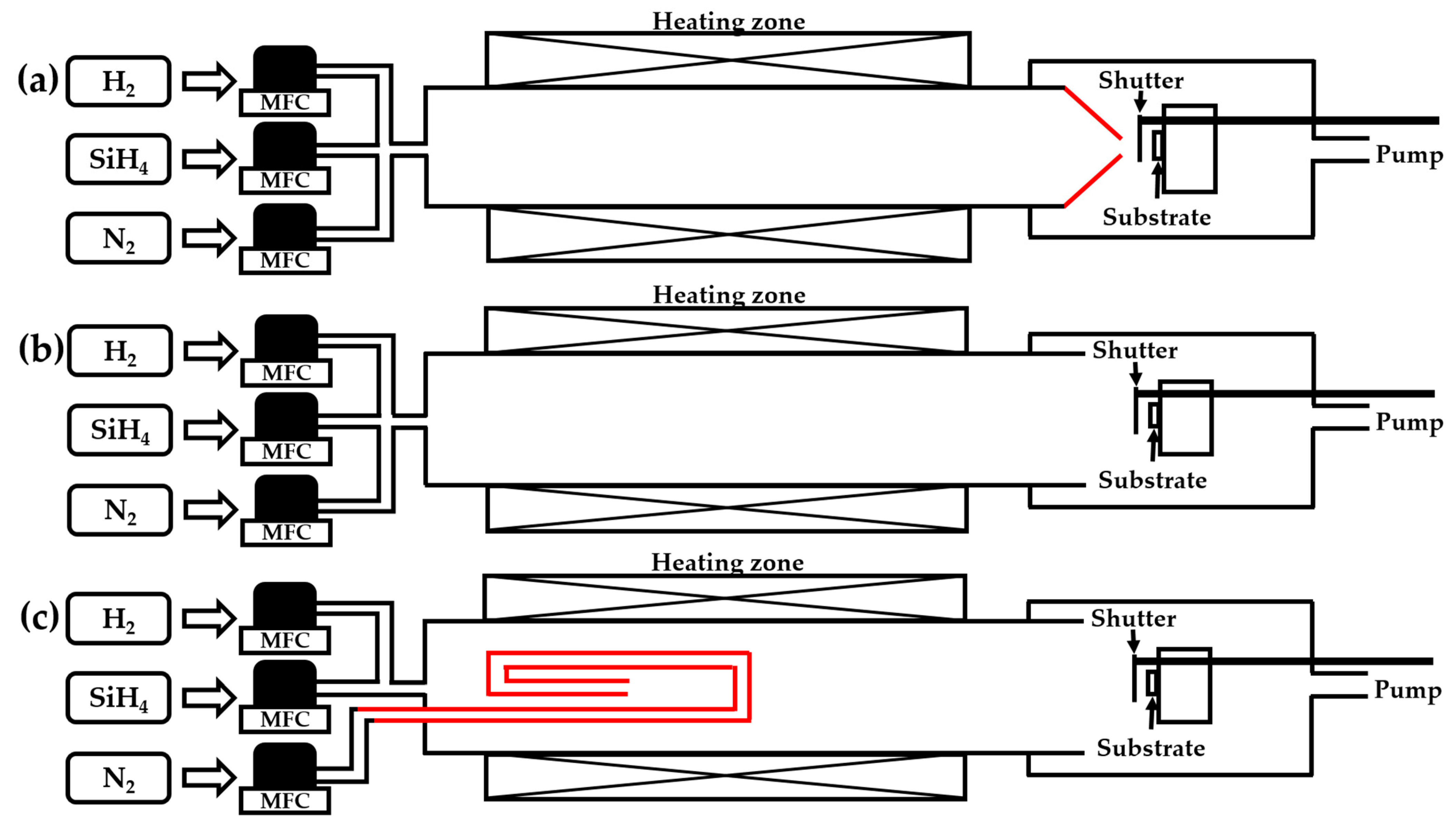
The experimental setup is schematically shown in
Figure 1. It consisted of a thermal tube furnace and a low pressure chamber. The tube furnace was heated to decompose SiH
4 at 1100 °C and to generate silicon oxide nanoparticles in the gas phase. Silicon oxide nanoparticles were carried to the second chamber to deposit on the substrate. The second chamber was evacuated by the rotary pump to the base pressure of approximately 40 mTorr for 2 h. The shutter, which covered the substrate as shown in the right of
Figure 1, was used to capture the nanoparticles using the delay time. The delay time means the amount of time during which the substrate was covered by the shutter. The reason to install the shutter is to prevent the deposition of nanoparticles on the substrate during the delay time.
Helium (He) diluted with 10 vol.% SiH
4 of 99.9999% purity was used as a precursor and H
2 of 99.9999% purity and N
2 of 99.9999% were used as carrier gases. The gas mixture of 10% SiH
4–90% He was supplied at 5 standard cubic centimeters per min (sccm). At the same time, H
2 was supplied at 50 sccm. The flow rate of N
2 varied according to the experiment. The flow rate of each gas was controlled by a mass flow controller (MFC). The gas supply system is shown at the left of
Figure 1.
At the outlet of the quartz tube with the conical nozzle shown in
Figure 1a, the gases and the synthesized nanoparticles were accelerated much faster than the nanoparticles coming out through the quartz tube without the nozzle as shown in
Figure 1b. Due to this flux, the substrate, which was initially at room temperature, was heated to ~170 °C. By this scheme, the two-step deposition can be achieved, where the precursor was decomposed at 1100 °C in the hot zone of the tube furnace and the films can be deposited on the substrate at ~170 °C.
In order to obtain dense films using this two-step deposition, the growth of nanoparticles generated in the hot zone of the tube furnace should be minimized until they reached the substrate in the second chamber. In order to find out the optimum condition, we varied the flow rate of N2 and the nozzle diameter. We also tested the quartz tube without a nozzle and tried preheating of N2 as follows.
In the first set of deposition, the diameter of the conical nozzle of the quartz tube was fixed as 10 mm as schematically shown in
Figure 1a and the flow rate of N
2 was varied as 0, 50, 500, 5000, 15,000, and 25,000 sccm. In the second set of deposition, the flow rate of N
2 was fixed as 5000 sccm and the diameter of the quartz nozzle was varied as 5, 10, 15, and 20 mm. In the third set, the flow rate of N
2 was fixed as 5000 sccm and the quartz tube had no nozzle as shown in
Figure 1b. When there is a nozzle at the right end of the quartz tube as shown in
Figure 1a, the gases and nanoparticles would be accelerated in the gas phase. When there is no nozzle at the right end of the quartz tube as shown in
Figure 1b, however, gases and nanoparticles would flow out of the tube without being accelerated. In the fourth set, the deposition condition was the same as that of the third set except that N
2 was preheated as shown in
Figure 1c. N
2 was made to flow through the stainless tube with a diameter of 0.63 cm, which was extended to the maximum temperature zone and the outlet of the tube was located at the region, where the precursor gas was supplied inside the tube furnace. Therefore, N
2 passed through the highest temperature zone of 1100 °C and would heat the precursor near the outlet of the stainless tube.
The thin films were deposited on a 10 mm × 10 mm × 1 mm p-type Si (100) substrate for 1 h. The distance between the end of the quartz tube and the substrate was 1 cm. For deposition of films, a silicon substrate was placed on a quartz plate of 1 mm thickness. The top view and cross section of the films were observed by field emission scanning electron microscopy (FESEM, SU-70, Hitachi, Tokyo, Japan). In order to check how the size of the nanoparticles formed in the gas phase changed with time, nanoparticles were captured for 10 s on the carbon membrane with delay times of 0, 2, 7, 30 min, which was counted after the precursor gas was supplied. For capturing silicon oxide nanoparticles, a pure carbon TEM membrane was placed on the quartz plate. The silicon oxide nanoparticles captured on a carbon membrane were observed by transmission electron microscopy (TEM, Tecnai F20, Hillsboro, OR, USA). The open source software ImageJ (1.51k, National Institutes of Health, Bethesda, MD, USA) was used to analyze the size distribution of nanoparticles of TEM images.
3. Results and Discussion
Figure 2 shows the FESEM images of the cross section of silicon oxide films deposited on the substrate with varying flow rates of N
2. At the flow rate of 0, 50 and 500 sccm of N
2, the film was hardly formed, only partially covering the substrate as shown in
Figure 2a–c, respectively. At the flow rate of 5000 sccm, an appreciable amount of silicon oxide was deposited, forming the continuous film as shown in
Figure 2d. As the flow rate was further increased to 15,000 sccm, however, the film growth rate was decreased pronouncedly as shown in
Figure 2e. At the flow rate of 25,000 sccm, the continuous film was not formed as shown in
Figure 2f.
This result indicates that although the flow rate of the SiH
4 precursor was the same, the deposition behavior of nanoparticles was affected markedly by the flow rate of the N
2 carrier gas. As to why in
Figure 2a–c, the film was hardly deposited at the flow rate of 0, 50, and 500 sccm of N
2, one possibility we could think of is that the flux of nanoparticles spread out after the nozzle instead of focusing on the substrate because of the low N
2 flow rate. It appeared that the flux of nanoparticles focused on the substrate at the flow rate of 5000 sccm, producing a film of appreciable thickness. As to the reason why the deposited flux decreased with further increasing flow rate of N
2 as shown in
Figure 2e,f, the SiH
4 precursor would not be decomposed fully as the residence time decreased with increasing flow rate.
Since the deposited flux was maximum at the N
2 flow rate of 5000 sccm, the flow rate was fixed as 5000 sccm and the diameter of the nozzle at the end of the quartz tube was varied as 5, 10, 15, and 20 mm for the two-step deposition.
Figure 3 shows the FESEM images of the top view and cross section of the deposited films.
Figure 3a–d show the top view of the deposition, respectively, at the nozzle diameters of 5, 10, 15 and 20 mm with
Figure 3e–h showing, respectively, the cross section of the deposition.
The growth rate was maximum for the film deposited at the nozzle diameter of 5 mm and tended to decrease with increasing diameter as shown in
Figure 3. However, the size of nanoparticles tended to be too large, resulting in a rough and porous structure, which was clearly revealed in
Figure 3c,d,g,h.
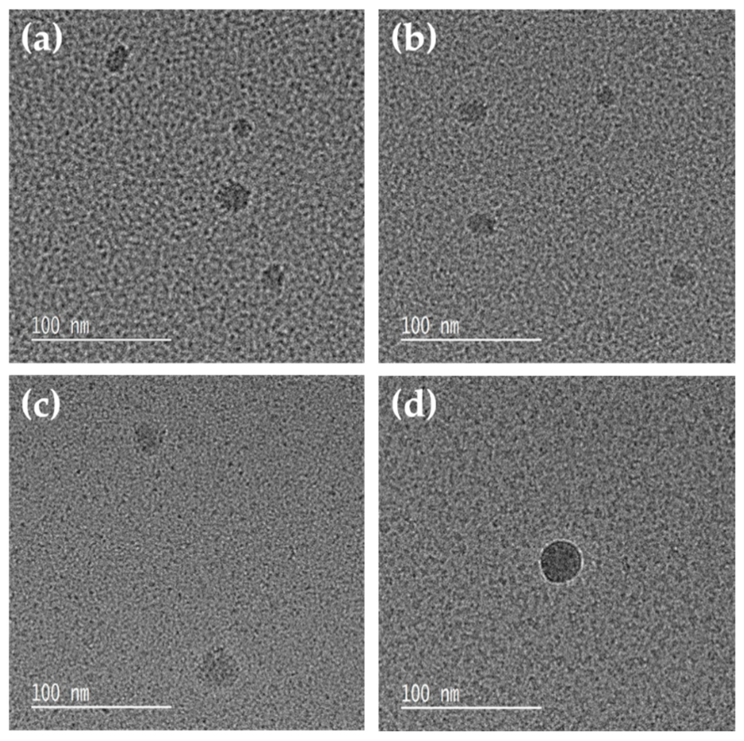
To check the size of nanoparticles, nanoparticles were captured for 10 s on a pure carbon membrane after delay times of 0, 2, 7, and 30 min using a quartz tube with a nozzle diameter of 10 mm. The TEM images of the captured nanoparticles are shown in
Figure 4. The size of the silicon oxide nanoparticles increased with increasing delay time. The average sizes of nanoparticles in
Figure 4a–d were 17, 70, 300, and 500 nm, respectively. Nanoparticles of 17 nm seem to be primary nanoparticles, which must have been formed initially by gas phase nucleation. Larger nanoparticles in
Figure 4b–d seem to grow by coalescence of primary nanoparticles.
The size was drastically increased with a delay time, which means that nanoparticles continue to grow with time inside the quartz tube of the CVD reactor. Especially after delay times of 7 and 30 min, nanoparticles grew to the very large size of 300 and 500 nm, respectively. The primary nanoparticles were always observed after delay times as shown in
Figure 4c,d. This means that the primary nanoparticles coexisted with large nanoparticles grown by coalescence of small or primary nanoparticles. This result indicates that the large nanoparticles in
Figure 4c,d had much larger residence time in the gas phase than the primary nanoparticles in
Figure 4a, implying that some nanoparticles circulated inside the quartz tube.
On the other hand, in the supersonic cluster beam deposition (SCBD) [
38,
39,
40], it is possible that the small primary nanoparticles aggregate forming a bigger nanostructure, while maintaining their individuality. This means that the small primary nanoparticles did not coalesce but only aggregated in contrast with our nanoparticles, which grow by coalescence of the small primary nanoparticles. One possible reason for the different behavior of nanoparticles to aggregate or coalesce would come from the temperature for coalescence to occur. In our experiment, the furnace temperature is as high as 1100 °C, which is high enough to make nanoparticles coalesce and lose their individuality. In contrast, in the SCBD process, the primary nanoparticles are expected to be cooled during supersonic expansion, which would be adiabatic. The aggregation of primary nanoparticles into a bigger nanostructure with their individuality maintained would be attributed to the low temperature.
Considering that the size of nanoparticles increased with increasing delay time, the deposition behavior in the initial stage can be quite different from that in the final stage. As a result, the film structure can be different between the initial and the final stages. Based on this, the structural change of films from the bottom to the top in
Figure 3e,f can be understood. In the initial stage of deposition, the size of nanoparticles is small and dense films would grow. As the deposition time increases, the size of nanoparticles would increase and the films would become a less dense and even porous structure with a rough surface as revealed in
Figure 3e,f.
The role of the nozzle is to accelerate the nanoparticles onto the substrate with the acceleration coming from the pressure difference between the quartz reactor and the deposition chamber which was evacuated by a rotary pump. Although the nozzle plays an important role in differential pumping and thereby accelerating nanoparticles, it seems to have a disadvantageous effect on the film deposition by circulating nanoparticles and increasing their size.
If the conical nozzle is really responsible for circulation of nanoparticles in the quartz tube, the circulation would be minimized by using the quartz tube without the nozzle. To check this possibility, we captured nanoparticles with delay times of 0, 2, 7, and 30 min using the quartz tube without the conical nozzle as shown in
Figure 1b. The result is shown in
Figure 5.
Figure 5 shows the nanoparticles captured for 10 s on a pure carbon membrane. The average sizes of nanoparticles in
Figure 5a–d are 20, 21, 22, and 27 nm, respectively. Although the particle size gradually increased with the delay time, there was no significant increase in size with delay time, compared to the case of a tube with a conical nozzle in
Figure 4. The result of
Figure 5 confirmed that the drastic increase in the size of the nanoparticles with delay time in
Figure 4 comes from the nozzle.
Comparing
Figure 4a and
Figure 5a, the size of primary particles (17 nm) in
Figure 4a is a little bit smaller than that (20 nm) in
Figure 5a. The reason would be that the residence time of the primary particles in
Figure 4a, which do not circulate but directly go into the deposition chamber, is shorter than that in
Figure 5a because the pressure difference between the quartz tube and the deposition chamber in
Figure 4a is much larger than that in
Figure 5a. Then, what would happen if the film is deposited using a quartz tube without a nozzle? Films much denser and more uniform than those of
Figure 3 are expected because the size of nanoparticles would not increase with the deposition time.
Figure 6 shows the top and cross section views of FESEM images of the films deposited on the Si substrate by the quartz tube without the nozzle as shown in
Figure 1b. The other deposition condition was the same as that of
Figure 3. As shown in
Figure 6a, unlike
Figure 3a, normally the surface is free of large particles. Also, the thickness of the film was 230 nm, which was uniform throughout the entire area. Although the film growth rate is lower than those of
Figure 3e,f, the area of deposition is much larger because there is no nozzle. Comparing
Figure 3f and
Figure 6b, we can say that if deposition is performed with only small nanoparticles, a dense film of uniform thickness can be obtained even at low temperatures.
As shown in
Figure 6, if a film was deposited with only small nanoparticles, a uniform film could be deposited. In this case, however, the length of the heating zone is 40 cm and the residence time of the precursor can be so short that it might not be sufficiently decomposed. If the carrier gas N
2 is preheated, it would be beneficial for the decomposition of the precursor. For this, we preheated N
2 by passing it through the heating zone through the stainless tube as shown in
Figure 1c. Except preheating and the flow rate of N
2, the other deposition condition was the same as that of
Figure 6.
Figure 7a,c shows, respectively, the FESEM images of the top and cross section views of thin films deposited using preheated N
2 at the flow rate of 5000 sccm while
Figure 7b,d shows, respectively, those of the top and cross section views of films deposited using preheated N
2 at the flow rate of 15,000 sccm.
Like
Figure 6a, large particles were hardly observed on the surface in
Figure 7a,b. In addition, the thickness of the film in
Figure 7c was 350 nm at the N
2 flow rate of 5000 sccm, which is about 50% thicker than 230 nm of the film in
Figure 6b. From
Figure 6b and
Figure 7c, it can be said that preheating of N
2 increased the decomposition rate of the precursor. At the N
2 flow rate of 15,000 sccm, the film was even thicker, being 530 nm as shown in
Figure 7d. It is not simple to understand the effect of the N
2 flow rate on the film growth rate. In the previous case of
Figure 2e,f, the increase in the flow rate of N
2 decreased the residence time of SiH
4 in the hot zone of the quartz tube and the precursor was not sufficiently decomposed, resulting in the decrease in the film thickness. This decomposition behavior might be changed when N
2 is preheated. A further possible reason that we can think of is that the higher flow rate of N
2 would increase the drag force and thereby increase the velocity of nanoparticles toward the substrate, resulting in the higher growth rate of the film.
The size distributions of captured nanoparticles as shown in
Figure 4 and
Figure 5 are shown in
Figure S1. As mentioned above, in the case of
Figure 4 with the conical nozzle, large particles of several hundred nanometers are formed as the delay increased to 7 min and 30 min. However, in the case of
Figure 5 without the nozzle, the size distributions of the nanoparticles become much narrower although it is bimodal. The overall size increases with increasing delay time.
The XRD peaks of the films deposited here did not show any peaks of the polycrystalline silicon but showed one peak of the single crystalline silicon, which would come from the substrate of the silicon wafer as shown in
Figure S2. This implies that the films would be amorphous. The composition analysis of the film surface by energy disperse spectroscopy (EDS) indicated a very high content of oxygen, indicating that silicon was oxidized and the films were silicon oxide as shown in
Table S1. The oxidation could not be prevented in our system, which was attributed to the relatively poor vacuum. If the oxidation can be prevented using a high vacuum system, the poly or nanocrystalline films might have been synthesized, which was revealed in the two-step growth using the hot wire CVD process [
21,
27,
28].
Dense films can be deposited by the two-step growth: gas phase nucleation of nanoparticles and growth of films by the building block of nanoparticles. In preparing the dense film with a smooth surface, the most significant requirement is the small size of the nanoparticles. According to the previous study [
23,
24], nanoparticles in this study are expected to be electrically charged and the presence of charge plays an important role in the growth of dense films.
Under typical conditions of film deposition by chemical vapor deposition, it was shown that charged nanoparticles are generated in the gas phase and contribute to film deposition [
11]. In order to examine the effect of charge carried by nanoparticles on the deposition behavior, Youn et al. [
24] compared the deposition behavior between electrically floating and grounded silicon substrates. They observed that single crystalline silicon nanowires grew on the floating substrate whereas nanoparticles were deposited on the grounded substrate. When they increased the flow rate of carrier N
2 gas from 500 sccm to 1000 sccm, they observed that a dense film was deposited on the floating substrate whereas a porous film was deposited on the grounded substrate.
However, this study focused on the possibility that the precursor can be decomposed at high temperatures and deposited at low temperatures by the two-step growth mechanism. If this concept is applied, films can be deposited at low temperatures, using the low-cost precursor, which can be decomposed only at high temperatures.


