Glancing Angle Deposition and Growth Mechanism of Inclined AlN Nanostructures Using Reactive Magnetron Sputtering

 ,
,  and
and 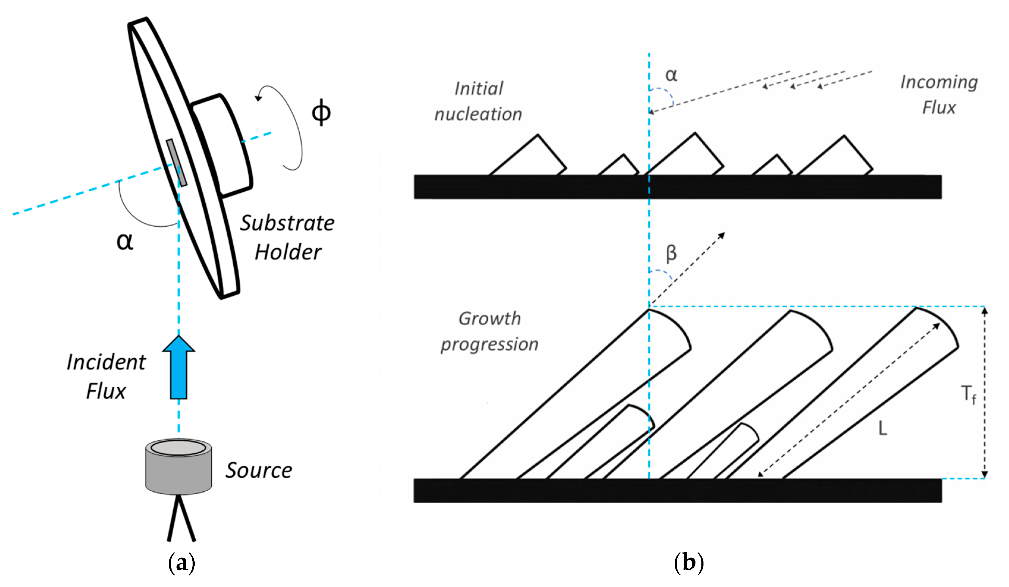
Abstract
:1. Introduction
2. Materials and Methods
3. Results
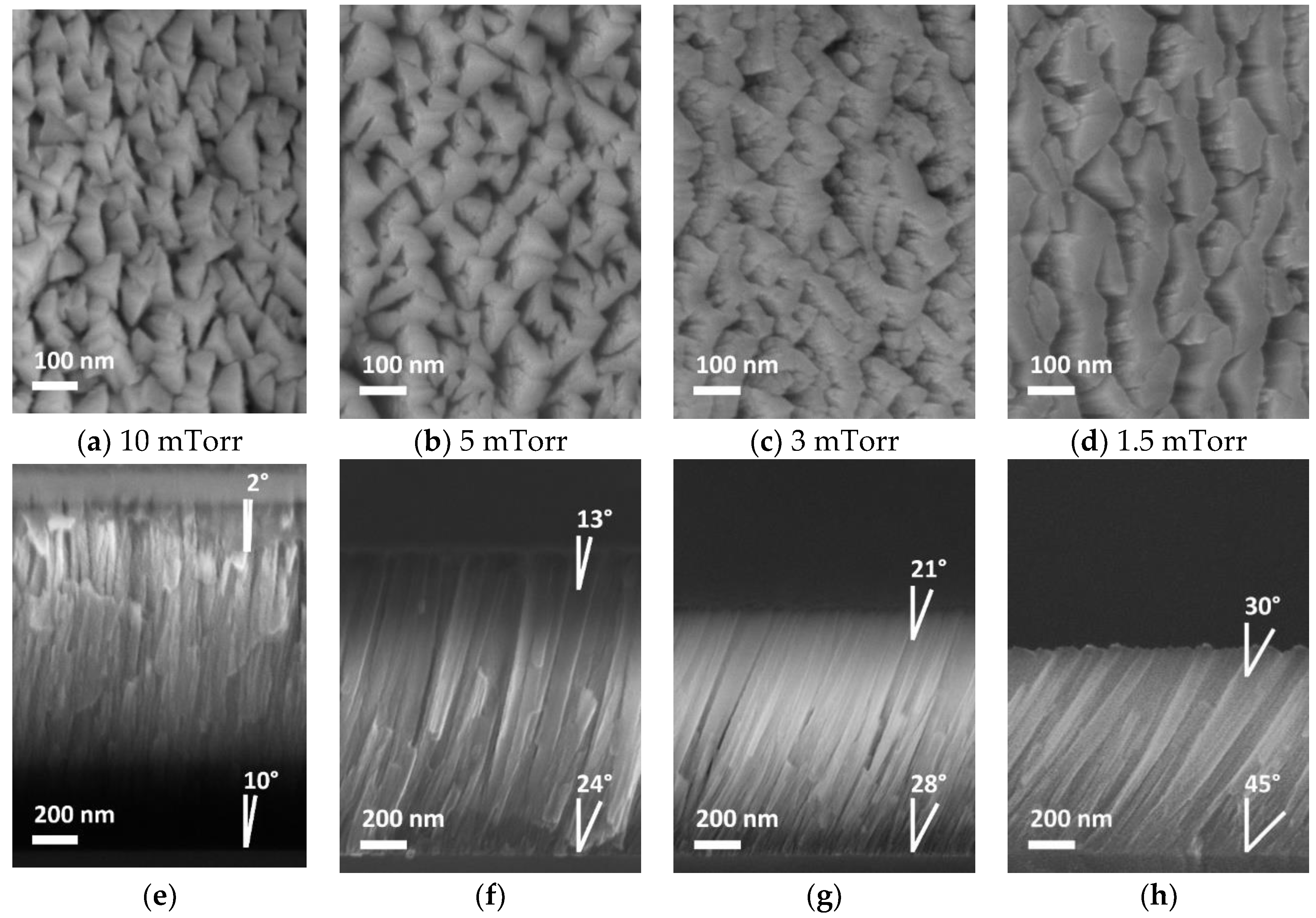
3.1. Morphological Characteristics of Glancing Angle Deposition (GLAD) AlN Films
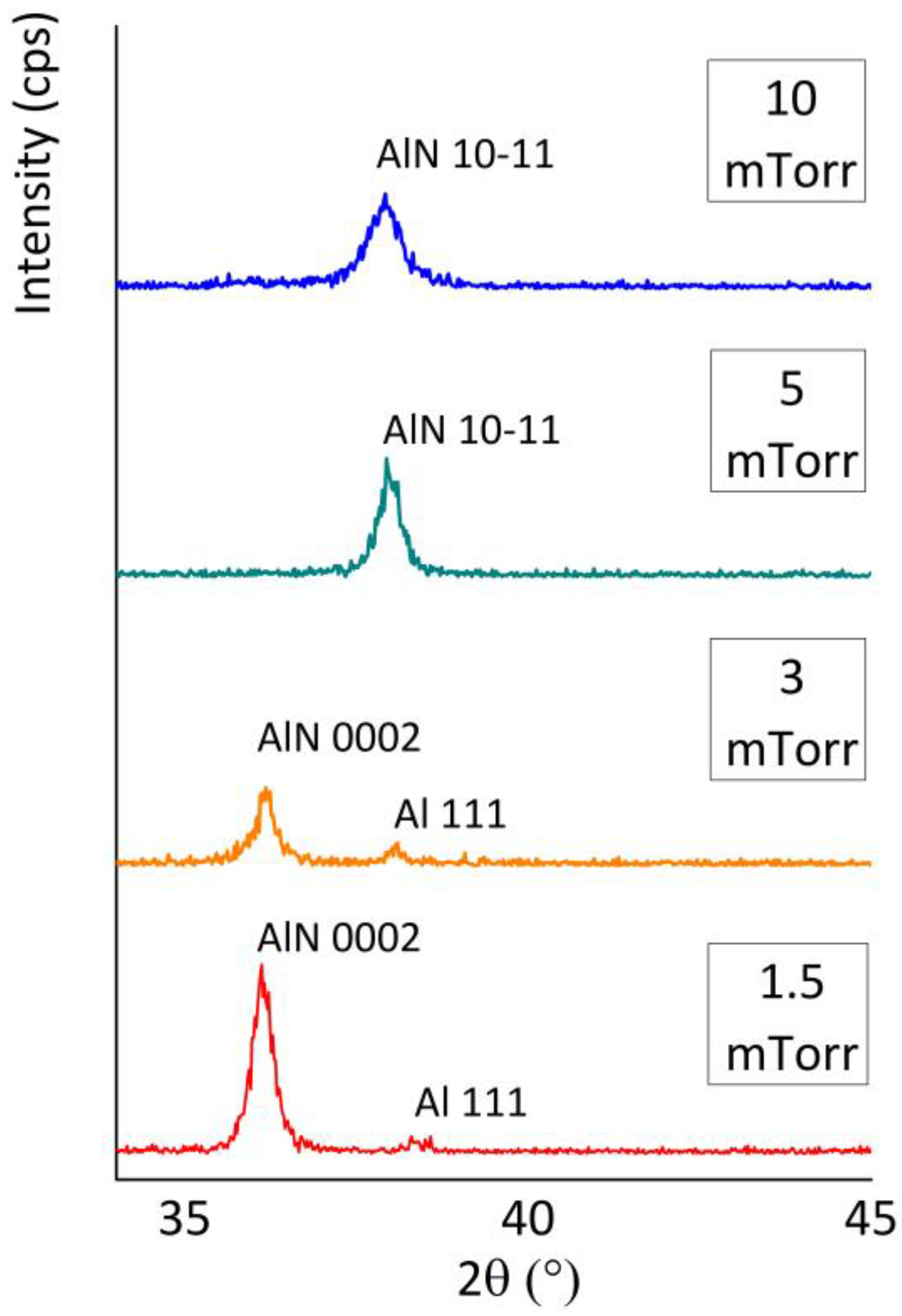
3.2. Crystallographic Characteristics
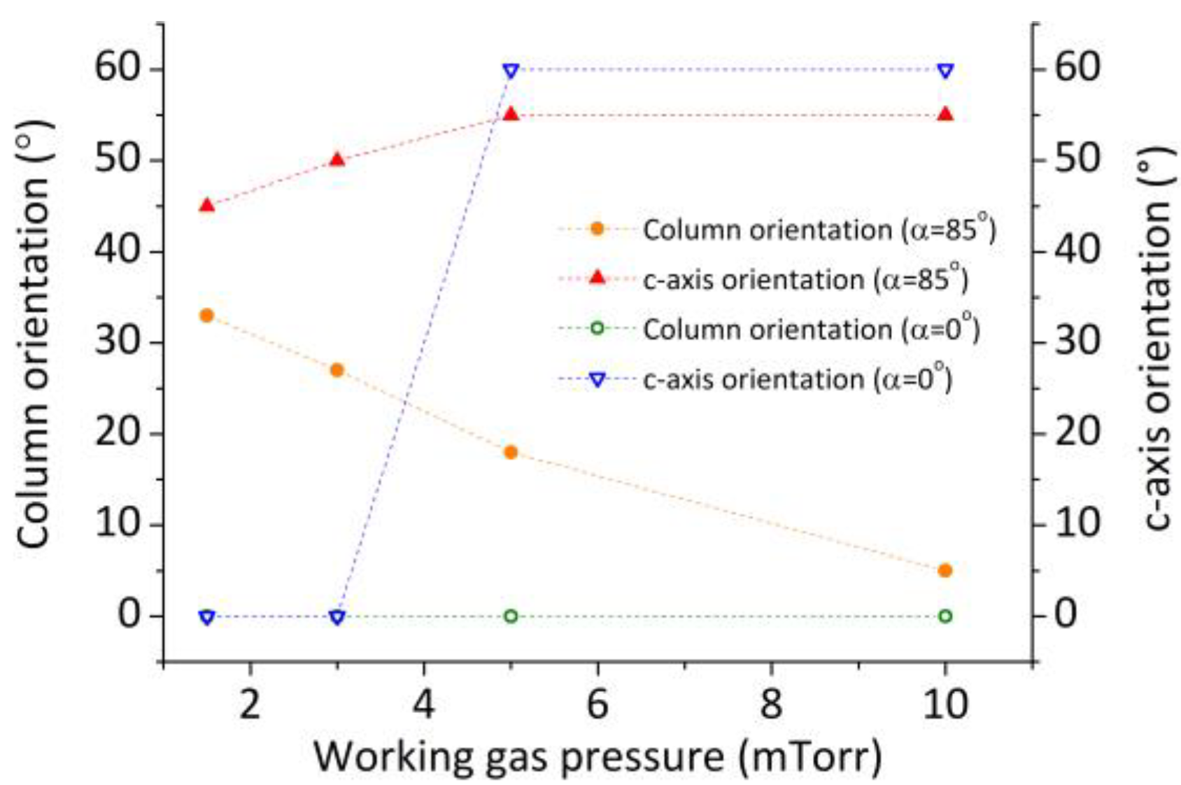
3.2.1. GLAD: α = 85°
3.2.2. Normal Deposition: α = 0°
3.2.3. Short-Time Growth for Both α = 85° and 0°
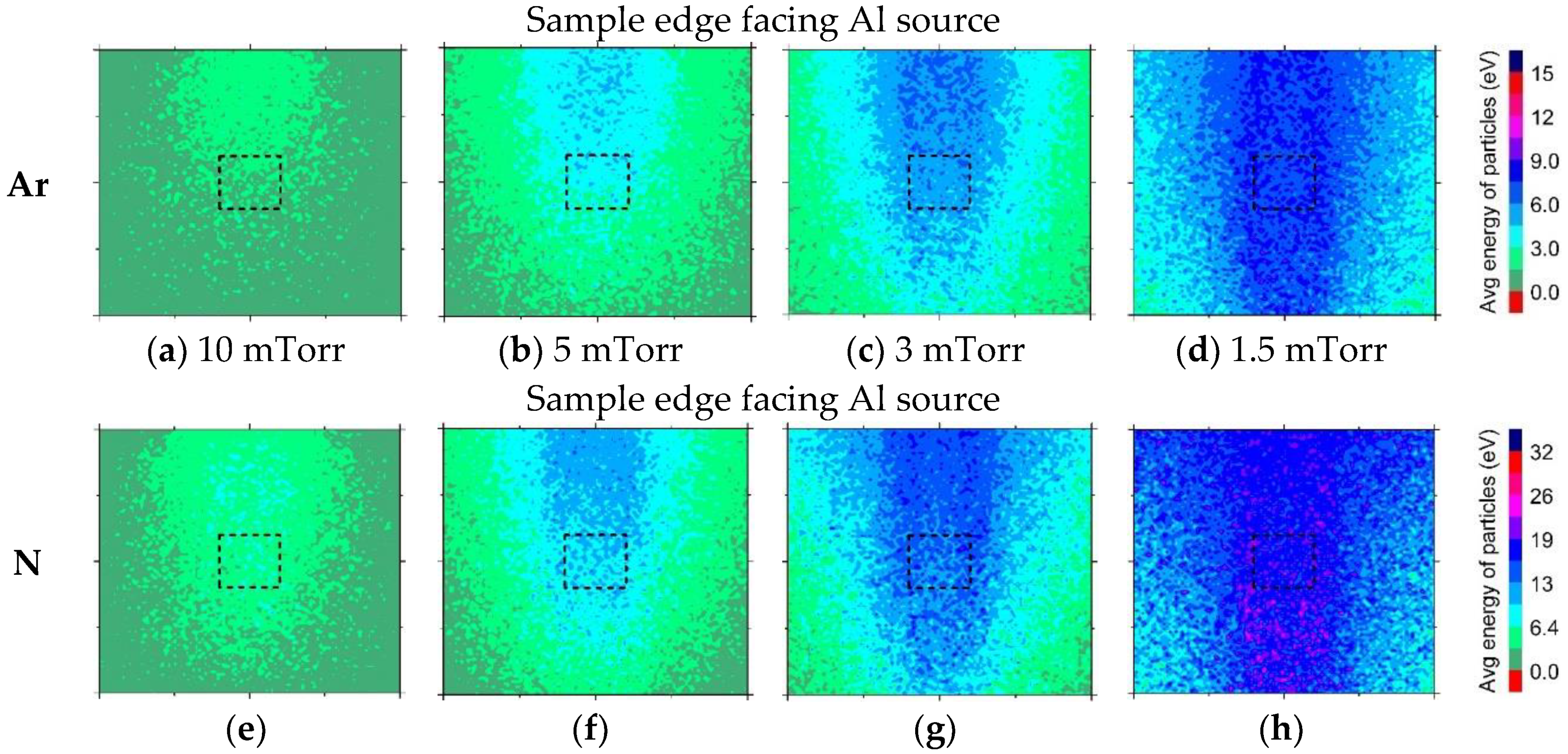
3.3. Metal Flux Simulations
4. Discussion
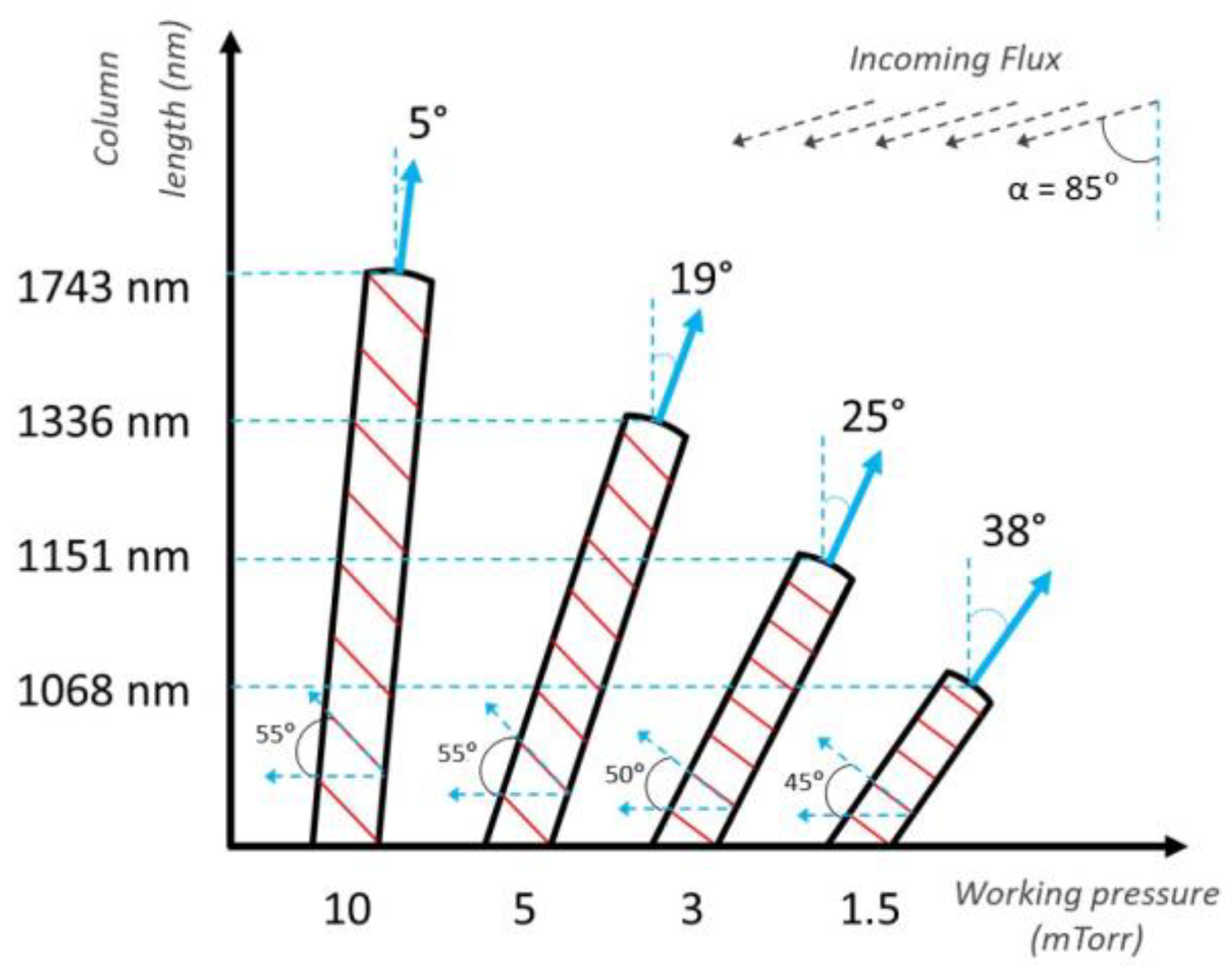
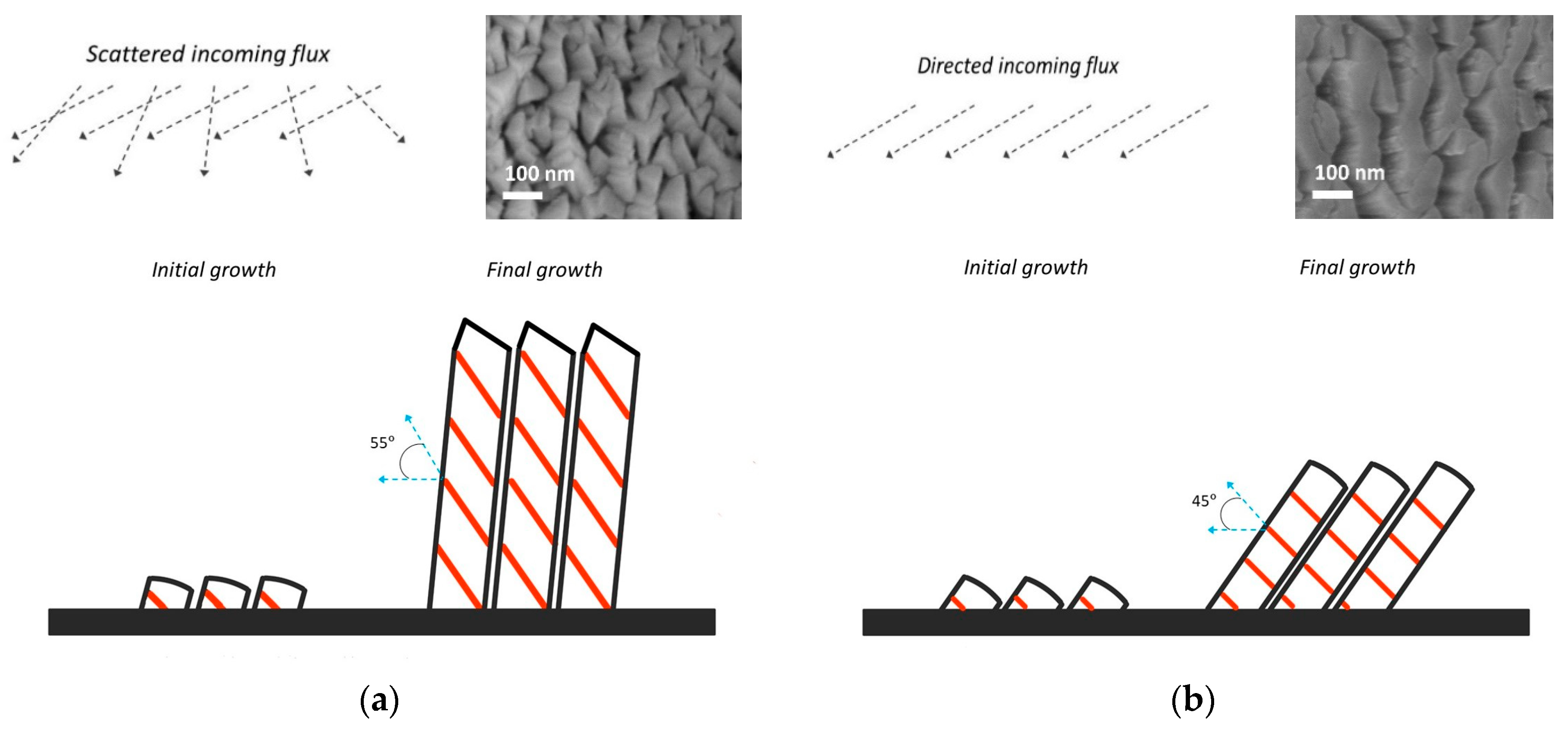
4.1. GLAD Configuration
4.2. Variation in Biaxial Texture in GLAD Columnar Films
4.3. Evolution of AlN Crystal Plane with Working Pressure in Normal Deposition Configuration
5. Conclusions
Author Contributions
Funding
Conflicts of Interest
References
- Hochbaum, A.I.; Yang, P. Semiconductor nanowires for energy conversion. Chem. Rev. 2010, 110, 527–546. [Google Scholar] [CrossRef]
- Szczech, J.R.; Higgins, J.M.; Jin, S. Enhancement of the thermoelectric properties in nanoscale and nanostructured materials. J. Mater. Chem. 2011, 21, 4037–4055. [Google Scholar] [CrossRef]
- Bierman, M.J.; Jin, S. Potential applications of hierarchical branching nanowires in solar energy conversion. Energy Environ. Sci. 2009, 2, 1050. [Google Scholar] [CrossRef]
- Pişkin, F.; Bliem, R.; Yildiz, B. Effect of crystal orientation on the segregation of aliovalent dopants at the surface of La0.6Sr0.4CoO3. J. Mater. Chem. A 2018, 6, 14136–14145. [Google Scholar] [CrossRef] [Green Version]
- Wang, R.; Tong, Y.; Manzi, A.; Wang, K.; Fu, Z.; Kentzinger, E.; Feldmann, J.; Urban, A.S.; Müller-Buschbaum, P.; Frielinghaus, H. Preferential orientation of crystals induced by incorporation of organic ligands in mixed-dimensional hybrid perovskite films. Adv. Opt. Mater. 2018, 6, 1701311. [Google Scholar] [CrossRef]
- Hu, Y.; Zhu, J.; Zhang, C.; Yang, W.; Fu, L.; Li, D.; Zhou, L. Understanding the preferred crystal orientation of sputtered silver in Ar/N2 atmosphere: A microstructure investigation. Adv. Mater. Sci. Eng. 2019, 1–8. [Google Scholar] [CrossRef] [Green Version]
- Yang, B.; Wang, C.; Yuan, Z.; Chen, S.; He, Y.; Song, H.; Ding, R.; Zhao, Y.; Tang, J. Hydrazine solution processed CuSbSe2: Temperature dependent phase and crystal orientation evolution. Sol. Energy Mater. Sol. Cells 2017, 168, 112–118. [Google Scholar] [CrossRef]
- Ruys, A. Alumina as an electrical insulator. In Alumina Ceramics; Elsevier: Amsterdam, The Netherlands, 2019; pp. 413–445. [Google Scholar]
- Mylvaganam, K.; Chen, Y.; Liu, W.; Liu, M.; Zhang, L. Hard thin films: Applications and challenges. In Anti-Abrasive Nanocoatings: Current and Future Applications; Elsevier Inc.: Amsterdam, The Netherlands, 2014; pp. 544–567. ISBN 9780857092175. [Google Scholar]
- Petti, C.J.; Hilali, M.M.; Prabhu, G. Thin Films in Photovoltaics. In Handbook of Thin Film Deposition: Techniques, Processes, and Technologies, 3rd ed.; Elsevier Inc.: Amsterdam, The Netherlands, 2012; pp. 313–359. ISBN 9781437778748. [Google Scholar]
- Iqbal, A.; Walker, G.; Iacopi, A.; Mohd-Yasin, F. Controlled sputtering of AlN (002) and (101) crystal orientations on epitaxial 3C-SiC-on-Si (100) substrate. J. Cryst. Growth 2016, 440, 76–80. [Google Scholar] [CrossRef]
- Greene, J.E. Tracing the 5000-year recorded history of inorganic thin films from ∼3000 BC to the early 1900s AD. Appl. Phys. Rev. 2014, 1, 41302. [Google Scholar] [CrossRef] [Green Version]
- Robbie, K.; Brett, M.J.; Lakhtakia, A. Chiral sculptured thin films. Nature 1996, 384, 616. [Google Scholar] [CrossRef]
- Jen, Y.-J.; Lin, C.-F. Anisotropic optical thin films finely sculptured by substrate sweep technology. Opt. Express 2008, 16, 5372–5377. [Google Scholar] [CrossRef]
- Pessoa, R.S.; Fraga, M.A. Biomedical applications of ultrathin atomic layer deposited metal oxide films on polymeric materials. Front. Nanosci. 2019, 14, 291–307. [Google Scholar]
- Lein, H.L. Coatings and surfaces with hydrophobic and anti-icing properties. Front. Nanosci. 2019, 14, 257–269. [Google Scholar]
- Miranti, R.; Parisi, J. Spectroscopic and electrical properties of hybrid thin films for solar cell applications. Front. Nanosci. 2019, 14, 271–290. [Google Scholar]
- Hawkeye, M.M.; Brett, M.J. Glancing angle deposition: Fabrication, properties, and applications of micro- and nanostructured thin films. J. Vac. Sci. Technol. A Vac. Surf. Films 2007, 25, 1317–1335. [Google Scholar] [CrossRef]
- Barranco, A.; Borras, A.; Gonzalez-Elipe, A.R.; Palmero, A. Perspectives on oblique angle deposition of thin films: From fundamentals to devices. Prog. Mater. Sci. 2016, 76, 59–153. [Google Scholar] [CrossRef] [Green Version]
- Zhou, C.M.; Gall, D. Development of two-level porosity during glancing angle deposition. J. Appl. Phys. 2008, 103, 14307. [Google Scholar] [CrossRef]
- Kundt, A. Ueber doppelbrechung des lichtes in metallschichten, welche durch zerstäuben einer kathode hergestellt sind. Ann. Phys. Chem. 1886, 263, 59–71. [Google Scholar] [CrossRef] [Green Version]
- Salinger, H.; Beutler, E. Der König in Thule und die dichtungen von der lorelay. Books Abroad 1950, 24, 64. [Google Scholar] [CrossRef]
- Liedtke, S.; Grüner, C.; Lotnyk, A.; Rauschenbach, B. Glancing angle deposition of sculptured thin metal films at room temperature. Nanotechnology 2017, 28, 385604. [Google Scholar] [CrossRef] [Green Version]
- Besnard, A.; Martin, N.; Millot, C.; Gavoille, J.; Salut, R. Effect of sputtering pressure on some properties of chromium thin films obliquely deposited. IOP Conf. Ser. Mater. Sci. Eng. 2010, 12, 12015. [Google Scholar] [CrossRef]
- Messier, R.F.; Sunal, P.D.; Venugopal, V.C. Evolution of sculptured thin films. Eng. Nanostruct. Films Mater. 1999, 3790, 133–141. [Google Scholar]
- Suzuki, M. Practical applications of thin films nanostructured by shadowing growth. J. Nanophotonics 2013, 7, 73598. [Google Scholar] [CrossRef]
- Kesapragada, S.V.; Sotherland, P.R.; Gall, D. Ta nanotubes grown by glancing angle deposition. J. Vac. Sci. Technol. B Microelectron. Nanometer Struct. 2008, 26, 678. [Google Scholar] [CrossRef]
- Zhou, C.M.; Gall, D. The structure of Ta nanopillars grown by glancing angle deposition. Thin Solid Films 2006, 515, 1223–1227. [Google Scholar] [CrossRef]
- Charles, C.; Martin, N.; Devel, M. Optical properties of nanostructured WO3 thin films by glancing angle deposition: Comparison between experiment and simulation. Surf. Coat. Technol. 2015, 276, 136–140. [Google Scholar] [CrossRef]
- Xu, X.; Arab Pour Yazdi, M.; Sanchez, J.-B.; Billard, A.; Berger, F.; Martin, N. Exploiting the dodecane and ozone sensing capabilities of nanostructured tungsten oxide films. Sens. Actuators B Chem. 2018, 266, 773–783. [Google Scholar] [CrossRef]
- Lakhtakia, A. Sculptured thin films: Accomplishments and emerging uses. Mater. Sci. Eng. C 2002, 19, 427–434. [Google Scholar] [CrossRef] [Green Version]
- Lintymer, J.; Martin, N.; Chappé, J.-M.; Delobelle, P.; Takadoum, J. Nanoindentation of chromium zigzag thin films sputter deposited. Surf. Coat. Technol. 2005, 200, 269–272. [Google Scholar] [CrossRef]
- Singh, J.P.; Tang, F.; Karabacak, T.; Lu, T.-M.; Wang, G.-C. Enhanced cold field emission from 〈100〉 oriented β–W nanoemitters. J. Vac. Sci. Technol. B Microelectron. Nanometer Struct. 2004, 22, 1048. [Google Scholar] [CrossRef]
- Singh, A.; Sharma, A.; Tomar, M.; Gupta, V. Tunable nanostructured columnar growth of SnO2 for efficient detection of CO gas. Nanotechnology 2018, 29, 65502. [Google Scholar] [CrossRef]
- Xi, J.-Q.; Schubert, M.F.; Kim, J.K.; Schubert, E.F.; Chen, M.; Lin, S.-Y.; Liu, W.; Smart, J.A. Optical thin-film materials with low refractive index for broadband elimination of Fresnel reflection. Nat. Photonics 2007, 1, 176–179. [Google Scholar] [CrossRef]
- Parra-Barranco, J.; Oliva-Ramirez, M.; Gonzalez-Garcia, L.; Alcaire, M.; Macias-Montero, M.; Borras, A.; Frutos, F.; Gonzalez-Elipe, A.R.; Barranco, A. Bending induced self-organized switchable gratings on polymeric substrates. ACS Appl. Mater. Interfaces 2014, 6, 11924–11931. [Google Scholar] [CrossRef]
- Chi, P.-W.; Su, C.-W.; Wei, D.-H. Control of hydrophobic surface and wetting states in ultra-flat ZnO films by GLAD method. Appl. Surf. Sci. 2017, 404, 380–387. [Google Scholar] [CrossRef]
- Allenstein, U.; Wisotzki, E.I.; Gräfe, C.; Clement, J.H.; Liu, Y.; Schroers, J.; Mayr, S.G. Binary Fe-Pd submicron structures fabricated through glancing angle deposition (GLAD) for bioapplications. Mater. Des. 2017, 131, 366–374. [Google Scholar] [CrossRef]
- Petrov, I.; Barna, P.B.; Hultman, L.; Greene, J.E. Microstructural evolution during film growth. J. Vac. Sci. Technol. A Vac. Surf. Films 2003, 21, S117–S128. [Google Scholar] [CrossRef]
- Hsiao, C.L.; Palisaitis, J.; Persson, P.O.Å.; Junaid, M.; Serban, E.A.; Sandström, P.; Hultman, L.; Birch, J. Nucleation and core-shell formation mechanism of self-induced InxAl1–xN core-shell nanorods grown on sapphire substrates by magnetron sputter epitaxy. Vacuum 2016, 131, 39–43. [Google Scholar] [CrossRef] [Green Version]
- Serban, E.A.; Palisaitis, J.; Yeh, C.C.; Hsu, H.C.; Tsai, Y.L.; Kuo, H.C.; Junaid, M.; Hultman, L.; Persson, P.O.Å.; Birch, J.; et al. Selective-area growth of single-crystal wurtzite GaN nanorods on SiOx/Si(001) substrates by reactive magnetron sputter epitaxy exhibiting single-mode lasing. Sci. Rep. 2017, 7, 1–11. [Google Scholar]
- Niewehuizen, J.M.; Haanstra, H.B. Microfractography of thin films. Philips Tech. Rev. 1966, 27, 87–91. [Google Scholar]
- Tait, R.N.; Smy, T.; Brett, M.J. Modelling and characterization of columnar growth in evaporated films. Thin Solid Films 1993, 226, 196–201. [Google Scholar] [CrossRef]
- Meakin, P. Ballistic deposition onto inclined surfaces. Phys. Rev. A 1988, 38, 994–1004. [Google Scholar] [CrossRef]
- Lichter, S.; Chen, J. Model for columnar microstructure of thin solid films. Phys. Rev. Lett. 1986, 56, 1396–1399. [Google Scholar] [CrossRef]
- Tanto, B.; Ten Eyck, G.; Lu, T.-M.M. A model for column angle evolution during oblique angle deposition. J. Appl. Phys. 2010, 108, 2008–2011. [Google Scholar] [CrossRef]
- Grüner, C.; Liedtke, S.; Bauer, J.; Mayr, S.G.; Rauschenbach, B. Morphology of thin films formed by oblique physical vapor deposition. ACS Appl. Nano Mater. 2018, 1, 1370–1376. [Google Scholar] [CrossRef]
- Shetty, A.R.; Karimi, A. Texture mechanisms and microstructure of biaxial thin films grown by oblique angle deposition. Phys. Status Solidi Basic Res. 2012, 249, 1531–1540. [Google Scholar] [CrossRef]
- Wu, Q. Circular polarization filters made of chiral sculptured thin films: Experimental and simulation results. Opt. Eng. 2000, 39, 1863. [Google Scholar] [CrossRef]
- Lakhtakia, A. Experimental realization of sculptured-thin-film polarization-discriminatory light-handedness inverters. Opt. Eng. 2000, 39, 2831–2834. [Google Scholar] [CrossRef]
- Hodgkinson, I.J.; Wu, Q.H.; Lakhtakia, A.; McCall, M.W. Spectral-hole filter fabricated using sculptured thin-film technology. Opt. Commun. 2000, 177, 79–84. [Google Scholar] [CrossRef]
- García-Méndez, M.; Morales-Rodríguez, S.; Machorro, R.; De La Cruz, W. Characterization of ALN thin films deposited by DC reactive magnetron sputtering. Rev. Mex. Fis. 2008, 54, 271–278. [Google Scholar]
- Zhang, X.-H.H.; Shao, R.-W.W.; Jin, L.; Wang, J.-Y.Y.; Zheng, K.; Zhao, C.-L.L.; Han, J.-C.C.; Chen, B.; Sekiguchi, T.; Zhang, Z.; et al. Helical growth of aluminum nitride: New insights into its growth habit from nanostructures to single crystals. Sci. Rep. 2015, 5, 1–12. [Google Scholar] [CrossRef] [Green Version]
- Wu, Q.; Hu, Z.; Wang, X.; Lu, Y.; Chen, X.; Xu, H.; Chen, Y. Synthesis and characterization of faceted hexagonal aluminum nitride nanotubes. J. Am. Chem. Soc. 2003, 125, 10176–10177. [Google Scholar] [CrossRef]
- Wu, Q.; Hu, Z.; Wang, X.; Chen, Y.; Lu, Y.; Qiang, W.; Zheng, H.; Xizhang, W.; Chen, Y.; Lu, Y.; et al. Synthesis and optical characterization of aluminum nitride nanobelts. J. Phys. Chem. B 2003, 107, 9726–9729. [Google Scholar] [CrossRef]
- Wu, Q.; Hu, Z.; Wang, X.; Lu, Y.; Huo, K.; Deng, S.; Xu, N.; Shen, B.; Zhang, R.; Chen, Y. Extended vapor–liquid–solid growth and field emission properties of aluminium nitride nanowires. J. Mater. Chem. 2003, 13, 2024–2027. [Google Scholar] [CrossRef]
- Mahieu, S.; Ghekiere, P.; Depla, D.; De Gryse, R. Biaxial alignment in sputter deposited thin films. Thin Solid Films 2006, 515, 1229–1249. [Google Scholar] [CrossRef] [Green Version]
- Deng, R.; Muralt, P.; Gall, D. Biaxial texture development in aluminum nitride layers during off-axis sputter deposition. J. Vac. Sci. Technol. A Vac. Surf. Films 2012, 30, 51501. [Google Scholar] [CrossRef]
- Article, R.; Bogaerts, A.; Bultinck, E.; Kolev, I. The metal flux from a rotating cylindrical magnetron. J. Phys. D Appl. Phys. 2008, 41, 205307. [Google Scholar]
- Hsiao, C.-L.; Magnusson, R.; Palisaitis, J.; Sandström, P.; Persson, P.O.Å.; Valyukh, S.; Hultman, L.; Järrendahl, K.; Birch, J. Curved-lattice epitaxial growth of InxAl1–xN nanospirals with tailored chirality. Nano Lett. 2014, 15, 294–300. [Google Scholar] [CrossRef]
- Kuo, Y.-H.H.; Magnusson, R.; Serban, E.A.; Sandström, P.; Hultman, L.; Järrendahl, K.; Birch, J.; Hsiao, C.-L.L. Influence of InALN nanospiral structures on the behavior of reflected light polarization. Nanomaterials 2018, 8, 157. [Google Scholar] [CrossRef] [Green Version]
- James Ziegler—SRIM & TRIM. Available online: http://www.srim.org/index.htm#HOMETOP (accessed on 14 June 2020).
- Alvarez, R.; Garcia-Martin, J.M.; Garcia-Valenzuela, A.; Macias-Montero, M.; Ferrer, F.J.; Santiso, J.; Rico, V.; Cotrino, J.; Gonzalez-Elipe, A.R.; Palmero, A. Nanostructured Ti thin films by magnetron sputtering at oblique angles. J. Phys. D Appl. Phys. 2015, 49, 45303. [Google Scholar] [CrossRef] [Green Version]
- Cheng, H.; Sun, Y.; Hing, P. The influence of deposition conditions on structure and morphology of aluminum nitride films deposited by radio frequency reactive sputtering. Thin Solid Films 2003, 434, 112–120. [Google Scholar] [CrossRef]
- Zhou, X.W.; Wadley, H.N.G. Hyperthermal vapor deposition of copper: Athermal and biased diffusion effects. Surf. Sci. 1999, 431, 42–57. [Google Scholar] [CrossRef]
- Jindal, V.; Shahedipour-Sandvik, F. Density functional theoretical study of surface structure and adatom kinetics for wurtzite AlN. J. Appl. Phys. 2009, 105, 84902. [Google Scholar] [CrossRef]
- Kajikawa, Y.; Noda, S.; Komiyama, H. Comprehensive perspective on the mechanism of preferred orientation in reactive-sputter-deposited nitrides. J. Vac. Sci. Technol. A Vac. Surf. Films 2003, 21, 1943–1954. [Google Scholar] [CrossRef]
- Gall, D.; Petrov, I.; Hellgren, N.; Hultman, L.; Sundgren, J.E.; Greene, J.E. Growth of poly- and single-crystal ScN on MgO(001): Role of low-energy N2+ irradiation in determining texture, microstructure evolution, and mechanical properties. J. Appl. Phys. 1998, 84, 6034–6041. [Google Scholar] [CrossRef] [Green Version]
- Gall, D.; Kodambaka, S.; Wall, M.A.; Petrov, I.; Greene, J.E. Pathways of atomistic processes on TiN(001) and (111) surfaces during film growth: Anab initiostudy. J. Appl. Phys. 2003, 93, 9086–9094. [Google Scholar] [CrossRef] [Green Version]
- Xu, X.H.; Wu, H.S.; Zhang, C.J.; Jin, Z.H. Morphological properties of AlN piezoelectric thin films deposited by DC reactive magnetron sputtering. Thin Solid Films 2001, 388, 62–67. [Google Scholar] [CrossRef]
- Cheng, H.; Sun, Y.; Hing, P. Microstructure evolution of AIN films deposited under various pressures by RF reactive sputtering. Surf. Coat. Technol. 2003, 166, 231–236. [Google Scholar] [CrossRef]
- Mahieu, S.; Ghekiere, P.; De Winter, G.; Heirwegh, S.; Depla, D.; De Gryse, R.; Lebedev, O.I.; Van Tendeloo, G. Mechanism of preferential orientation in sputter deposited titanium nitride and yttria-stabilized zirconia layers. J. Cryst. Growth 2005, 279, 100–109. [Google Scholar] [CrossRef]
- Iqbal, A.; Mohd-Yasin, F. Reactive sputtering of aluminum nitride (002) thin films for piezoelectric applications: A review. Sensors 2018, 18, 1797. [Google Scholar] [CrossRef] [Green Version]
- Taurino, A.; Signore, M.A.; Catalano, M.; Kim, M.J. (101) and (002) oriented AlN thin films deposited by sputtering. Mater. Lett. 2017, 200, 18–20. [Google Scholar] [CrossRef]
- Kar, J.P.; Bose, G.; Tuli, S. A study on the interface and bulk charge density of AlN films with sputtering pressure. Vacuum 2006, 81, 494–498. [Google Scholar] [CrossRef]
- Cheng, H.; Sun, Y.; Zhang, J.X.; Zhang, Y.B.; Yuan, S.; Hing, P. AlN films deposited under various nitrogen concentrations by RF reactive sputtering. J. Cryst. Growth 2003, 254, 46–54. [Google Scholar] [CrossRef]
- Cheng, H. Preparation of [002] oriented AlN thin films by mid frequency reactive sputtering technique. Thin Solid Films 2003, 425, 85–89. [Google Scholar] [CrossRef]
- Singh, A.V.; Chandra, S.; Bose, G. Deposition and characterization of c-axis oriented aluminum nitride films by radio frequency magnetron sputtering without external substrate heating. Thin Solid Films 2011, 519, 5846–5853. [Google Scholar] [CrossRef]


© 2020 by the authors. Licensee MDPI, Basel, Switzerland. This article is an open access article distributed under the terms and conditions of the Creative Commons Attribution (CC BY) license (http://creativecommons.org/licenses/by/4.0/).
Share and Cite
Bairagi, S.; Järrendahl, K.; Eriksson, F.; Hultman, L.; Birch, J.; Hsiao, C.-L. Glancing Angle Deposition and Growth Mechanism of Inclined AlN Nanostructures Using Reactive Magnetron Sputtering. Coatings 2020, 10, 768. https://doi.org/10.3390/coatings10080768
Bairagi S, Järrendahl K, Eriksson F, Hultman L, Birch J, Hsiao C-L. Glancing Angle Deposition and Growth Mechanism of Inclined AlN Nanostructures Using Reactive Magnetron Sputtering. Coatings. 2020; 10(8):768. https://doi.org/10.3390/coatings10080768
Chicago/Turabian StyleBairagi, Samiran, Kenneth Järrendahl, Fredrik Eriksson, Lars Hultman, Jens Birch, and Ching-Lien Hsiao. 2020. "Glancing Angle Deposition and Growth Mechanism of Inclined AlN Nanostructures Using Reactive Magnetron Sputtering" Coatings 10, no. 8: 768. https://doi.org/10.3390/coatings10080768