Article

Effects of Nitrogen Flow Ratio on Structures, Bonding Characteristics, and Mechanical Properties of ZrNx Films

1
Department of Optoelectronics and Materials Technology, National Taiwan Ocean University, Keelung 20224, Taiwan
2
Center of Excellence for Ocean Engineering, National Taiwan Ocean University, Keelung 20224, Taiwan
*
Author to whom correspondence should be addressed.
Coatings 2020, 10(5), 476; https://doi.org/10.3390/coatings10050476
Submission received: 11 April 2020 / Revised: 1 May 2020 / Accepted: 12 May 2020 / Published: 14 May 2020
(This article belongs to the Special Issue Physical Vapor Deposition)

Abstract

:
ZrNx (x = 0.67–1.38) films were fabricated through direct current magnetron sputtering by a varying nitrogen flow ratio [N2/(Ar + N2)] ranging from 0.4 to 1.0. The structural variation, bonding characteristics, and mechanical properties of the ZrNx films were investigated. The results indicated that the structure of the films prepared using a nitrogen flow ratio of 0.4 exhibited a crystalline cubic ZrN phase. The phase gradually changed to a mixture of crystalline ZrN and orthorhombic Zr3N4 followed by a Zr3N4 dominant phase as the N2 flow ratio increased up to >0.5 and >0.85, respectively. The bonding characteristics of the ZrNx films comprising Zr–N bonds of ZrN and Zr3N4 compounds were examined by X-ray photoelectron spectroscopy and were well correlated with the structural variation. With the formation of orthorhombic Zr3N4, the nanoindentation hardness and Young’s modulus levels of the ZrNx (x = 0.92–1.38) films exhibited insignificant variations ranging from 18.3 to 19.0 GPa and from 210 to 234 GPa, respectively.

1. Introduction

Multifunctional ZrN films have been extensively investigated due to their characteristics including golden yellow appearance [1,2,3], high hardness [3,4,5,6], corrosion resistance [7,8,9], and wear resistance [10]. The nitrogen flow rate in reactive sputtering affects the structure and composition of fabricated MeNx (Me = Ti, Zr, Hf) films [11,12,13], which varied the characteristics of these films. The B1 structure is a familiar structure for transition metal nitrides, in which N occupies the interstitial sites of close-packed metal atoms. Moreover, a wide composition range, with point defects in the B1 structure, was obtained for transition metal nitrides [14]. By contrast, N-rich compounds such as Ti3N4, Zr3N4, and Hf3N4 have been reported [15]. Zr3N4 crystallizes in an orthorhombic (o-Zr3N4) [16,17,18] or cubic (c-Zr3N4) [19,20,21,22,23] phase. o-Zr3N4 was reported as a transparent insulator [16,24], whereas c-Zr3N4 with a cubic Th3P4-type structure was suggested as an alternating hard material [19,23]. Mattesini et al., [23] reported the calculated hardness level of c-Zr3N4 to be 17.5–19.7 GPa. Chhowalla and Unalan [25] announced that the filtered cathodic arc fabricated c-Zr3N4 films stabilized by a high residual stress and showed a high hardness of 36 GPa, compared to 27 GPa for the low-stressed o-Zr3N4 films. Zr3N4 contained films fabricated through sputtering technologies that were also reported either in the o-Zr3N4 or the c-Zr3N4 forms [12,16,18,26,27]. Previous studies [12,16,28] have reported that interstitial N is incorporated into the ZrN structure to form a Zr3N4 phase as the nitrogen flow ratio was higher than the critical level to form stoichiometric ZrN. Takeyama et al., [18] reported that a bilayered ZrN/o-Zr3N4 barrier was thermally stable undergoing the annealing at 500 °C for 60 min, but the o-Zr3N4 barrier was metastable in the Zr–N system. Kroll [15] proposed that c-Zr3N4 is obtained in a high-pressure state. Alternatively, Meng et al., [27] reported the phase transformation from ZrN to c-Zr3N4 under high-compressive stress by increasing the substrate bias voltage in direct current magnetron sputtering (DCMS). In a previous study [29], HfNx films with stoichiometric variable x in the range of 0.81–2.07 were deposited through DCMS using nitrogen flow ratios of 0.1 to 1.0. The structure varied from a δ-HfN phase to a near-amorphous structure as the stoichiometric variable x increased, which was accompanied by a change in the bonding characteristics from HfN to Hf3N4-dominant and a decrease in mechanical properties. In this study, the influences of nitrogen flow ratio on the structural evolution, bonding characteristics, and mechanical properties of ZrNx films fabricated through DCMS were investigated.

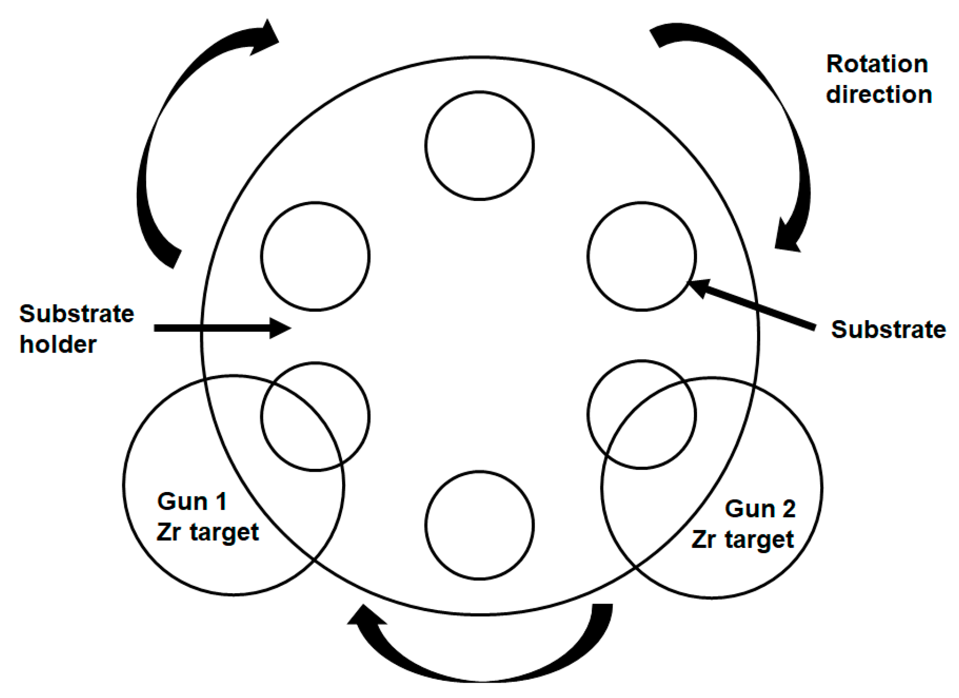
2. Materials and Methods

ZrNx films were prepared on silicon substrates through reactive DCMS. Figure 1 schematically displays the related positions of sputter targets and the samples in the sputtering chamber. A sputtering gun (gun 1) with Zr target was operated at 150 W in the sputtering process using a N2 flow ratio [f = N2/(Ar + N2)] ranging from 0.50 to 0.85 and a sputter time of 180 min. As the deposition rate decreased with increasing N2 flow ratios (Table 1), both guns 1 and 2, with powers of 150 W, were utilized for raising the deposition rate of the process with f = 1.00. Zr60N40 films prepared with an N2 flow ratio of 0.4, gun 1 power of 300 W, and sputter time of 60 min, that were reported in a previous study [30], are discussed for comparison. The diameter of Zr targets was 50.8 mm. The total flow rates of Ar and N2 were fixed at 20 sccm with a working pressure of 0.4 Pa. The target-to-substrate distance was 90 mm. The electrically-grounded substrate holder was rotated at 5 rpm.
A field-emission electron probe microanalyzer (FE-EPMA, JXA-8500F, JEOL, Akishima, Japan) was used to analyze the chemical composition of the films. The thickness of films was evaluated by field emission scanning electron microscopy (FE-SEM, S4800, Hitachi, Tokyo, Japan). An X-ray diffractometer (XRD, X’Pert PRO MPD, PANalytical, Almelo, The Netherlands) with Cu Kα radiation was used to analyze the phases of the films, using the grazing incidence technique with an incidence angle of 1°. The hardness and Young’s modulus values of films were measured using a nanoindentation tester (TI-900 Triboindenter, Hysitron, MN, USA) equipped with a Berkovich diamond probe tip, and were determined from 8 measurements based on the Oliver and Pharr method [31]. The indentation depth was 50 nm. The residual stress of the films measured by the curvature method was calculated using Stoney’s equation [32,33],
σ f t f = E S h S 2 6 ( 1 ν S ) R f
where σf is the residual stress, tf is the film thickness, ES is the Young’s modulus of Si (130.2 GPa), νS is Poisson’s ratio for Si (0.279), hS is the substrate thickness (525 μm), and Rf is the radius of the curvature of the sample. The chemical states of the constituent elements were examined by using an X-ray photoelectron spectroscope (XPS, PHI 1600, PHI, Kanagawa, Japan) with an Mg Ka X-ray beam and calibrated with the C 1s line at 284.6 eV. The nanostructure of the samples with a protective Pt layer was observed using transmission electron microscopy (TEM, JEM-2010F, JEOL, Akishima, Japan). The average surface roughness (Ra) of the films determined from 3 measurements was evaluated by using an atomic force microscope (AFM, Dimension 3100 SPM, NanoScope IIIa, Veeco, Santa Barbara, CA, USA) with a scanned area of 5 μm × 5 μm [33].

3. Results

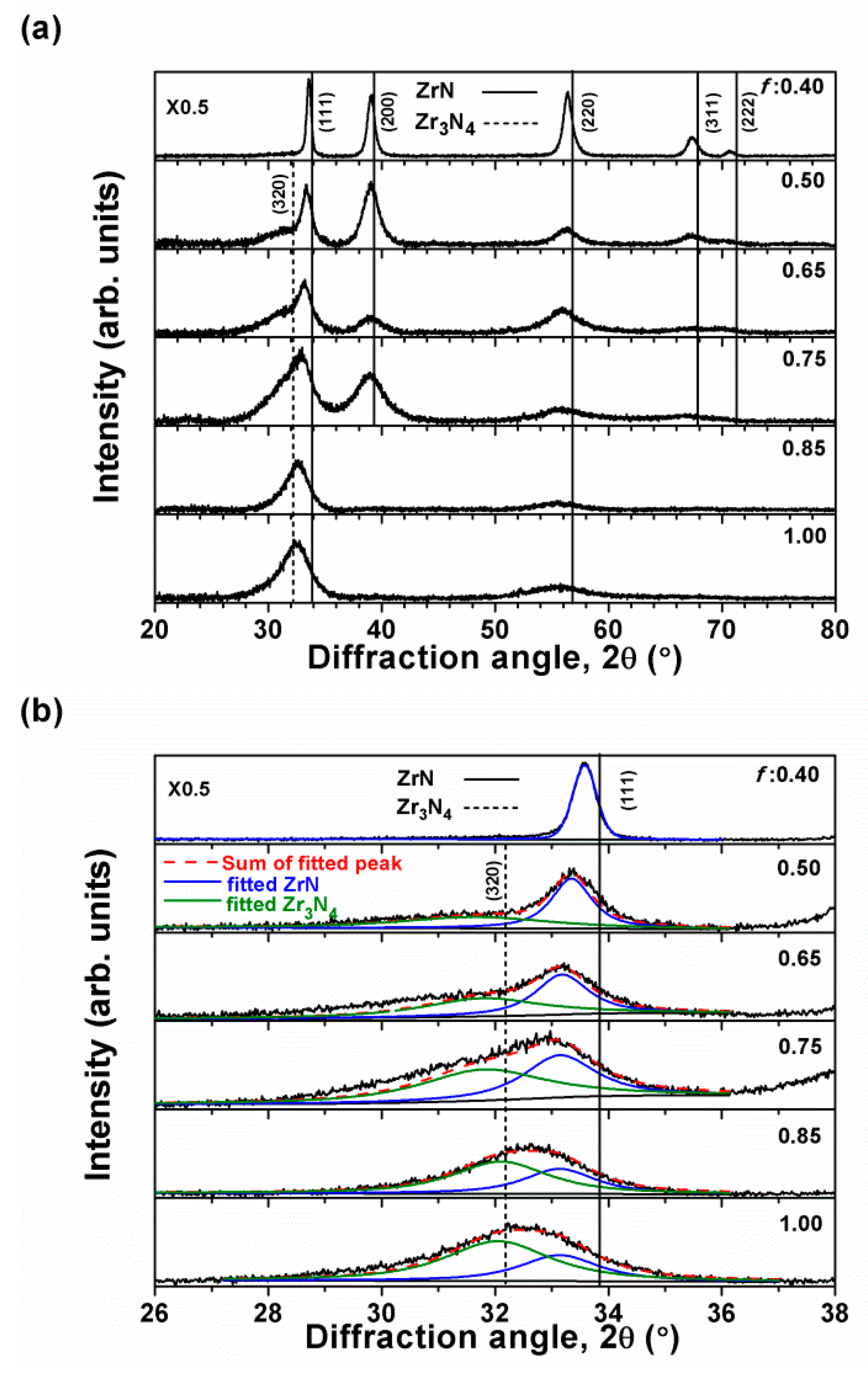
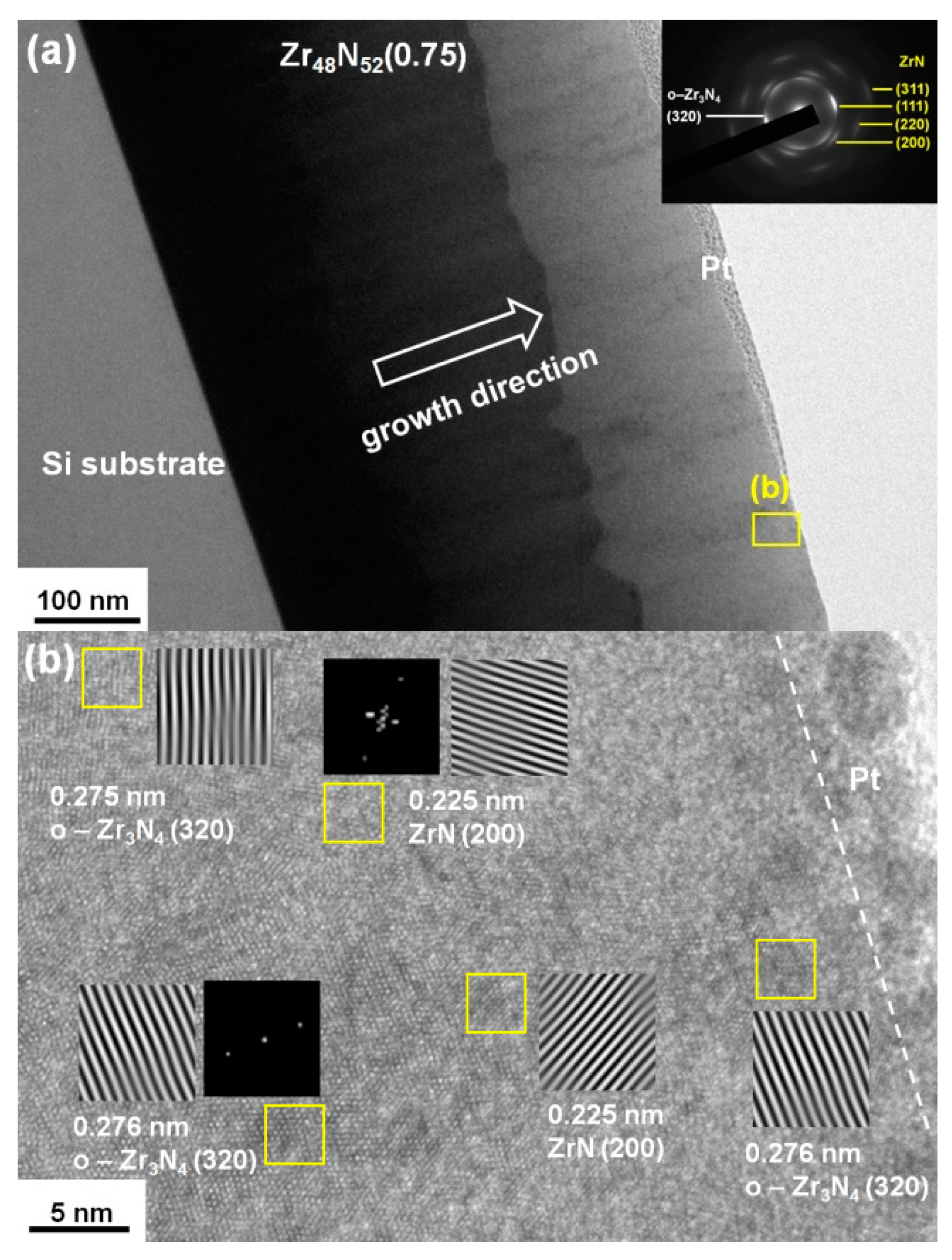
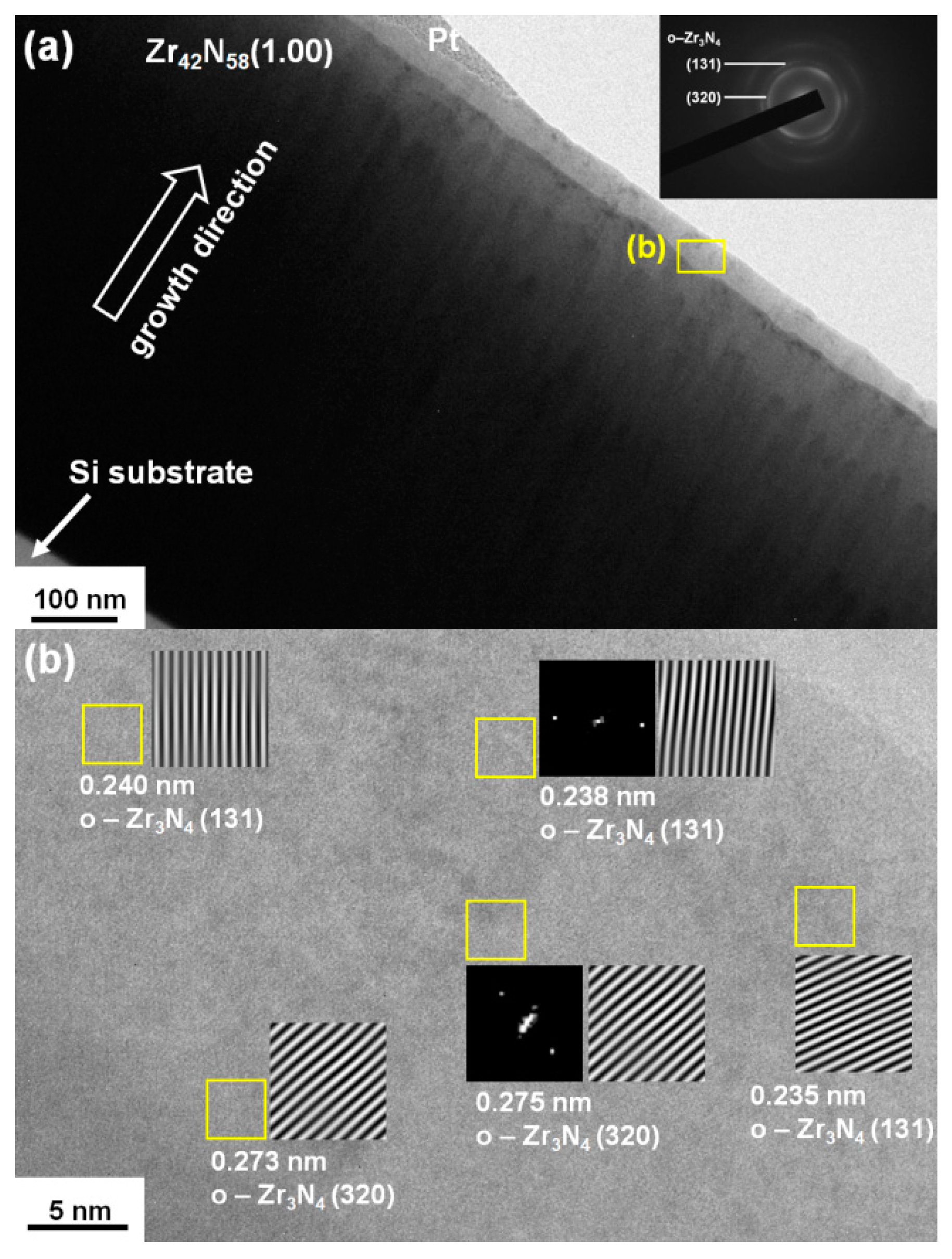
3.1. Chemical Compositions and Crystalline Phases

Table 1 lists the chemical composition of the ZrNx films fabricated with various f values. The ZrNx samples were named in the form ZryN(100−y)(f). The silicon contents were 1.5–1.8 at.% for the Zr52N48(0.50), Zr50N50(0.65), and Zr42N58(1.00) films with thicknesses of 616 to 694 nm, whereas the Zr48N52(0.75) and Zr45N55(0.85) films exhibited high Si contents of 4.8 and 10.8 at.%, respectively, which were attributed to lower thickness values of 556 and 348 nm. Therefore, the Si signals contributed by the Si substrates were observed. In our previous study [30], the Zr60N40(0.40) films prepared using the same sputter equipment with a sputter power of 300 W, N2 flow ratio of 0.4, and sputter time of 60 min exhibited a thickness of 820 nm and Si-free chemical composition. The O contents of 2 to 3 at.% in the ZrNx films were comparable with our previous study using a DCMS system [30,33]. The stoichiometric variable x increased from 0.92 to 1.00, 1.08, and 1.22 with an increasing f from 0.50 to 0.65, 0.75, and 0.85. This was accompanied by a decrease in the deposition rate from 3.8 to 3.4, 3.1, and 1.9 nm/min as only gun 1 was applied with a DC power of 150 W. The decrease in deposition rate with the increasing f level was caused by the reduced ionization and sputtering yield of N2 related to Ar gas [34]. Moreover, the well-known target poisoning effect in reactive sputtering reduced the deposition rate [34,35,36]. The Zr42N58(1.00) films prepared using an f of 1.00 and sputter power of 150 W on both guns 1 and 2 exhibited an x of 1.38 and a deposition rate of 3.9 nm/min; this deposition rate was almost twice that of the Zr45N55(0.85) films prepared with a high f level and using gun 1 only.
Figure 2a shows the XRD patterns of the ZrNx films. In a previous study [30], the XRD pattern of the Zr60N40(0.40) films exhibited a ZrN phase [ICDD 00-035-0753] with evident (111), (200), (220), (311), and (222) reflections, which are also shown in Figure 2a for comparison. Ramana et al., [35] reported that ZrN films prepared with an f < 0.28 through DCMS were crystalline. The stoichiometric variable x (N/Zr) increased by raising the f level either in DCMS [35] or hollow cathode discharge ion-plating [37]. The Zr52N48(0.50), Zr50N50(0.65), and Zr48N52(0.75) films exhibited a ZrN phase and an extra reflection identified as orthorhombic Zr3N4(320) [ICDD 00-051-0646], which was comparable with findings reported by Signore et al. [17]. The ZrN(200) reflections of the Zr60N40(0.40), Zr52N48(0.50), Zr50N50(0.65), and Zr48N52(0.75) films exhibited lattice constants of 0.4622, 0.4653, 0.4676, and 0.4682 nm, respectively, which implied that at an angle of 2θ, the ZrN(111) reflections should be 33.58°, 33.35°, 33.18°, and 33.14°, respectively; therefore, the overlapped reflections at two-theta angle at around 32°–33° were fitted as shown in Figure 2b. The ZrN(111) reflections of the Zr45N55(0.85) and Zr42N58(1.00) films, which had no ZrN(200) reflections, were positioned at 33.14°. No Zr3N4 reflection was observed for the Zr60N40(0.40) films. The intensity ratio of ZrN(111):Zr3N4(320) varied from 54:46 to 49:51, 44:56, 37:63, and 33:67 as the f value increased from 0.50 to 0.65, 0.75, 0.85, and 1.00, which implied that the phase varied from ZrN to Zr3N4-dominant as the f value increased. Figure 2a shows that the insignificant reflection at 2θ ≈ 55° for Zr45N55(0.85) and Zr42N58(1.00) films could be a combination of ZrN(220), Zr3N4(251), Zr3N4(511), and Zr3N4(002).
Figure 3a displays the cross-sectional TEM image of Zr48N52(0.75) films, which exhibit a dense structure. The selected area diffraction pattern (SADP) at the near surface region exhibited ZrN and o-Zr3N4 phases. Figure 3b displays a high-resolution TEM image of Zr48N52(0.75) films, which indicates a nanocrystalline structure comprising ZrN and o-Zr3N4 crystallites distributed randomly. The fast Fourier transform (FFT) and lattice fringes of selected regions indicated ZrN(200) and o-Zr3N4(320) crystallites with d-spacings of 0.225 and 0.276 nm, respectively. Figure 4a illustrates the cross-sectional TEM image of Zr42N58(1.00) films, which SADP is a diffused ring pattern corresponding to o-Zr3N4. Figure 4b displays the high-resolution TEM image of Zr42N58(1.00) films, whereby only o-Zr3N4 crystallites are observed.

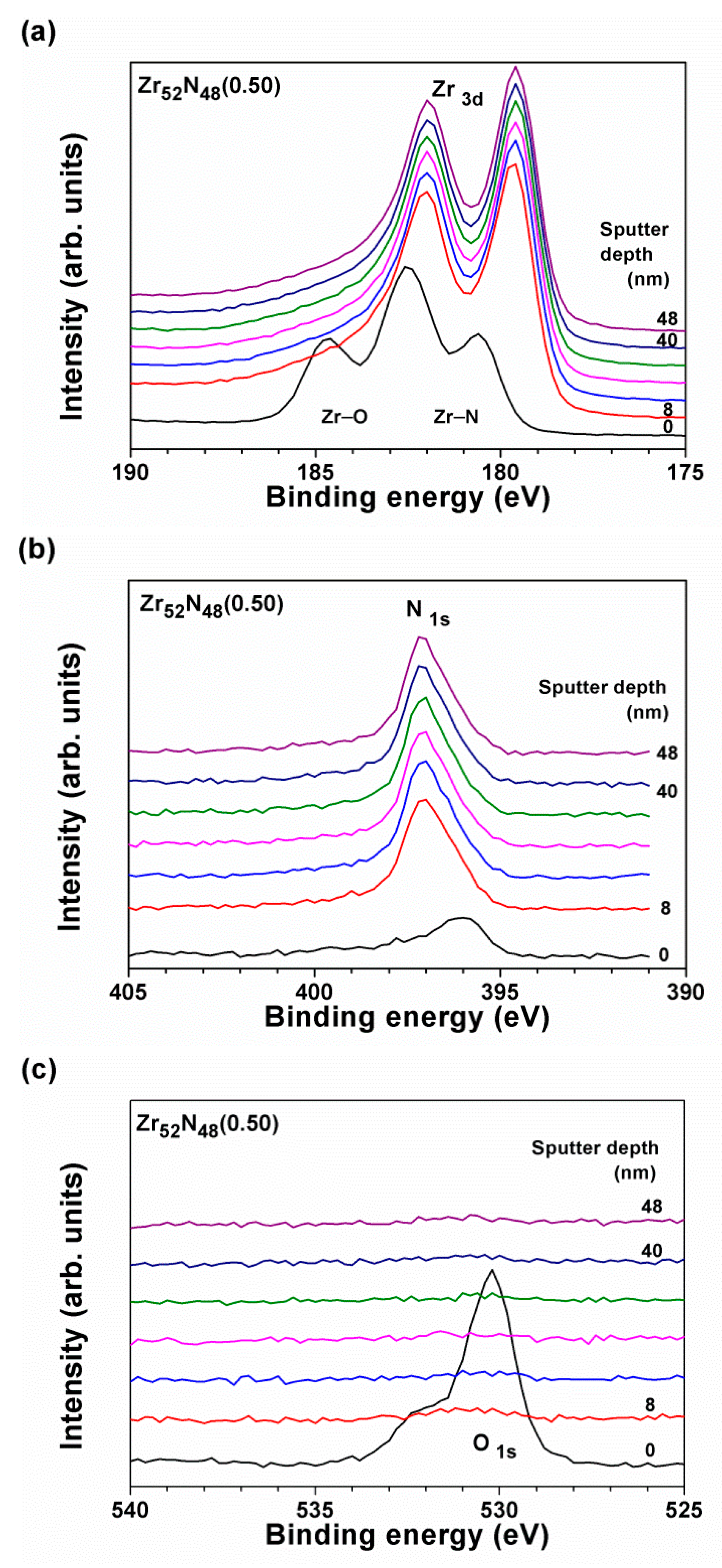
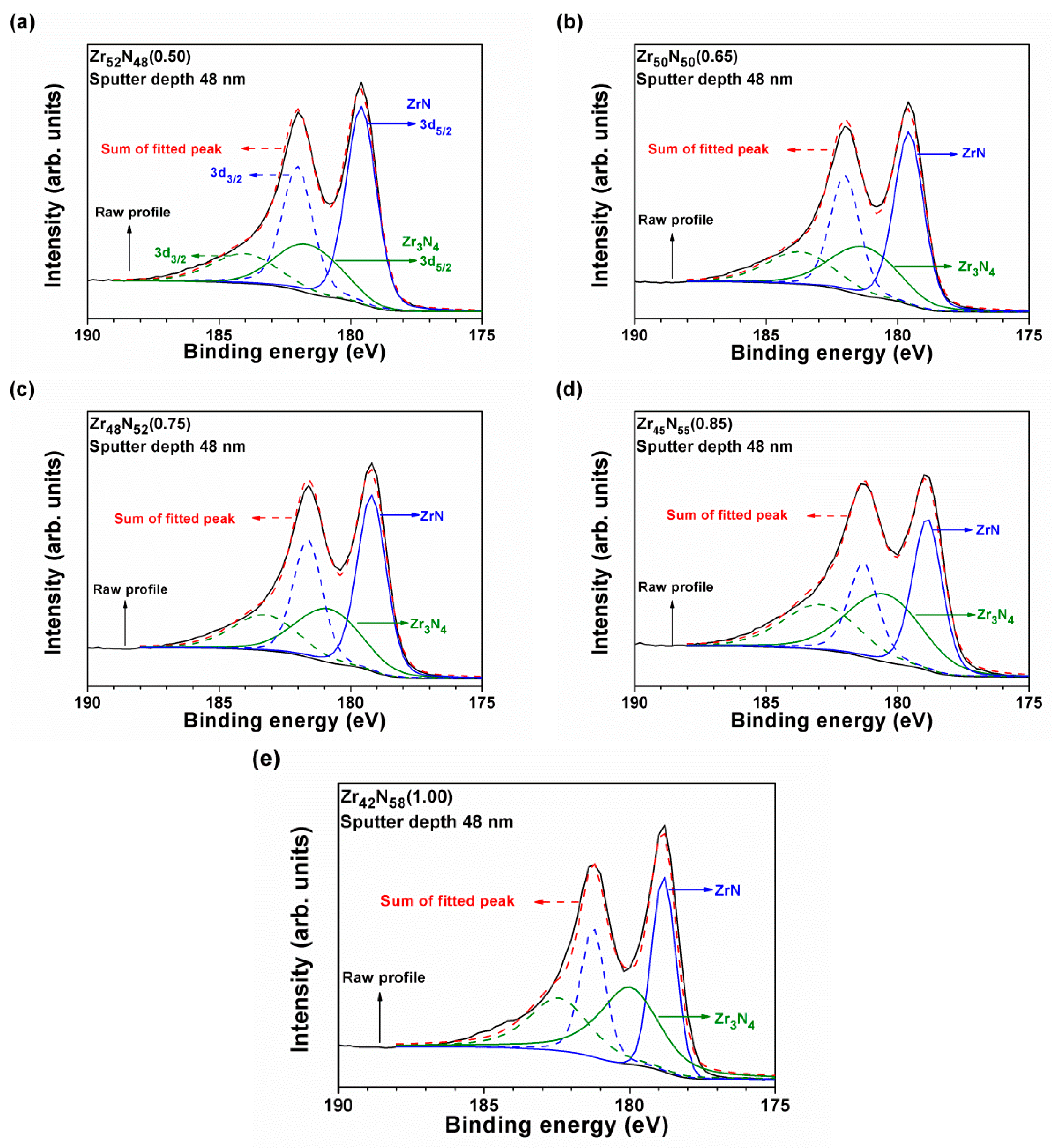
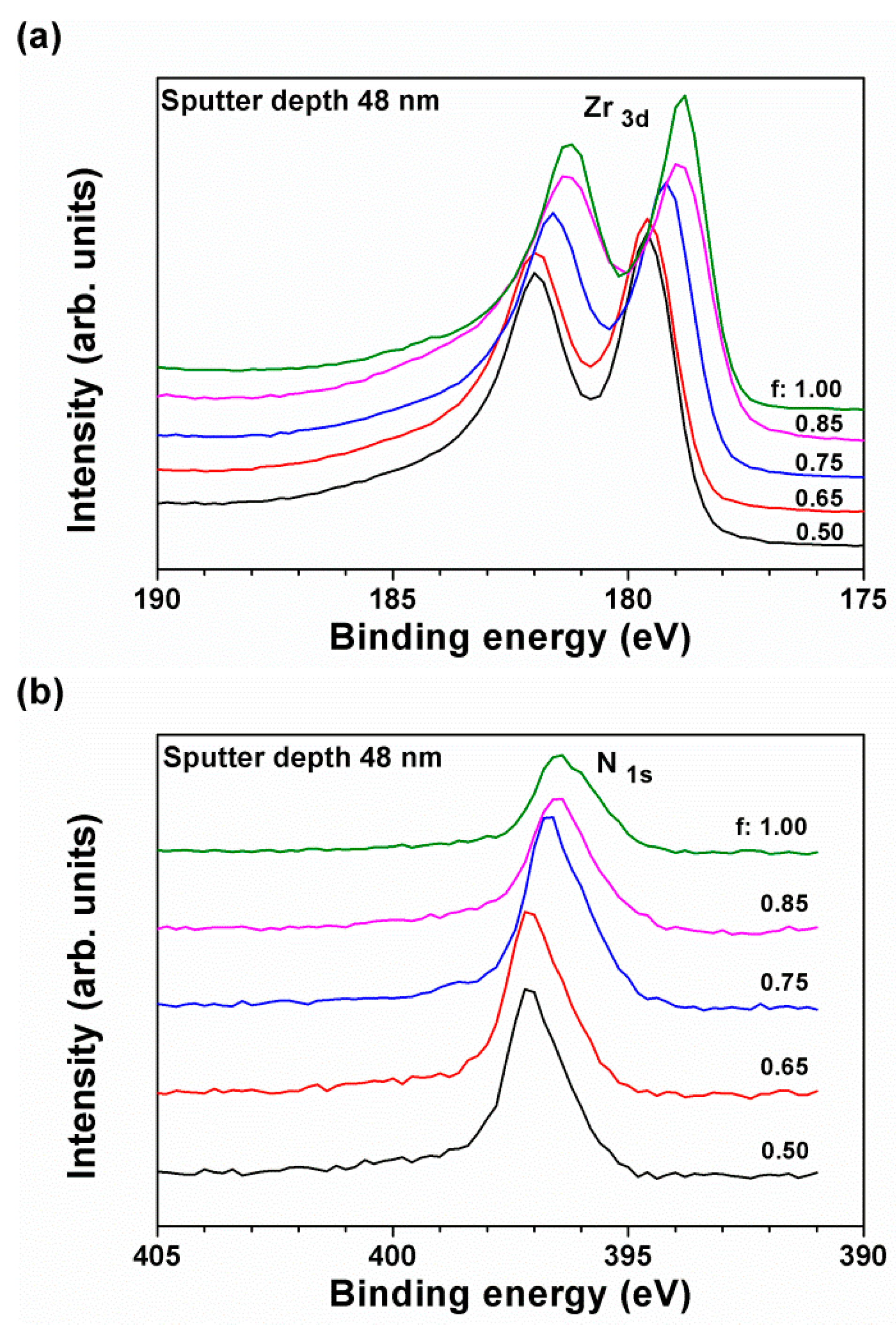
3.2. Bonding Characteristics

The correlation between XRD and XPS analyses was applied to evaluate the mixture constitution of ZrN and Zr3N4 [26,38]. Figure 5 exhibits the XPS profiles of the Zr 3d, N 1s, and O 1s core levels of the Zr52N48(0.50) films at sputter depths of 0 to 48 nm. The profiles at the free surface exhibited serious oxygen pollution because of a high affinity of Zr and O, whereas the profiles beneath the surface were not influenced by O. Figure 6 displays the curve-fitting results of the Zr 3d profiles at a sputter depth of 48 nm for the ZrNx films. The XPS profiles comprised two doublets, representing Zr–N bonds for ZrN and Zr3N4 compounds. The binding energies of the two 3d5/2 signals of the Zr52N48(0.50) films were identified as 179.62 ± 0.04 and 181.59 ± 0.03 eV at depths of 8–48 nm for Zr–N in ZrN and Zr3N4, respectively. The intensity ratio of ZrN:Zr3N4 was 67:33. In our previous study [33], the Zr–N bonds for ZrN and Zr3N4 compounds of the Zr60N40(0.40) films were identified as 179.55 and 181.39 eV, respectively. The N profiles of the Zr52N48(0.50) films at depths of 8–48 nm were fitted with two signals with binding energies of 397.16 ± 0.01 and 396.31 ± 0.02 eV, representing N–Zr bonds for ZrN and Zr3N4 compounds, respectively. Prieto et al., [24] reported the N 1s values to be 397.3 and 396.4 eV for ZrN and Zr3N4, respectively. Furthermore, Prieto et al., [24] concluded that the Zr 3d and N 1s of Zr3N4 shifted in opposite directions with respect to those of ZrN, which resulted in an increase of the binding-energy deviation of N 1s, Zr 3d and the Zr3N4 becoming an insulator.
Figure 7 exhibits the XPS profiles of the Zr 3d and N 1s core levels of the ZrNx films at a sputter depth of 48 nm. Both the Zr 3d and N 1s binding energies shifted towards lower levels with increasing N2 flow ratios. Increasing the N2 flow ratio to 1.00 decreased the 3d5/2 signal values of Zr–N bonds to 178.82 ± 0.02 and 180.06 ± 0.04 eV for ZrN and Zr3N4 compounds, respectively. Previously reported Zr 3d5/2 values of Zr–N bonds for ZrNx were 178.8–179.8 eV [39,40,41,42], whereas those of Zr–N bonds for ZrN1+x were 180.3–181.0 eV [40,41]. Table 2 lists the intensity ratios of the two 3d5/2 signals in the form ZrN:Zr3N4. The ratio of Zr–N bonds in the Zr3N4 compound increased with increasing N content in the ZrNx films, which is an accordance with the observation on phase change by XRD. The ZrNx films fabricated with an f value higher than 0.85 exhibited Zr3N4-dominant bonding structures.

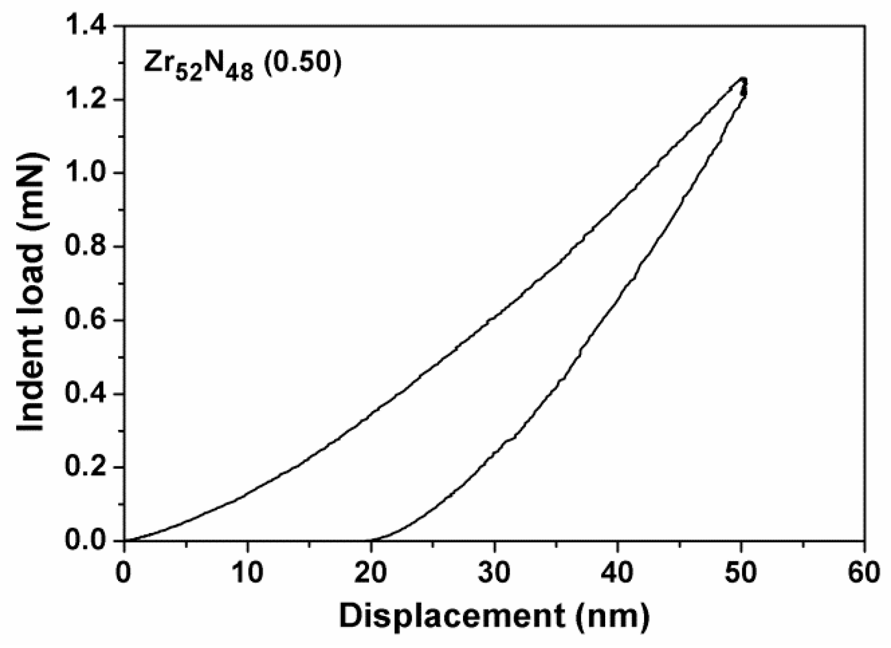
3.3. Mechanical Properties

Table 3 shows the mechanical properties of ZrNx films. The ZrNx films prepared with f levels of 0.50–1.00 exhibited insignificant variations in hardness (18.3–19.0 GPa) and Young’s modulus (210–234 GPa), although the residual stress ranged from −0.2 to −1.2 GPa. The Zr45N55(0.85) films exhibited an underestimated hardness of 17.3 GPa, which was attributed to the substrate effect because the indentation depth was 50 nm and the films possessed a low thickness of 348 nm (Table 1), which did not follow the 1/10 rule for accurate examination [43]. Figure 8 displays a representative curve of displacement against load in the nanoindentation test. The Zr60N40(0.40) films with a crystalline ZrN phase and a thickness of 820 nm exhibited a hardness of 21.0 GPa and a Young’s modulus of 248 GPa, using an indentation depth of 80 nm accompanied with a residual stress of −0.9 GPa [30]. Qi et al., [5] reported that the hardness values of magnetron-sputtered ZrN films increased from 19.74 to 34.11 GPa as the negative bias voltage changed from 0 to 100 V, resulting in an increase in compressive stress from 0.50 to 4.24 GPa and a decrease in grain size from 43.4 to 11.6 nm. Further increasing the bias voltage decreased the hardness because of the inverse Hall–Petch effect as the grain size was <10 nm. In the work of Mae et al. [44], the ZrN films fabricated without bias application exhibited a stress ranging from −1 to −2.5 GPa, corresponding to a hardness level of 16–25 GPa depending on the N2 flow rate in the reactive gas. A higher N2 flow rate produced films with a lower hardness and stress. In the works of Abadias et al. [45], magnetron-sputtered ZrN films exhibited a hardness of 21.0 GPa. Previous studies indicated that the hardness of o-Zr3N4 was similar to that of ZrN [25,46]. In summary, the hardness values of crystalline ZrN films were related to their stressed conditions. The mechanical properties of ZrNx(f) films (f = 0.50–1.00) were dominated by the o-Zr3N4 phase in a nanocrystalline form accompanied with a low compressive stress level; therefore, the Young’s modulus exhibited a slight decreasing trend and the hardness maintained a constant level as the f value increased. Moreover, the evaluation of thin film mechanical properties by nanoindentation technique was affected by the surface roughness [47]. Surface roughness reduced averages and enlarged deviations of nanoindentation hardness and Young’s modulus. All the ZrNx films exhibited a low average surface roughness of 0.7–1.2 nm (Table 3); therefore, the error in the determination of mechanical properties was negligible.

4. Conclusions

ZrNx(f) films with the stoichiometric variable x ranging from 0.67 to 1.38 were fabricated on Si substrates through reactive direct current magnetron sputtering by varying the nitrogen flow ratio f from 0.4 to 1.0. As nitrogen flow ratio increased, the crystalline structure of the investigated ZrNx films varied from a cubic ZrN phase for Zr60N40(0.40) films to a mixed nanostructure of cubic ZrN and orthorhombic Zr3N4 phases for Zr52N48(0.50), Zr50N50(0.65), and Zr48N52(0.75) films, and to a Zr3N4-dominated nanostructure for Zr45N55(0.85) and Zr42N58(1.00) films. The variation in phase from ZrN to Zr3N4-dominated, analyzed by X-ray diffraction, was consistent with the alteration in bonding characteristics examined by X-ray photoelectron spectroscopy. The hardness and Young’s modulus of Zr60N40(0.40) films were 21.0 and 248 GPa, respectively. The hardness levels of ZrNx (x = 0.92–1.38) films were 18.3 to 19.0 GPa with a negligible deviation, and the Young’s modulus of the films decreased slightly from 234 to 210 GPa, which were attributed to the formation of the nanocrystalline o-Zr3N4 constitution and the films maintained at a low compressive residual stress level ranged from −0.2 to −1.2 GPa and a low surface roughness of 0.7–1.2 nm.

Author Contributions

Conceptualization, Y.-I.C.; funding acquisition, Y.-I.C.; investigation, Y.-E.K.; project administration, Y.-I.C.; validation, Y.-E.K. and Y.-I.C.; writing—original draft, Y.-E.K.; writing—review and editing, Y.-I.C. All authors have read and agreed to the published version of the manuscript.

Funding

This research was funded by the Ministry of Science and Technology, Taiwan, Grant Nos. 106-2221-E-019-022-MY3 and 107-2813-C-019-019-E.

Acknowledgments

The authors thank Ching-Wen Tsai at the Instrumentation Center at the National Tsing Hua University for technical support with the XPS analyses. The authors thank Su-Yueh Tsai at the Instrumentation Center at the National Tsing Hua University for technical support with the FE-EPMA analyses.

Conflicts of Interest

The authors declare no conflicts of interest.

References

  1. Perry, A.J.; Georgson, M.; Sproul, W.D. Variations in the reflectance of TiN, ZrN and HfN. Thin Solid Films 1988, 157, 255–265. [Google Scholar] [CrossRef]
  2. Budke, E.; Krempel-Hesse, J.; Maidhof, H.; Schüssler, H. Decorative hard coatings with improved corrosion resistance. Surf. Coat. Technol. 1999, 112, 108–113. [Google Scholar] [CrossRef]
  3. Chou, W.J.; Yu, G.P.; Huang, J.H. Bias effect of ion-plated zirconium nitride film on Si(100). Thin Solid Films 2002, 405, 162–169. [Google Scholar] [CrossRef]
  4. Purandare, Y.P.; Ehiasarian, A.P.; Hovsepian, P.E. Structure and properties of ZrN coatings deposited by high power impulse magnetron sputtering technology. J. Vac. Sci. Technol. A 2011, 29, 011004. [Google Scholar] [CrossRef]
  5. Qi, Z.B.; Sun, P.; Zhu, F.P.; Wang, Z.C.; Peng, D.L.; Wu, C.H. The inverse Hall–Petch effect in nanocrystalline ZrN coatings. Surf. Coat. Technol. 2011, 205, 3692–3697. [Google Scholar] [CrossRef]
  6. Chang, L.C.; Chang, C.Y.; Chen, Y.I.; Kao, H.L. Mechanical properties and oxidation behavior of ZrNx thin films fabricated through high-power impulse magnetron sputtering deposition. J. Vac. Sci. Technol. A 2016, 34, 02D107. [Google Scholar] [CrossRef]
  7. Chou, W.J.; Yu, G.P.; Huang, J.H. Corrosion resistance of ZrN films on AISI 304 stainless steel substrate. Surf. Coat. Technol. 2003, 167, 59–67. [Google Scholar] [CrossRef]
  8. Xin, Y.; Liu, C.; Huo, K.; Tang, G.; Tian, X.; Chu, P.K. Corrosion behavior of ZrN/Zr coated biomedical AZ91 magnesium alloy. Surf. Coat. Technol. 2009, 203, 2554–2557. [Google Scholar] [CrossRef]
  9. Roman, D.; Bernardi, J.; Amorim, C.; Souza, F.; Spinelli, A.; Giacomelli, C.; Figueroa, C.A.; Baumvol, I.J.R.; Basso, R.L.O. Effect of deposition temperature on microstructure and corrosion resistance of ZrN thin films deposited by DC reactive magnetron sputtering. Mater. Chem. Phys. 2011, 130, 147–153. [Google Scholar] [CrossRef]
  10. Hu, C.; Guo, K.; Li, Y.; Gu, Z.; Quan, J.; Zhang, S.; Zheng, W. Optical coatings of durability based on transition metal nitrides. Thin Solid Films 2019, 688, 137339. [Google Scholar] [CrossRef]
  11. Huang, J.H.; Lau, K.W.; Yu, G.P. Effect of nitrogen flow rate on structure and properties of nanocrystalline TiN thin films produced by unbalanced magnetron sputtering. Surf. Coat. Technol. 2005, 191, 17–24. [Google Scholar] [CrossRef]
  12. Singh, A.; Kuppusami, P.; Khan, S.; Sudha, C.; Thirumurugesan, R.; Ramaseshan, R.; Divakar, R.; Mohandas, E.; Dash, S. Influence of nitrogen flow rate on microstructural and nanomechanical properties of Zr–N thin films prepared by pulsed DC magnetron sputtering. Appl. Surf. Sci. 2013, 280, 117–123. [Google Scholar] [CrossRef]
  13. Gu, Z.; Hu, C.; Huang, H.; Zhang, S.; Fan, X.; Wang, X.; Zheng, W. Identification and thermodynamic mechanism of the phase transition in hafnium nitride films. Acta Mater. 2015, 90, 59–68. [Google Scholar] [CrossRef]
  14. Balasubramanian, K.; Khare, S.V.; Gall, D. Energetics of point defects in rocksalt structure transition metal nitrides: Thermodynamic reasons for deviations from stoichiometry. Acta Mater. 2018, 159, 77–88. [Google Scholar] [CrossRef]
  15. Kroll, P. Hafnium nitride with thorium phosphide structure: Physical properties and an assessment of the Hf-N, Zr-N, and Ti-N phase diagrams at high pressures and temperatures. Phys. Rev. Lett. 2003, 90, 125501. [Google Scholar] [CrossRef] [PubMed]
  16. Signore, M.A.; Valerini, D.; Tapfer, L.; Caretto, G.; Rizzo, A. Zirconium nitride films deposited in (Ar + N2 + H2) sputtering atmosphere: Optical, structural, and electrical properties. J. Vac. Sci. Technol. A 2011, 29, 061507. [Google Scholar] [CrossRef]
  17. Lerch, M.; Füglein, E.; Wrba, J. Synthesis, Crystal structure, and high temperature behavior of Zr3N4. Z. Anorg. Allg. Chem. 1996, 622, 367–372. [Google Scholar] [CrossRef]
  18. Takeyama, M.B.; Sato, M.; Noya, A. Thermally stable ZrN/Zr3N4 bilayered barrier system for through-Si-via process. Jpn. J. Appl. Phys. 2015, 54, 05EE02. [Google Scholar] [CrossRef]
  19. Zerr, A.; Miehe, G.; Riedel, R. Synthesis of cubic zirconium and hafnium nitride having Th3P4 structure. Nat. Mater. 2003, 2, 185–189. [Google Scholar] [CrossRef]
  20. Dzivenko, D.A.; Zerr, A.; Boehler, R.; Riedel, R. Equation of state of cubic hafnium(IV) nitride having Th3P4-type structure. Solid State Commun. 2006, 139, 255–258. [Google Scholar] [CrossRef]
  21. Chihi, T.; Fatmi, M.; Ghebouli, B.; Guemmaz, M. Theoretical prediction of the structural, elastic, electronic and optical properties of Zr3N4 and Hf3N4 compounds. Solid State Sci. 2011, 13, 1414–1419. [Google Scholar] [CrossRef]
  22. Zhang, J.D.; Yang, K. Theoretical study of the thermodynamic properties of cubic Zr3N4 and Hf3N4 under high pressures. J. Alloy. Compd. 2014, 608, 90–94. [Google Scholar] [CrossRef]
  23. Mattesini, M.; Ahuja, R.; Johansson, B. Cubic Hf3N4 and Zr3N4: A class of hard materials. Phys. Rev. B 2003, 68, 184108. [Google Scholar] [CrossRef]
  24. Prieto, P.; Galán, L.; Sanz, J.M. Electronic structure of insulating zirconium nitride. Phys. Rev. B 1993, 47, 1613–1615. [Google Scholar] [CrossRef] [PubMed]
  25. Chhowalla, M.; Unalan, H.E. Thin films of hard cubic Zr3N4 stabilized by stress. Nat. Mater. 2005, 4, 317–322. [Google Scholar] [CrossRef] [PubMed]
  26. Sui, Y.; Liu, J.; Liu, B.; Wang, L.; Yao, B. Influence of flow ratio of N2 to (N2+Ar) mixture on the structure and properties of zirconium nitride films prepared by radio frequency magnetron sputtering. J. Mater. Res. 2009, 24, 3206–3212. [Google Scholar] [CrossRef]
  27. Meng, Q.N.; Wen, M.; Qu, C.Q.; Hu, C.Q.; Zheng, W.T. Preferred orientation, phase transition and hardness for sputtered zirconium nitride films grown at different substrate biases. Surf. Coat. Technol. 2011, 205, 2865–2870. [Google Scholar] [CrossRef]
  28. Norouzian, S.; Larijani, M.M.; Afzalzadeh, R. Effect of nitrogen flow ratio on structure and properties of zirconium nitride films on Si(100) prepared by ion beam sputtering. Bull. Mater. Sci. 2012, 35, 885–887. [Google Scholar] [CrossRef]
  29. Ke, Y.E.; Chen, Y.I. Mechanical properties, bonding characteristics, and thermal stability of magnetron-sputtered HfNx films. Surf. Coat. Technol. 2020, 388, 125575. [Google Scholar] [CrossRef]
  30. Oliver, W.C.; Pharr, G.M. An improved technique for determining hardness and elastic modulus using load and displacement sensing indentation experiments. J. Mater. Res. 1992, 7, 1564–1583. [Google Scholar] [CrossRef]
  31. Janssen, G.C.A.M.; Abdalla, M.M.; van Keulen, F.; Pujada, B.R.; van Venrooy, B. Celebrating the 100th anniversary of the Stoney equation for film stress: Developments from polycrystalline steel strips to single crystal silicon wafers. Thin Solid Films 2009, 517, 1858–1867. [Google Scholar] [CrossRef]
  32. Chen, Y.I.; Chang, S.C.; Chang, L.C. Oxidation resistance and mechanical properties of Zr–Si–N coatings with cyclic gradient concentration. Surf. Coat. Technol. 2017, 320, 168–173. [Google Scholar] [CrossRef]
  33. Chang, L.C.; Zheng, Y.Z.; Chen, Y.I.; Chang, S.C.; Liu, B.W. Bonding characteristics and chemical inertness of Zr–Si–N coatings with a high Si content in glass molding. Coatings 2018, 8, 181. [Google Scholar] [CrossRef] [Green Version]
  34. Ruan, J.L.; Lii, D.F.; Lu, H.H.; Chen, J.S.; Huang, J.L. Microstructural and electrical characteristics of reactively sputtered ZrNx thin films. J. Alloy. Compd. 2009, 478, 671–675. [Google Scholar] [CrossRef]
  35. Ramana, J.V.; Kumar, S.; David, C.; Ray, A.K.; Raju, V.S. Characterisation of zirconium nitride coatings prepared by DC magnetron sputtering. Mater. Lett. 2000, 43, 73–76. [Google Scholar] [CrossRef]
  36. Berg, S.; Nyberg, T. Fundamental understanding and modeling of reactive sputtering processes. Thin Solid Films 2005, 476, 215–230. [Google Scholar] [CrossRef]
  37. Huang, J.H.; Ho, C.H.; Yu, G.P. Effect of nitrogen flow rate on the structure and mechanical properties of ZrN thin films on Si(1 0 0) and stainless steel substrates. Mater. Chem. Phys. 2007, 102, 31–38. [Google Scholar] [CrossRef]
  38. Sui, Y.R.; Xu, Y.; Yao, B.; Xiao, L.; Liu, B. Preparation, characterization and properties of N-rich Zr–N thin film with Th3P4 structure. Appl. Surf. Sci. 2009, 255, 6355–6358. [Google Scholar] [CrossRef]
  39. Höchst, H.; Bringans, R.D.; Steiner, P.; Wolf, T. Photoemission study of the electronic structure of stoichiometric and substoichiometric TiN and ZrN. Phys. Rev. B 1982, 25, 7183–7191. [Google Scholar] [CrossRef]
  40. Netterfield, R.P.; Martin, P.J.; McKenzie, D.R. Properties of ZrNx prepared by ion-assisted deposition. J. Mater. Sci. Lett. 1990, 9, 972–974. [Google Scholar] [CrossRef]
  41. Bertóti, I. Characterization of nitride coatings by XPS. Surf. Coat. Technol. 2002, 151–152, 194–203. [Google Scholar] [CrossRef]
  42. Carvalho, P.; Chappé, J.M.; Cunha, L.; Lanceros-Méndez, S.; Alpuim, P.; Vaz, F.; Alves, E.; Rousselot, C.; Espinós, J.P.; González-Elipe, A.R. Influence of the chemical and electronic structure on the electrical behavior of zirconium oxynitride films. J. Appl. Phys. 2008, 103, 104907. [Google Scholar] [CrossRef] [Green Version]
  43. Saha, R.; Nix, W.D. Effects of the substrate on the determination of thin film mechanical properties by nanoindentation. Acta Mater. 2002, 50, 23–38. [Google Scholar] [CrossRef]
  44. Mae, T.; Nose, M.; Zhou, M.; Nagae, T.; Shimamura, K. The effects of Si addition on the structure and mechanical properties of ZrN thin films deposited by an r.f. reactive sputtering method. Surf. Coat. Technol. 2001, 142–144, 954–958. [Google Scholar] [CrossRef]
  45. Abadias, G.; Uglov, V.V.; Saladukhin, I.A.; Zlotski, S.V.; Tolmachova, G.; Dub, S.N.; Janse van Vuuren, A. Growth, structural and mechanical properties of magnetron-sputtered ZrN/SiNx nanolaminated coatings. Surf. Coat. Technol. 2016, 308, 158–167. [Google Scholar] [CrossRef]
  46. Ushakov, S.V.; Navrotsky, A.; Hong, Q.J.; van de Walle, A. Carbides and nitrides of zirconium and hafnium. Materials 2019, 12, 2728. [Google Scholar] [CrossRef] [Green Version]
  47. Qasmi, M.; Delobelle, P. Influence of the average roughness Rms on the precision of the Young’s modulus and hardness determination using nanoindentation technique with a Berkovich indenter. Surf. Coat. Technol. 2006, 201, 1191–1199. [Google Scholar] [CrossRef]
Figure 1. Relationship of sputter targets to the sample positions.
Coatings 10 00476 g001
Figure 2. (a) and (b) X-ray diffraction (XRD) patterns of ZrNx films prepared using various N2 flow ratios (f).
Coatings 10 00476 g002
Figure 3. (a) Cross-sectional transmission electron microscope (TEM) image and selected area diffraction pattern (SADP), and (b) a high-resolution image of the Zr48N52(0.75) films.
Coatings 10 00476 g003
Figure 4. (a) Cross-sectional TEM image and SADP, and (b) high-resolution image of the Zr42N58(1.00) films.
Coatings 10 00476 g004
Figure 5. X-ray photoelectron spectroscope (XPS) profiles of the (a) Zr 3d, (b) N 1s, and (c) O 1s core levels of the Zr52N48(0.50) films at depths of 0 to 48 nm (sputter rate = 8 nm/min for SiO2).
Coatings 10 00476 g005
Figure 6. Curve fitting of the Zr 3d signals of (a) Zr52N48(0.50), (b) Zr50N50(0.65), (c) Zr48N52(0.75), (d) Zr45N55(0.85), and (e) Zr42N58(1.00) films at depths of 48 nm.
Coatings 10 00476 g006
Figure 7. XPS profiles of the (a) Zr 3d and (b) N 1s core levels of the ZrNx films (f = 0.50–1.00) at a sputter depth of 48 nm.
Coatings 10 00476 g007
Figure 8. Typical load-displacement curve of nanoindentation tests.
Coatings 10 00476 g008
Table 1. Chemical composition and deposition rates of ZrNx films prepared using various N2 flow ratios.
SamplefaChemical Composition (at.%)xbThickness
(nm)
D c
(nm/min)
ZrNSiO
P1 d = 300 W, P2 e = 0 W
Zr60N400.4057.9 ± 0.838.8 ± 0.8-3.3 ± 0.10.6782013.7
P1 = 150 W, P2 = 0 W
Zr52N480.5049.3 ± 0.846.4 ± 1.11.6 ± 0.02.5 ± 0.20.926803.8
Zr50N500.6548.0 ± 2.047.3 ± 2.21.8 ± 0.02.8 ± 0.31.006163.4
Zr48N520.7544.1 ± 0.447.8 ± 0.34.8 ± 0.13.2 ± 0.11.085563.1
Zr45N550.8539.5 ± 1.647.5 ± 2.210.8 ± 0.42.2 ± 0.21.223481.9
P1 = 150 W, P2 = 150 W
Zr42N581.0040.5 ± 0.056.0 ± 0.21.5 ± 0.22.0 ± 0.11.386943.9
af: N2 flow ratio; b x: stoichiometric variable; c D: deposition rate; d P1: power on gun 1; e P2: power on gun 2.
Table 2. XPS binding energies and intensity ratios of XRD reflections of the ZrNx films.
SampleZr 3d5/2 (eV)
Zr–N(ZrN)
Zr–N(Zr3N4)Intensity Ratio (XPS)
ZrN:Zr3N4
Intensity Ratio (XRD)
ZrN(111):Zr3N4(320)
Zr60N40(0.40)179.55 ± 0.06181.39 ± 0.0580:20100:0
Zr52N48(0.50)179.62 ± 0.04181.59 ± 0.0367:3354:46
Zr50N50(0.65)179.59 ± 0.04181.29 ± 0.0459:4149:51
Zr48N52(0.75)179.14 ± 0.03180.74 ± 0.0556:4444:56
Zr45N55(0.85)178.84 ± 0.06180.42 ± 0.0448:5237:63
Zr42N58(1.00)178.82 ± 0.02180.06 ± 0.0444:5633:67
Table 3. Mechanical properties and surface roughness values of ZrNx films.
SampleHardness
(GPa)
Young’s Modulus
(GPa)
Stress
(GPa)
Roughness
(nm)
Zr60N40(0.40)21.0 ± 0.3248 ± 6−0.9 ± 0.21.0 ± 0.0
Zr52N48(0.50)18.9 ± 1.0228 ± 10−0.6 ± 0.11.2 ± 0.0
Zr50N50(0.65)19.0 ± 0.5234 ± 6−0.2 ± 0.21.0 ± 0.1
Zr48N52(0.75)18.8 ± 0.9228 ± 5−0.5 ± 0.10.7 ± 0.0
Zr45N55(0.85)17.3 ± 0.4211 ± 3−0.7 ± 0.20.8 ± 0.1
Zr42N58(1.00)18.3 ± 0.9210 ± 5−1.2 ± 0.11.0 ± 0.0

