An Aptamer-Functionalised Schottky-Field Effect Transistor for the Detection of Proteins

Abstract
:1. Introduction
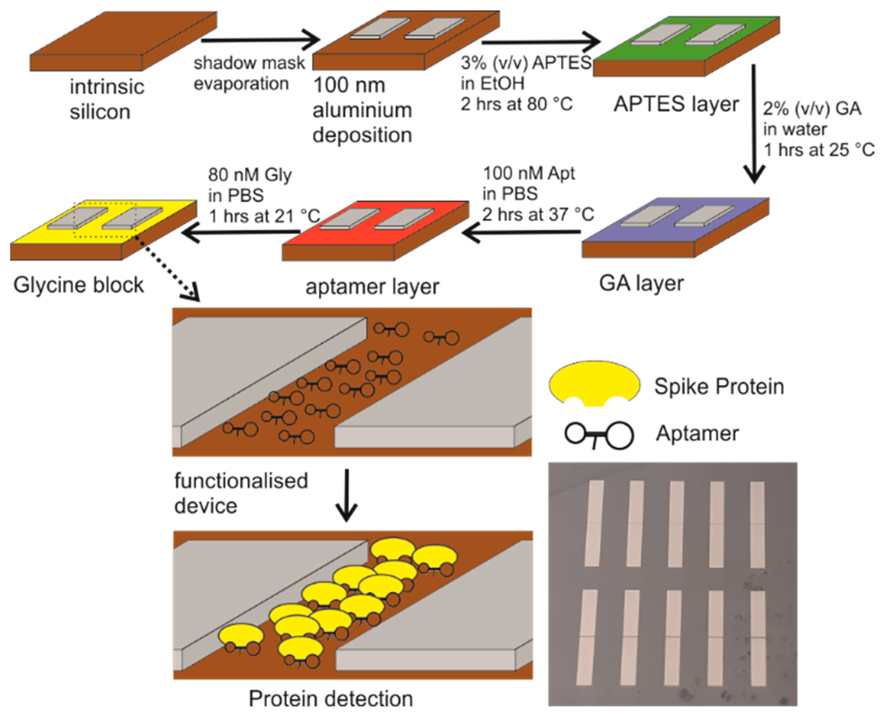
2. Materials and Methods
3. Results
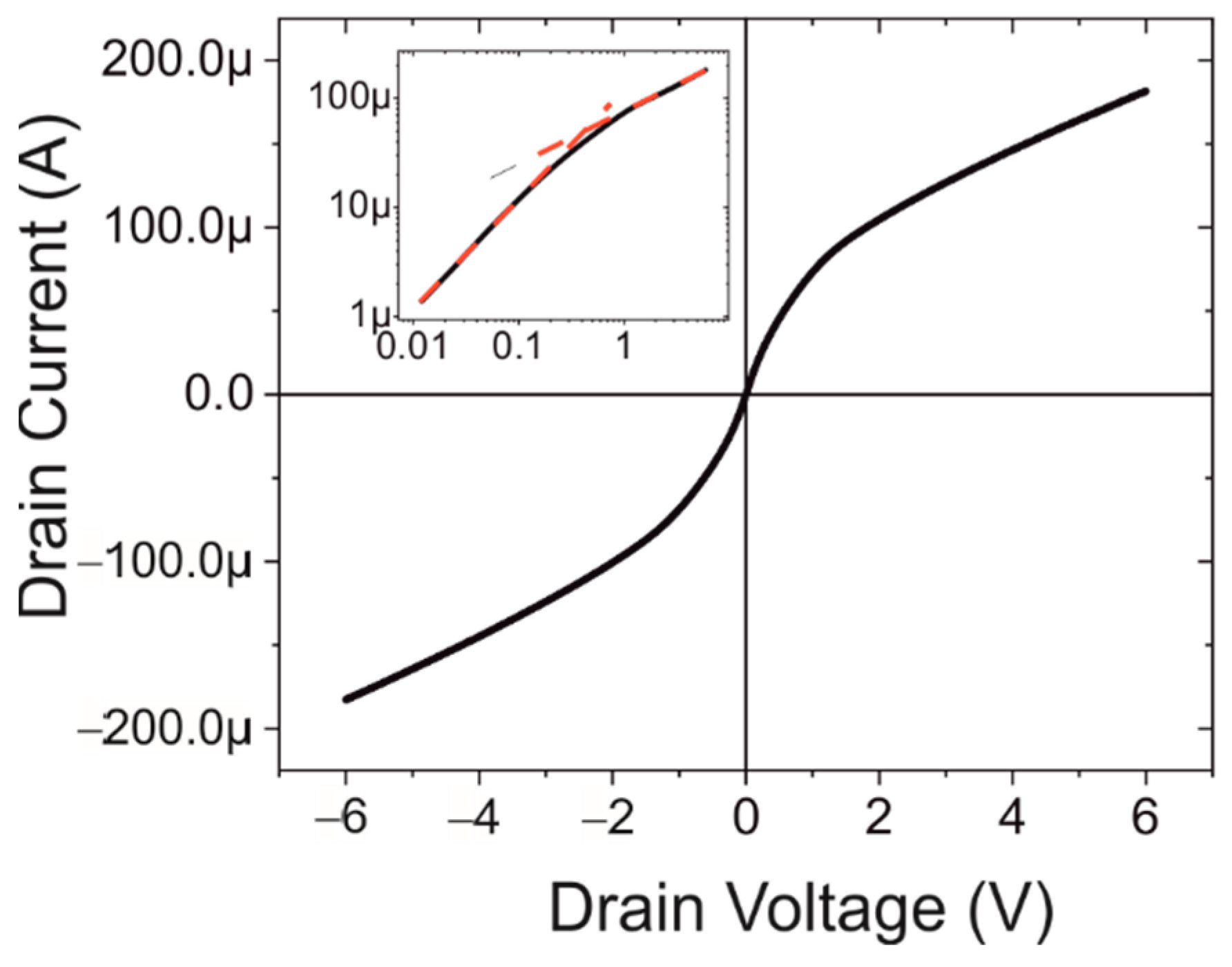
3.1. Basic Device Characterisation
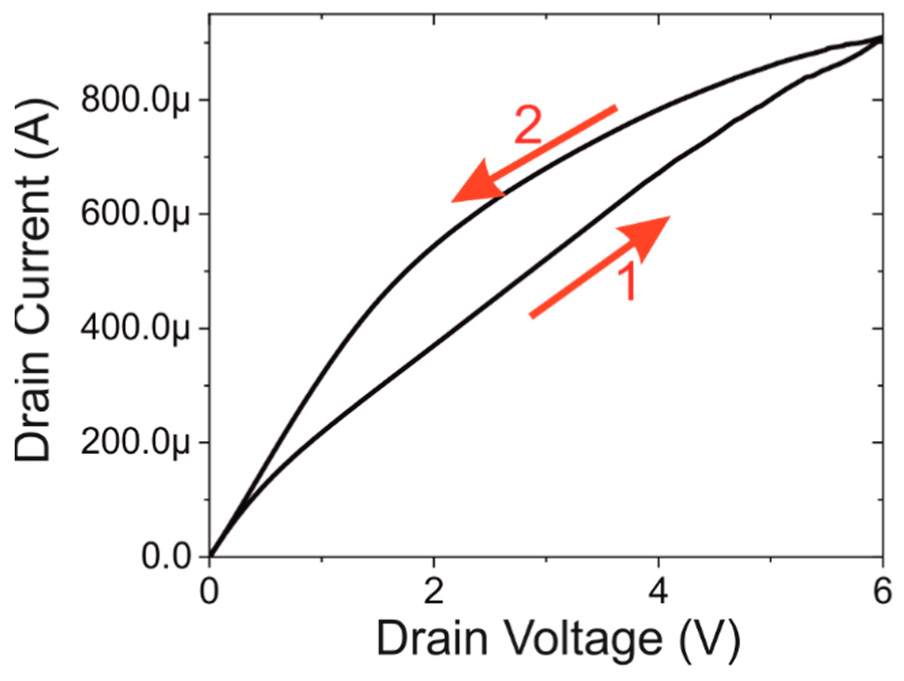
3.2. IV-Characteristics of Functionalised Devices
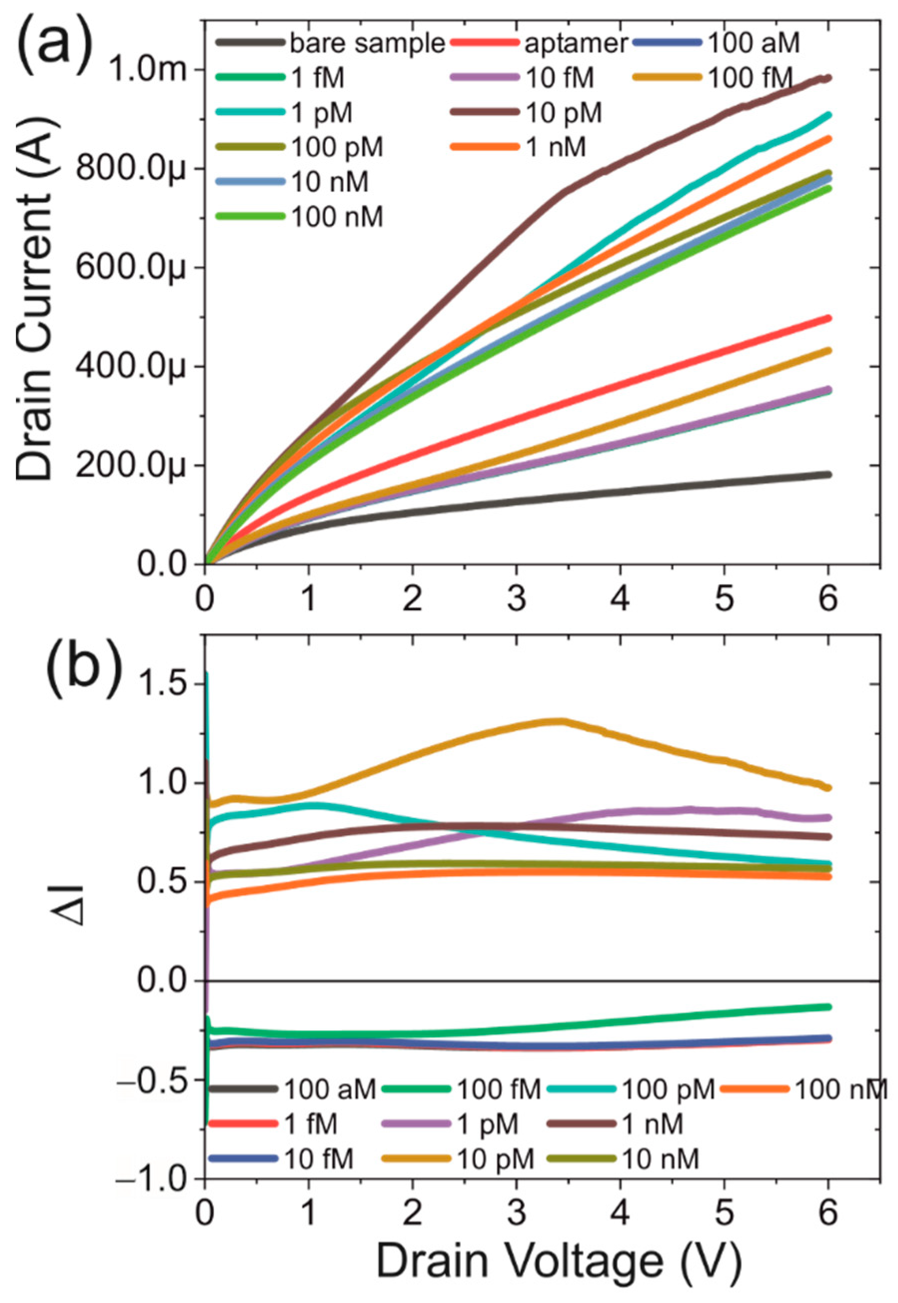
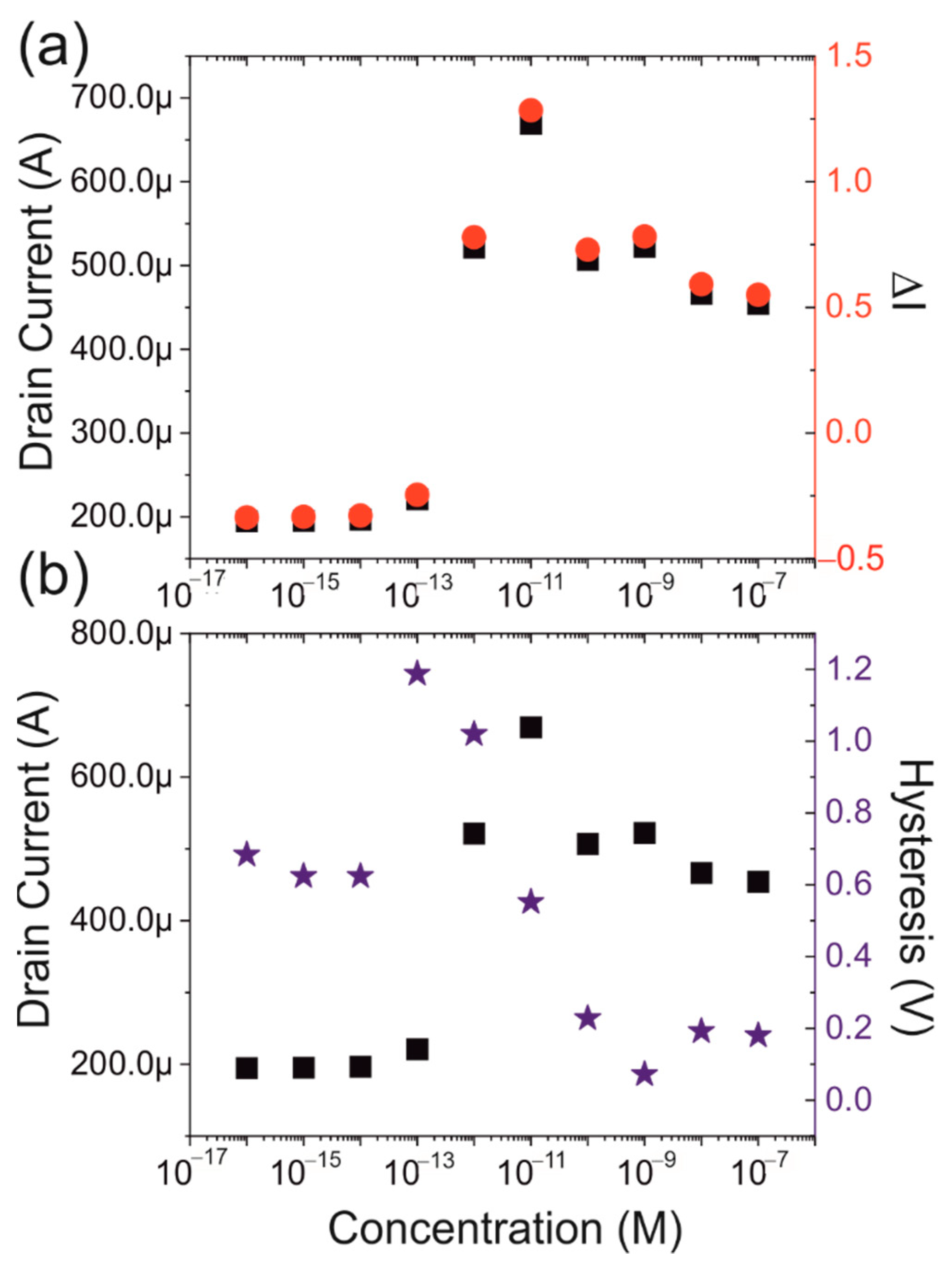
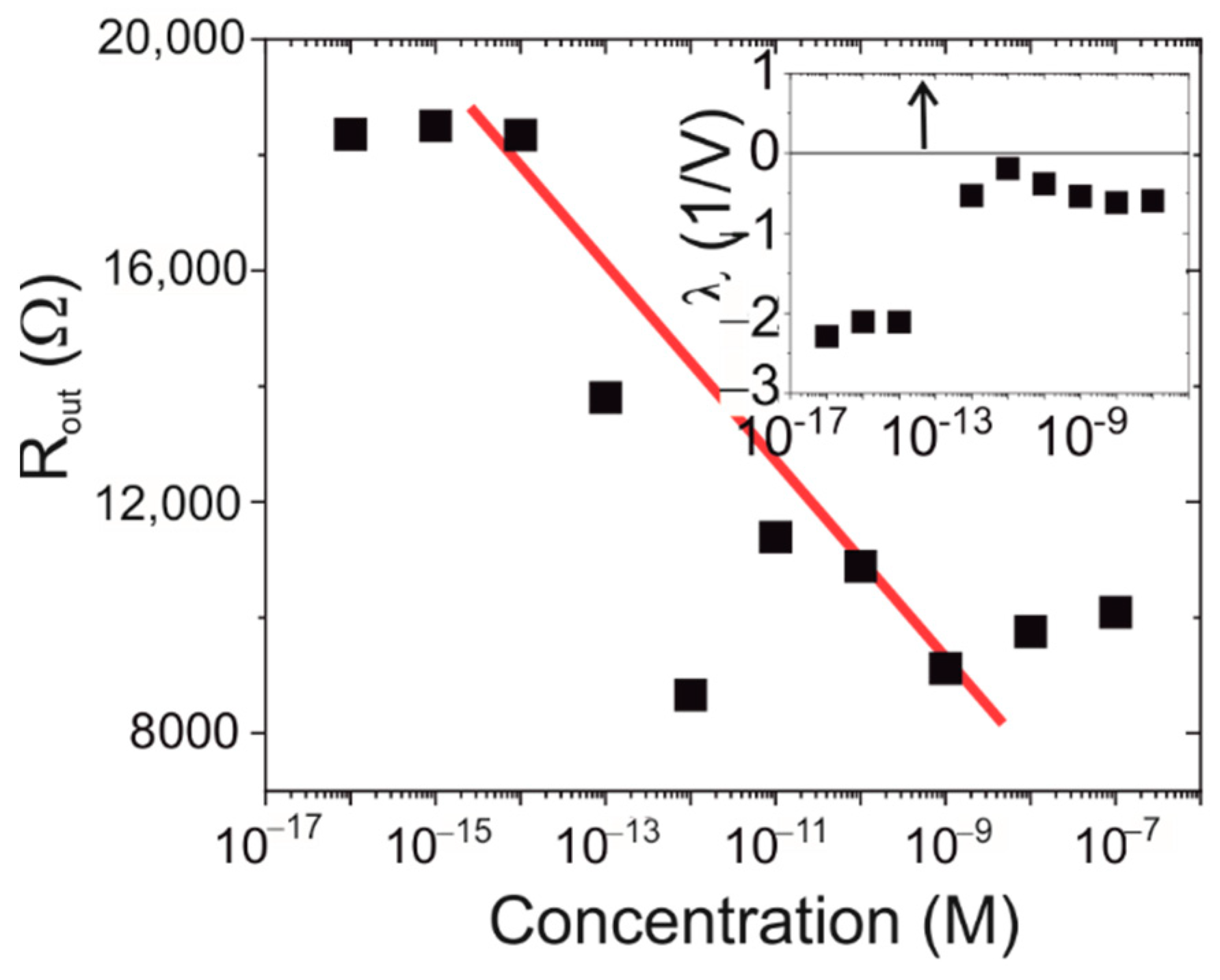
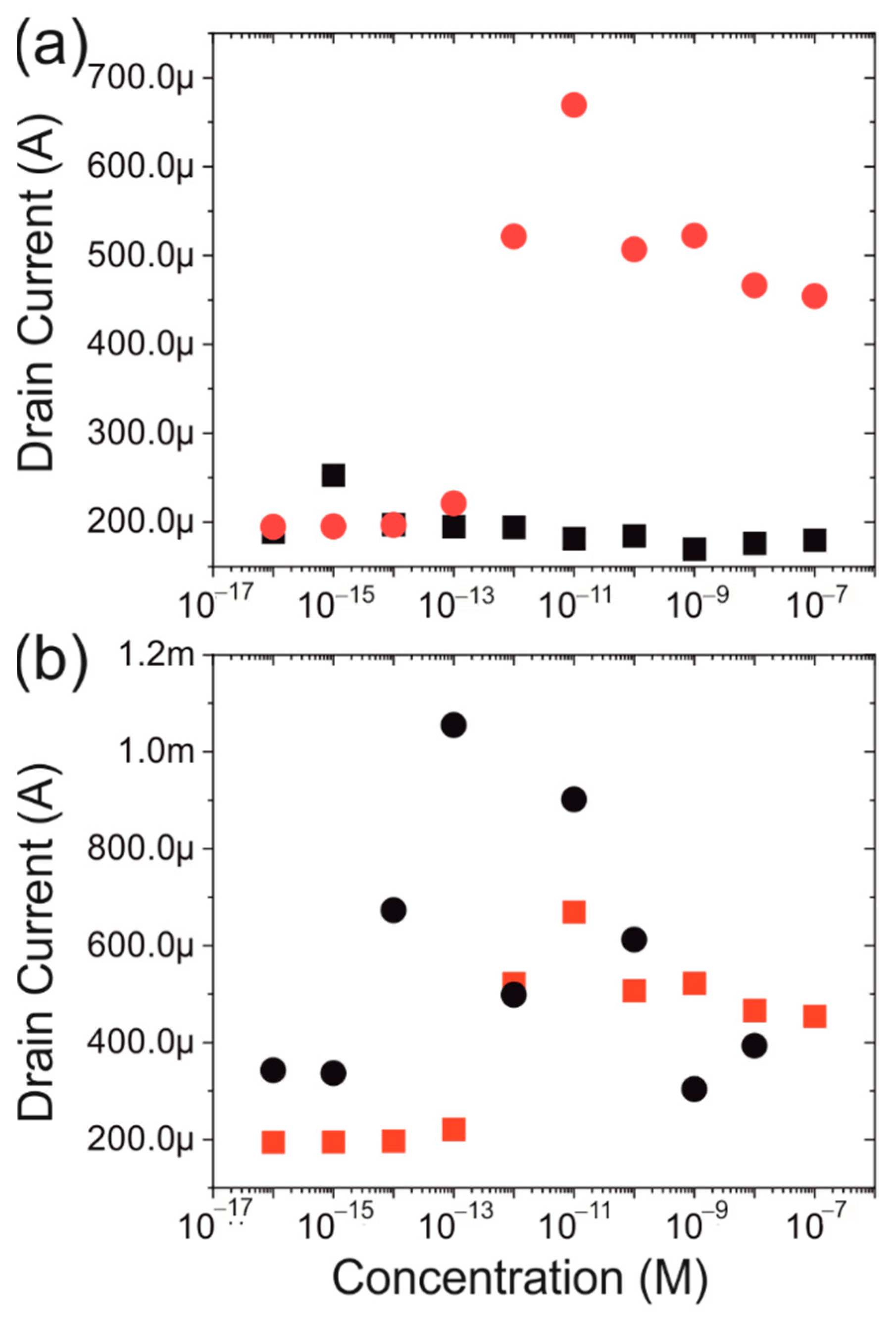
3.3. Protein Dependence
3.4. Controls
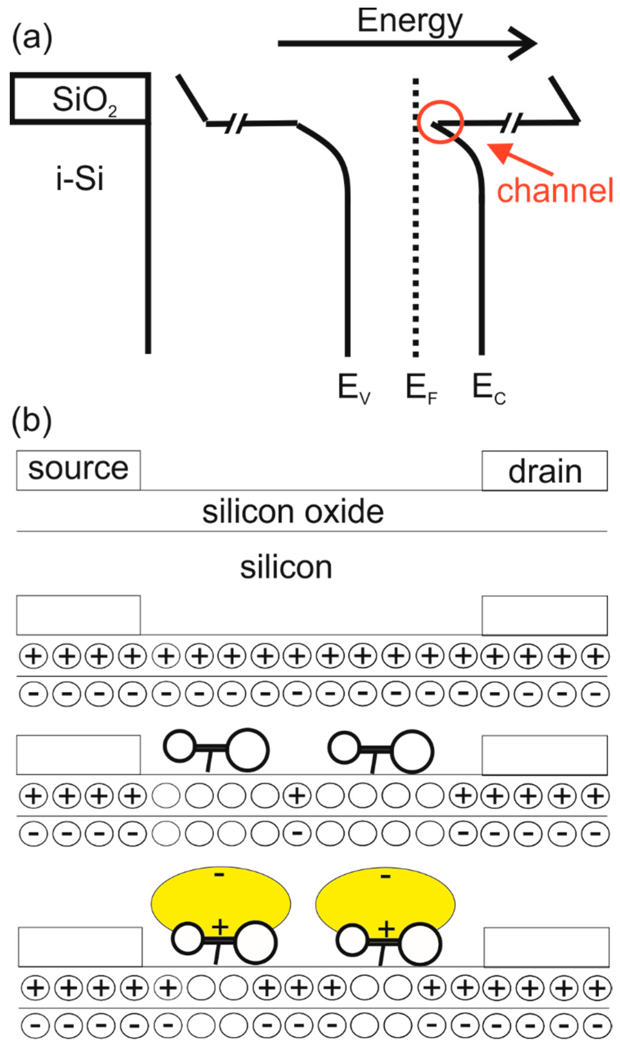
4. Discussion
5. Conclusions
Supplementary Materials
Author Contributions
Funding
Institutional Review Board Statement
Informed Consent Statement
Data Availability Statement
Conflicts of Interest
References
- World Health Organisation. Novel Coronavirus(2019-nCoV)SITUATION REPORT-121 JANUARY 2020. Available online: https://www.who.int/docs/default-source/coronaviruse/situation-reports/20200121-sitrep-1-2019-ncov.pdf (accessed on 17 January 2022).
- Gorbalenya, A.E.; Baker, S.C.; Baric, R.S.; de Groot, R.J.; Drosten, C.; Gulyaeva, A.A.; Haagmans, B.L.; Lauber, C.; Leontovich, A.M.; Neuman, B.W.; et al. The species Severe acute respiratory syndrome-related coronavirus: Classifying 2019-nCoV and naming it SARS-CoV-2. Nat. Microbiol. 2020, 5, 536–544. [Google Scholar] [CrossRef] [Green Version]
- Carter, L.J.; Garner, L.V.; Smoot, J.W.; Li, Y.; Zhou, Q.; Saveson, C.J.; Sasso, J.M.; Gregg, A.C.; Soares, D.J.; Beskid, T.R.; et al. Assay Techniques and Test Development for COVID-19 Diagnosis. ACS Cent. Sci. 2020, 6, 591–605. [Google Scholar] [CrossRef] [PubMed]
- Patolsky, F.; Zheng, G.; Hayden, O.; Lakadamyali, M.; Zhuang, X.; Lieber, C.M. Electrical detection of single viruses. Proc. Natl. Acad. Sci. USA 2004, 101, 14017–14022. [Google Scholar] [CrossRef] [PubMed] [Green Version]
- Zhang, G.J.; Zhang, L.; Huang, M.J.; Luo, Z.H.H.; Tay, G.K.I.; Lim, E.J.A.; Kang, T.G.; Chen, Y. Silicon nanowire biosensor for highly sensitive and rapid detection of Dengue virus. Sens. Actuators B Chem. 2010, 146, 138–144. [Google Scholar] [CrossRef]
- Chen, P.H.; Huang, C.C.; Wu, C.C.; Chen, P.H.; Tripathi, A.; Wang, Y.L. Saliva-based COVID-19 detection: A rapid antigen test of SARS-CoV-2 nucleocapsid protein using an electrical-double-layer gated field-effect transistor-based biosensing system. Sens. Actuators B Chem. 2022, 357, 131415. [Google Scholar] [CrossRef]
- Lin, Y.H.; Han, Y.; Sharma, A.; AlGhamdi, W.S.; Liu, C.H.; Chang, T.H.; Xiao, X.W.; Lin, W.Z.; Lu, P.Y.; Seitkhan, A.; et al. A Tri-Channel Oxide Transistor Concept for the Rapid Detection of Biomolecules Including the SARS-CoV-2 Spike Protein. Adv. Mater. 2022, 34, 2104608. [Google Scholar] [CrossRef]
- Seo, G.; Lee, G.; Kim, M.J.; Baek, S.H.; Choi, M.; Ku, K.B.; Lee, C.S.; Jun, S.; Park, D.; Kim, H.G.; et al. Rapid Detection of COVID-19 Causative Virus (SARS-CoV-2) in Human Nasopharyngeal Swab Specimens Using Field-Effect Transistor-Based Biosensor. ACS Nano 2020, 14, 5135–5142. [Google Scholar] [CrossRef] [Green Version]
- Zamzami, M.A.; Rabbani, G.; Ahmad, A.; Basalah, A.A.; Al-Sabban, W.H.; Nate Ahn, S.; Choudhry, H. Carbon nanotube field-effect transistor (CNT-FET)-based biosensor for rapid detection of SARS-CoV-2 (COVID-19) surface spike protein S1. Bioelectrochemistry 2022, 143, 107982. [Google Scholar] [CrossRef]
- Shao, W.; Shurin, M.R.; Wheeler, S.E.; He, X.; Star, A. Rapid Detection of SARS-CoV-2 Antigens Using High-Purity Semiconducting Single-Walled Carbon Nanotube-Based Field-Effect Transistors. ACS Appl. Mater. Interfaces 2021, 13, 10321–10327. [Google Scholar] [CrossRef]
- Fathi-Hafshejani, P.; Azam, N.; Wang, L.; Kuroda, M.A.; Hamilton, M.C.; Hasim, S.; Mahjouri-Samani, M. Two-Dimensional-Material-Based Field-Effect Transistor Biosensor for Detecting COVID-19 Virus (SARS-CoV-2). ACS Nano 2021, 15, 11461–11469. [Google Scholar] [CrossRef]
- Gao, J.; Wang, C.; Chu, Y.; Han, Y.; Gao, Y.; Wang, Y.; Wang, C.; Liu, H.; Han, L.; Zhang, Y. Graphene oxide-graphene Van der Waals heterostructure transistor biosensor for SARS-CoV-2 protein detection. Talanta 2022, 240, 123197. [Google Scholar] [CrossRef] [PubMed]
- Kim, J.; Jeong, S.; Sarawut, S.; Kim, H.; Son, S.U.; Lee, S.; Rabbani, G.; Kwon, H.; Lim, E.K.; Ahn, S.N.; et al. An immunosensor based on a high performance dual-gate oxide semiconductor thin-film transistor for rapid detection of SARS-CoV-2. Lab A Chip 2022, 22, 899–907. [Google Scholar] [CrossRef] [PubMed]
- Li, Y.; Peng, Z.; Holl, N.J.; Hassan, M.R.; Pappas, J.M.; Wei, C.; Izadi, O.H.; Wang, Y.; Dong, X.; Wang, C.; et al. MXene-Graphene Field-Effect Transistor Sensing of Influenza Virus and SARS-CoV-2. ACS Omega 2021, 6, 6643–6653. [Google Scholar] [CrossRef] [PubMed]
- Chiu, C.W.; Xian, M.; Stephany, J.L.; Xia, X.; Chiang, C.C.; Ren, F.; Tsai, C.T.; Shan, S.S.; Liao, Y.T.; Esquivel-Upshaw, J.F.; et al. Rapid SARS-CoV-2 diagnosis using disposable strips and a metal-oxide-semiconductor field-effect transistor platform. J. Vac. Sci. Technol. B Nanotechnol. Microelectron. 2022, 40, 023204. [Google Scholar] [CrossRef]
- Tran, D.P.; Winter, M.A.; Wolfrum, B.; Stockmann, R.; Yang, C.T.; Pourhassan-Moghaddam, M.; Offenhaüsser, A.; Thierry, B. Toward Intraoperative Detection of Disseminated Tumor Cells in Lymph Nodes with Silicon Nanowire Field Effect Transistors. ACS Nano 2016, 10, 2357–2364. [Google Scholar] [CrossRef] [Green Version]
- Ilgu, M.; Nilsen-Hamilton, M. Aptamers in analytics. Analyst 2016, 141, 1551–1558. [Google Scholar] [CrossRef] [Green Version]
- Wilson, R.; Bourne, C.; Chaudhuri, R.R.; Gregory, R.; Kenny, J.; Cossins, A. Single-step selection of bivalent aptamers validated by comparison with SELEX using high-throughput sequencing. PLoS ONE 2014, 9, e100572. [Google Scholar] [CrossRef] [Green Version]
- White, R.J.; Phares, N.; Lubin, A.A.; Xiao, Y.; Plaxco, K.W. Optimization of Electrochemical Aptamer-Based Sensors via Optimization of Probe Packing Density and Surface Chemistry. Langmuir 2008, 24, 10513–10518. [Google Scholar] [CrossRef] [Green Version]
- Song, S.; Wang, L.; Li, J.; Fan, C.; Zhao, J. Aptamer-based biosensors. TrAC-Trends Anal. Chem. 2008, 27, 108–117. [Google Scholar] [CrossRef]
- Willner, I.; Zayats, M. Electronic aptamer-based sensors. Angew. Chem.-Int. Ed. 2007, 46, 6408–6418. [Google Scholar] [CrossRef]
- Lasserre, P.; Balansethupathy, B.; Vezza, V.J.; Butterworth, A.; Macdonald, A.; Blair, E.O.; McAteer, L.; Hannah, S.; Ward, A.C.; Hoskisson, P.A.; et al. SARS-CoV-2 Aptasensors Based on Electrochemical Impedance Spectroscopy and Low-Cost Gold Electrode Substrates. Anal. Chem. 2022, 94, 2126–2133. [Google Scholar] [CrossRef] [PubMed]
- Shi, L.; Wang, L.; Ma, X.; Fang, X.; Xiang, L.; Yi, Y.; Li, J.; Luo, Z.; Li, G. Aptamer-Functionalized Nanochannels for One-Step Detection of SARS-CoV-2 in Samples from COVID-19 Patients. Anal. Chem. 2021, 93, 16646–16654. [Google Scholar] [CrossRef] [PubMed]
- Abrego-Martinez, J.C.; Jafari, M.; Chergui, S.; Pavel, C.; Che, D.; Siaj, M. Aptamer-based electrochemical biosensor for rapid detection of SARS-CoV-2: Nanoscale electrode-aptamer-SARS-CoV-2 imaging by photo-induced force microscopy. Biosens. Bioelectron. 2022, 195, 113595. [Google Scholar] [CrossRef] [PubMed]
- Vu, C.A.; Chen, W.Y. Predicting future prospects of aptamers in field-effect transistor biosensors. Molecules 2020, 25, 680. [Google Scholar] [CrossRef] [PubMed] [Green Version]
- Kwon, J.; Lee, Y.; Lee, T.; Ahn, J.H. Aptamer-Based Field-Effect Transistor for Detection of Avian Influenza Virus in Chicken Serum. Anal. Chem. 2020, 92, 5524–5531. [Google Scholar] [CrossRef]
- Nakatsuka, N.; Yang, K.A.; Abendroth, J.M.; Cheung, K.M.; Xu, X.; Yang, H.; Zhao, C.; Zhu, B.; Rim, Y.S.; Yang, Y.; et al. Aptamer-field-effect transistors overcome Debye length limitations for small-molecule sensing. Science 2018, 362, 319–324. [Google Scholar] [CrossRef]
- Syu, Y.C.; Hsu, W.E.; Lin, C.T. Review-field-effect transistor biosensing: Devices and clinical applications. ECS J. Solid State Sci. Technol. 2018, 7, Q3196–Q3207. [Google Scholar] [CrossRef]
- de Moraes, A.C.M.; Kubota, L.T. Recent trends in field-effect transistors-based immunosensors. Chemosensors 2016, 4, 20. [Google Scholar] [CrossRef] [Green Version]
- Lung Khung, Y.; Narducci, D. Synergizing nucleic acid aptamers with 1-dimensional nanostructures as label-free field-effect transistor biosensors. Biosens. Bioelectron. 2013, 50, 278–293. [Google Scholar] [CrossRef]
- Stefano, L.D.; Oliviero, G.; Amato, J.; Borbone, N.; Piccialli, G.; Mayol, L.; Rendina, I.; Terracciano, M.; Rea, I. Aminosilane functionalizations of mesoporous oxidized silicon for oligonucleotide synthesis and detection. J. R. Soc. Interface 2013, 10, 20130160. [Google Scholar] [CrossRef] [Green Version]
- Song, Y.; Song, J.; Wei, X.; Huang, M.; Sun, M.; Zhu, L.; Lin, B.; Shen, H.; Zhu, Z.; Yang, C. Discovery of Aptamers Targeting the Receptor-Binding Domain of the SARS-CoV-2 Spike Glycoprotein. Anal. Chem. 2020, 92, 9895–9900. [Google Scholar] [CrossRef] [PubMed]
- Lan, J.; Ge, J.; Yu, J.; Shan, S.; Zhou, H.; Fan, S.; Zhang, Q.; Shi, X.; Wang, Q.; Zhang, L.; et al. Structure of the SARS-CoV-2 spike receptor-binding domain bound to the ACE2 receptor. Nature 2020, 581, 215–220. [Google Scholar] [CrossRef] [Green Version]
- Kobayashi, K.; Teramoto, A.; Miyoshi, H. Origin of positive charge generated in thin SiO2 films during high-field electrical stress. IEEE Trans. Electron Devices 1999, 46, 947–953. [Google Scholar] [CrossRef]
- Sajedi Alvar, M.; Blom, P.W.M.; Wetzelaer, G.J.A.H. Space-charge-limited electron and hole currents in hybrid organic-inorganic perovskites. Nat. Commun. 2020, 11, 4023. [Google Scholar] [CrossRef] [PubMed]
- Sui, Y.; Appenzeller, J. Screening and interlayer coupling in multilayer graphene field-effect transistors. Nano Lett. 2009, 9, 2973–2977. [Google Scholar] [CrossRef] [Green Version]
- Majee, A.K.; Foss, C.J.; Aksamija, Z. Electrical and electrothermal properties of few-layer 2D devices. J. Comput. Electron. 2021, 20, 2–12. [Google Scholar] [CrossRef]
- Sheridan, C. Coronavirus testing finally gathers speed. Nat. Biotechnol. 2020. [Google Scholar] [CrossRef]


Publisher’s Note: MDPI stays neutral with regard to jurisdictional claims in published maps and institutional affiliations. |
© 2022 by the authors. Licensee MDPI, Basel, Switzerland. This article is an open access article distributed under the terms and conditions of the Creative Commons Attribution (CC BY) license (https://creativecommons.org/licenses/by/4.0/).
Share and Cite
Farrow, T.; Laumier, S.; Sandall, I.; van Zalinge, H. An Aptamer-Functionalised Schottky-Field Effect Transistor for the Detection of Proteins. Biosensors 2022, 12, 347. https://doi.org/10.3390/bios12050347
Farrow T, Laumier S, Sandall I, van Zalinge H. An Aptamer-Functionalised Schottky-Field Effect Transistor for the Detection of Proteins. Biosensors. 2022; 12(5):347. https://doi.org/10.3390/bios12050347
Chicago/Turabian StyleFarrow, Thomas, Siriny Laumier, Ian Sandall, and Harm van Zalinge. 2022. "An Aptamer-Functionalised Schottky-Field Effect Transistor for the Detection of Proteins" Biosensors 12, no. 5: 347. https://doi.org/10.3390/bios12050347