Sensitivity Enhancement of Hybrid Two-Dimensional Nanomaterials-Based Surface Plasmon Resonance Biosensor

 , ,
, ,
Abstract
:1. Introduction
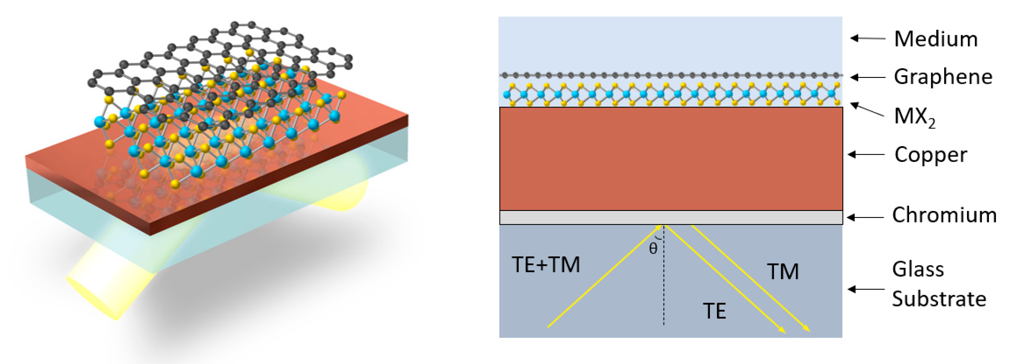
2. Methods
- Angle interrogation;
- Wavelength interrogation;
- Phase change measurements;
2.1. Reflectivity (Rp) and Phase (ϕp) Calculations
2.2. Goos-Hanchen (GH) Shift Calculations
3. Results
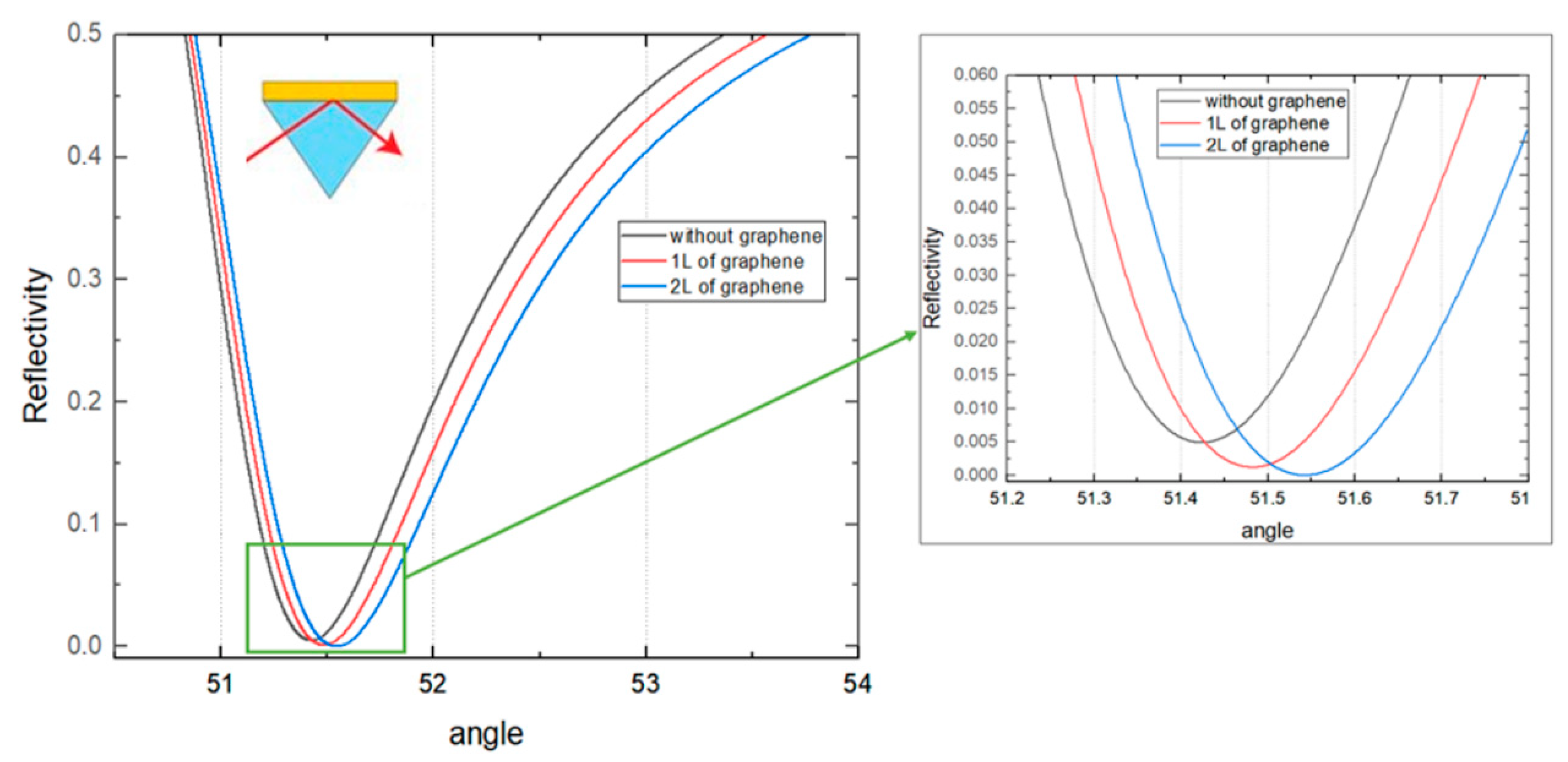
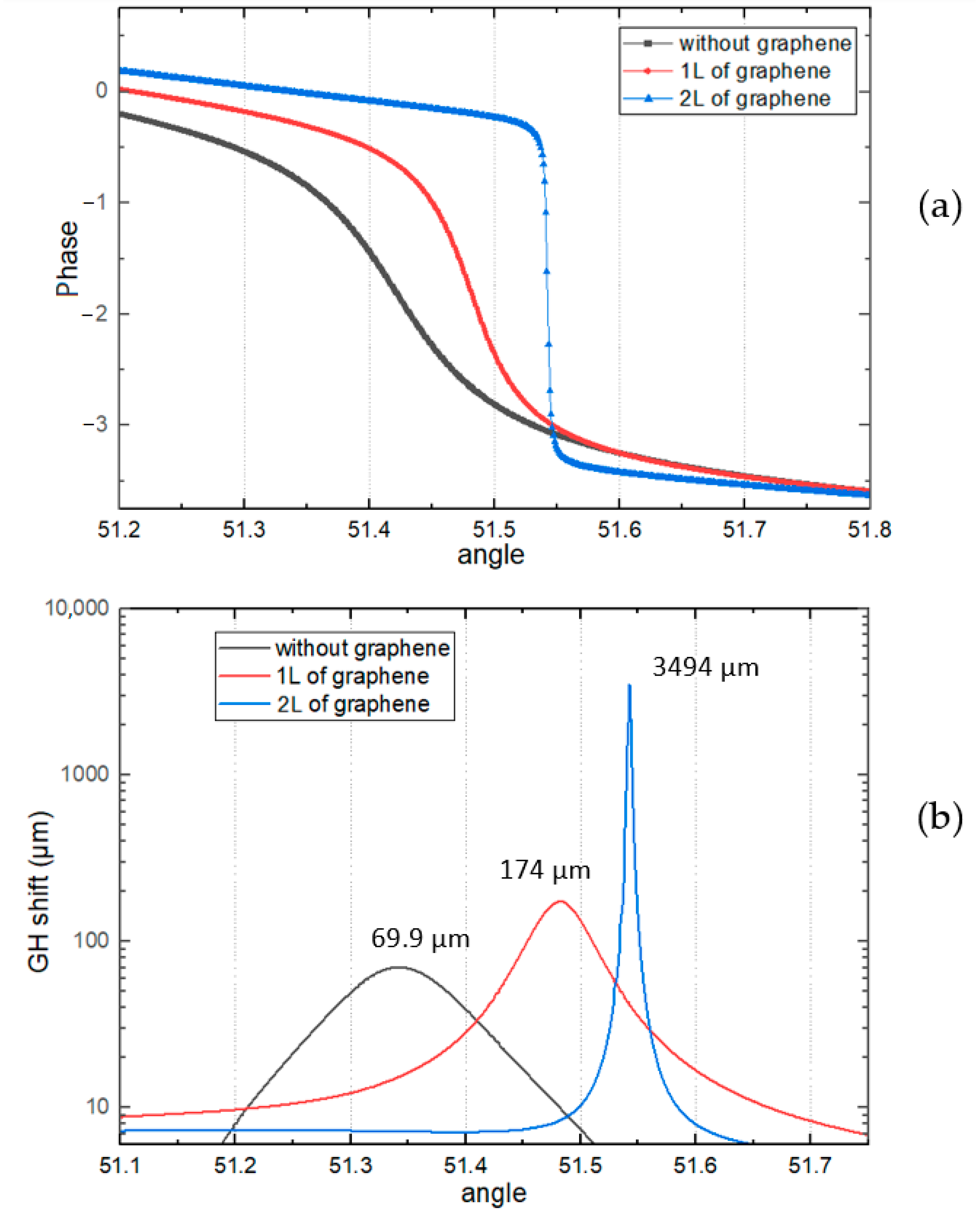
3.1. Reflectance, Phase Change and GH Shift of WSe2 Structure
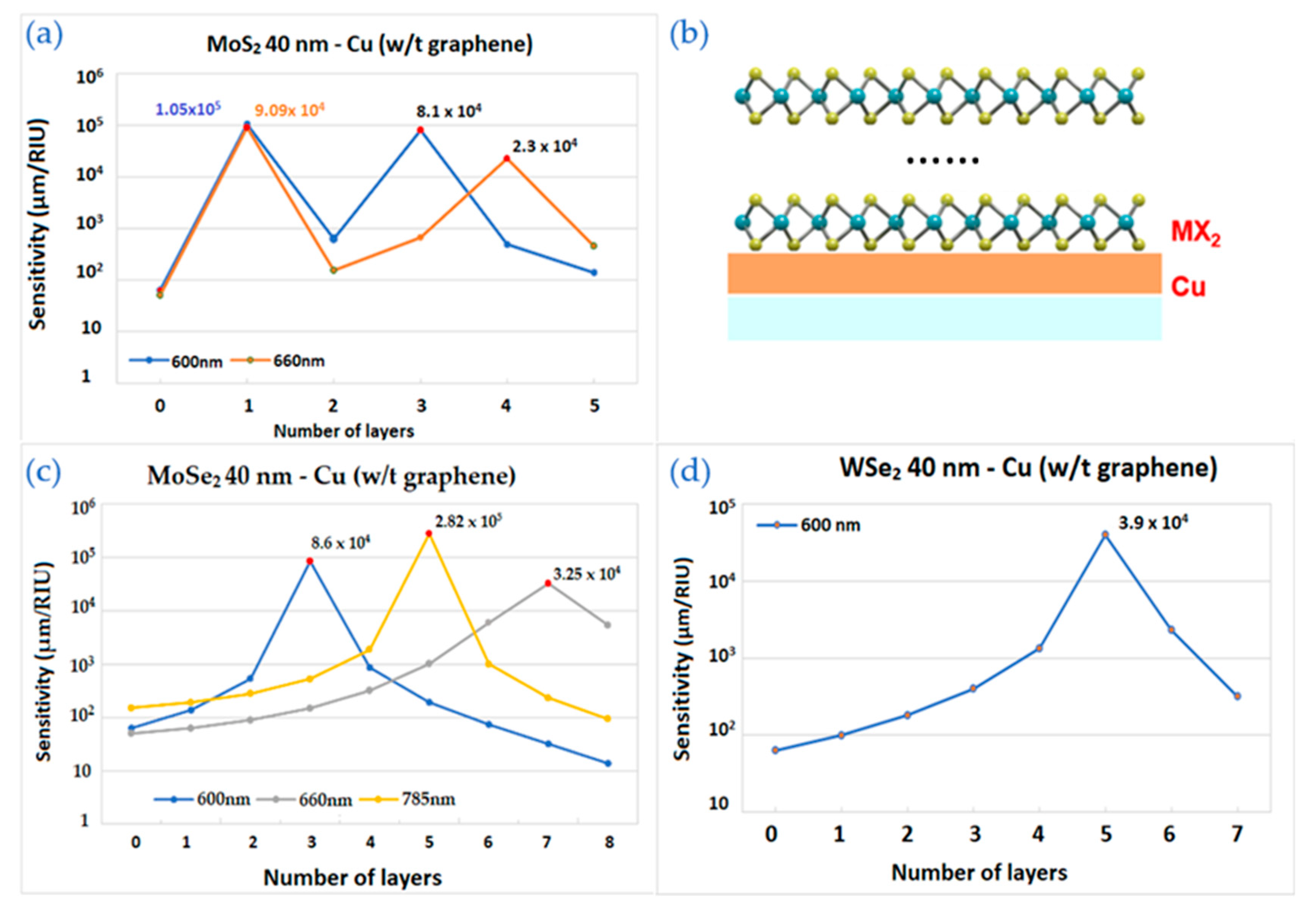
3.2. Sensitivity with Graphene Layers
3.3. Sensitivity with TMDC Enhanced Model
3.4. Sensitivity for TMDC and Graphene Enhanced Model
4. Discussion
4.1. Comparison of Structures without and 1, 2 Layers of Graphene
4.2. Best Results for Each Wavelength
5. Conclusions
Author Contributions
Funding
Data Availability Statement
Conflicts of Interest
Appendix A. Refractive Indices of Layers

| Type of TMDC | Thickness of Monolayer TMDC (nm) | λ = 600 nm | λ = 633 nm | λ = 660 nm | λ = 785 nm | λ = 1024 nm |
|---|---|---|---|---|---|---|
| MoS2 | 0.65 | n = 4.3934 | n = 5.0805 | n = 4.9991 | n = 4.6348 | n = 4.5660 |
| κ = 1.2269 | κ = 1.1723 | κ = 1.2563 | κ = 0.1163 | κ = 0.1058 | ||
| MoSe2 | 0.7 | n = 4.7586 | n = 4.6226 | n = 4.4963 | n = 4.2984 | n = 3.8768 |
| κ = 1.1504 | κ = 1.0063 | κ = 0.9382 | κ = 0.8225 | κ = 0.3561 | ||
| WS2 | 0.8 | n = 3.5202 | n = 4.8937 | n = 4.4735 | n = 4.0123 | n = 5.0110 |
| κ = 0.6048 | κ = 0.3124 | κ = 0.2059 | κ = 0.0399 | κ = 0.2562 | ||
| WSe2 | 0.7 | n = 4.5039 | n = 4.5501 | n = 4.3357 | n = 4.3655 | n = 4.8690 |
| κ = 0.9340 | κ = 0.4332 | κ = 0.2532 | κ = 0.0367 | κ = 0.2444 |
References
- Liedberg, B.; Nylander, C.; Lundström, I. Biosensing with surface plasmon resonance—How it all started. Biosens. Bioelectron. 1995, 10, 1–9. [Google Scholar] [CrossRef]
- Zheng, G.; Chen, Y.; Bu, L.; Xu, L.; Su, W. Waveguide-coupled surface phonon resonance sensors with super-resolution in the mid-infrared region. Opt. Lett. 2016, 41, 1582–1585. [Google Scholar] [CrossRef] [PubMed]
- Gupta, G.; Kondoh, J. Tuning and sensitivity enhancement of surface plasmon resonance sensor. Sens. Actuators B Chem. 2007, 122, 381–388. [Google Scholar] [CrossRef]
- Jia, B.; Chen, J.; Zhou, J.; Zeng, Y.; Ho, H.-P.; Shao, Y. Passively and actively enhanced surface plasmon resonance sensing strategies towards single molecular detection. Nano Res. 2022, 15, 8367–8388. [Google Scholar] [CrossRef]
- Naik, G.V.; Shalaev, V.M.; Boltasseva, A. Alternative Plasmonic Materials: Beyond Gold and Silver. Adv. Mater. 2013, 25, 3264–3294. [Google Scholar] [CrossRef] [PubMed]
- Futamata, M. Application of attenuated total reflection surface-plasmon-polariton Raman spectroscopy to gold and copper. Appl. Opt. 1997, 36, 364–375. [Google Scholar] [CrossRef] [PubMed]
- Kang, L.; Chu, J.; Zhao, H.; Xu, P.; Sun, M. Recent progress in the applications of graphene in surface-enhanced Raman scattering and plas-mon-induced catalytic reactions. J. Mater. Chem. C 2015, 3, 9024–9037. [Google Scholar] [CrossRef]
- Geim, A.K.; Novoselov, K.S. The rise of graphene. Nanosci. Technol. 2010, 1, 11–19. [Google Scholar]
- Xue, Y.; Wu, B.; Guo, Y.; Huang, L.; Jiang, L.; Chen, J.; Geng, D.; Liu, Y.; Hu, W.; Yu, G. Synthesis of large-area, few-layer graphene on iron foil by chemical vapor deposition. Nano Res. 2011, 4, 1208–1214. [Google Scholar] [CrossRef]
- Kravets, V.G.; Jalil, R.; Kim, Y.-J.; Ansell, D.; Aznakayeva, D.E.; Thackray, B.; Britnell, L.; Belle, B.D.; Withers, F.; Radko, I.; et al. Graphene-protected copper and silver plasmonics. Sci. Rep. 2014, 4, 5517. [Google Scholar] [CrossRef]
- Maurya, J.B.; Prajapati, Y.K. A comparative study of different metal and prism in the surface plasmon resonance bio-sensor having MoS2-graphene. Opt. Quantum Electron. 2016, 48, 1–12. [Google Scholar] [CrossRef]
- Wang, M.; Huo, Y.; Jiang, S.; Zhang, C.; Yang, C.; Ning, T.; Liu, X.; Li, C.; Zhang, W.; Man, B. Theoretical design of a surface plasmon resonance sensor with high sensitivity and high resolution based on graphene–WS2 hybrid nanostructures and Au–Ag bimetallic film. RSC Adv. 2017, 7, 47177–47182. [Google Scholar] [CrossRef]
- Passian, A.; Imam, N. Nanosystems, Edge Computing, and the Next Generation Computing Systems. Sensors 2019, 19, 4048. [Google Scholar] [CrossRef]
- Huamán, A.; Usaj, G. Anomalous Goos-Hänchen shift in the Floquet scattering of Dirac fermions. Phys. Rev. A 2019, 100, 033409. [Google Scholar] [CrossRef]
- Shaaban, A.; Hameed, M.F.O.; Gomaa, L.; Obayya, S. Accurate calculation of Goos-Hänchen shift at critical angle for complex laser beam profiles using beam propagation method. Optik 2018, 157, 1106–1114. [Google Scholar] [CrossRef]
- Yin, X.; Hesselink, L.; Liu, Z.; Fang, N.; Zhang, X. Large positive and negative lateral optical beam displacements due to surface plasmon resonance. Appl. Phys. Lett. 2004, 85, 372–374. [Google Scholar] [CrossRef]
- A Carvalho, S.; De Leo, S.; Huguenin, J.A.O.; Martino, M.; Da Silva, L. Experimental evidence of laser power oscillations induced by the relative Fresnel (Goos–Hänchen) phase. Laser Phys. Lett. 2019, 16, 065001. [Google Scholar] [CrossRef]
- Kravets, V.G.; Schedin, F.; Jalil, R.; Britnell, L.; Gorbachev, R.; Ansell, D.; Thackray, B.; Novoselov, K.; Geim, A.K.; Kabashin, A.; et al. Singular phase nano-optics in plasmonic metamaterials for label-free single-molecule detection. Nat. Mater. 2013, 12, 304–309. [Google Scholar] [CrossRef]
- Saito, H.; Neo, Y.; Matsumoto, T.; Tomita, M. Giant and highly reflective Goos-Hänchen shift in a metal-dielectric multilayer Fano structure. Opt. Express 2019, 27, 28629–28639. [Google Scholar] [CrossRef]
- Malik, A.; You-Lin, C.; Muqadder, A. Giant negative and positive Goos–Hänchen shifts via Doppler broadening effect. Laser Phys. 2019, 29, 075201. [Google Scholar] [CrossRef]
- Kooyman, R.P.H. Physics of Surface Plasmon Resonance. In Handbook of Surface Plasmon Resonance; Royal Society of Chemistry: London, UK, 2008. [Google Scholar]
- Kretschmann, E.; Raether, H. Notizen: Radiative Decay of Non Radiative Surface Plasmons Excited by Light. Z. Nat. A 1968, 23, 2135–2136. [Google Scholar] [CrossRef]
- Sreekanth, K.V.; Das, C.M.; Medwal, R.; Mishra, M.; Oyang, Q.; Rawat, R.S.; Yong, K.-T.; Sing, R. Electrically Tunable Singular Phase and Goos–Hänchen Shifts in Phase-Change-Material-Based Thin-Film Coatings as Optical Absorbers. Adv. Mater. 2021, 33, 2006926. [Google Scholar] [CrossRef] [PubMed]
- Zeng, S.; Hu, S.; Xia, J.; Anderson, T.; Dinh, X.-Q.; Meng, X.-M.; Coquet, P.; Yong, K.-T. Graphene–MoS2 hybrid nanostructures enhanced surface plasmon resonance biosensors. Sens. Actuators B Chem. 2015, 207, 801–810. [Google Scholar] [CrossRef]
- Zeng, S.; Baillargeat, D.; Ho, H.-P.; Yong, K.-T. Nanomaterials enhanced surface plasmon resonance for biological and chemical sensing applications. Chem. Soc. Rev. 2014, 43, 3426–3452. [Google Scholar] [CrossRef]
- Xiong, X.; Jiang, C.; Xie, Q. Broadband transmission properties of graphene-dielectric interfaces. Results Phys. 2019, 14, 102521. [Google Scholar] [CrossRef]
- Chaves, A.; Azadani, J.G.; Alsalman, H.; Da Costa, D.R.; Frisenda, R.; Chaves, A.J.; Song, S.H.; Kim, Y.D.; He, D.; Zhou, J.; et al. Bandgap engineering of two-dimensional semiconductor materials. NPJ 2D Mater. Appl. 2020, 4, 1–21. [Google Scholar] [CrossRef]
- Wu, L.; Chu, H.S.; Koh, W.S.; Li, E.P. Highly sensitive graphene biosensors based on surface plasmon resonance. Opt. Express 2010, 18, 14395–14400. [Google Scholar] [CrossRef]
- Zeng, Y.; Hu, R.; Wang, L.; Gu, D.; He, J.; Wu, S.-Y.; Ho, H.-P.; Li, X.; Qu, J.; Gao, B.Z.; et al. Recent advances in surface plasmon resonance imaging: Detection speed, sensitivity, and portability. Nanophotonics 2017, 6, 1017–1030. [Google Scholar] [CrossRef]
- Polyanskiy, M.N. Refractive Index Database. Available online: https://refractiveindex.info (accessed on 25 April 2022).
- Johnson, P.B.; Christy, R.W. Optical constants of transition metals: Ti, V, Cr, Mn, Fe, Co, Ni, and Pd. Phys. Rev. B 1974, 9, 5056. [Google Scholar] [CrossRef]
- Johnson, P.B.; Christy, R.W. Optical Constants of the Noble Metals. Phys. Rev. B 1972, 6, 4370. [Google Scholar] [CrossRef]
- Bruna, M.; Borini, S.M. Optical constants of graphene layers in the visible range. Appl. Phys. Lett. 2009, 94, 031901. [Google Scholar] [CrossRef]
- Li, Y.; Chernikov, A.; Zhang, X.; Rigosi, A.; Hill, H.M.; van der Zande, A.M.; Chenet, D.A.; Shih, E.-M.; Hone, J.; Heinz, T.F. Measurement of the optical dielectric function of monolayer transition-metal dichalcogenides: MoS2, MoSe2, WS2, and WSe2. Phys. Rev. B 2014, 90, 205422. [Google Scholar] [CrossRef]
- Liu, H.-L.; Shen, C.-C.; Su, S.-H.; Hsu, C.-L.; Li, M.-Y.; Li, L.-J. Optical properties of monolayer transition metal dichalcogenides probed by spectroscopic ellipsometry. Appl. Phys. Lett. 2014, 105, 201905. [Google Scholar] [CrossRef]
- Ouyang, Q.; Zeng, S.; Jiang, L.; Hong, L.; Xu, G.; Dinh, X.Q.; Qian, J.; He, S.; Qu, J.; Coquet, P.; et al. Sensitivity Enhancement of Transition Metal Dichalcogenides/Silicon Nanostructure-based Surface Plasmon Resonance Biosensor. Sci. Rep. 2016, 6, 28190. [Google Scholar] [CrossRef] [Green Version]


| Wavelength | ||||||
|---|---|---|---|---|---|---|
| Thickness of the Copper | 600 nm | 633 nm | 660 nm | 785 nm | 1024 nm | |
| Without graphene | 30 nm | 3.38 | 7.18 | 11.56 | 29.65 | 216.72 |
| 35 nm | 10.23 | 14.04 | 22.05 | 59.75 | 981.35 | |
| 40 nm | 63.10 | 34.84 | 50.18 | 150.10 | 4447.87 | |
| 45 nm | 277.06 | 174.17 | 193.18 | 1164.60 | 39.95 | |
| 50 nm | 11.36 | 678.01 | 6137.02 | 372.84 | 30.87 | |
| 2 layers of graphene | 30 nm | 3.34 | 6.82 | 11.17 | 30.01 | 270.72 |
| 35 nm | 11.57 | 15.04 | 23.93 | 67.40 | 3498.87 | |
| 40 nm | 115.72 | 46.42 | 68.06 | 237.52 | 315.04 | |
| 45 nm | 81.11 | 841.49 | 847.31 | 20,139.79 | 16.52 | |
| 50 nm | 7.39 | 73.74 | 129.85 | 38.17 | 29.42 | |
| Thickness of Copper | Without Graphene (µm/RIU) | With 1 Layer of Graphene (µm/RIU) | With 2 Layers of Graphene (µm/RIU) | |
|---|---|---|---|---|
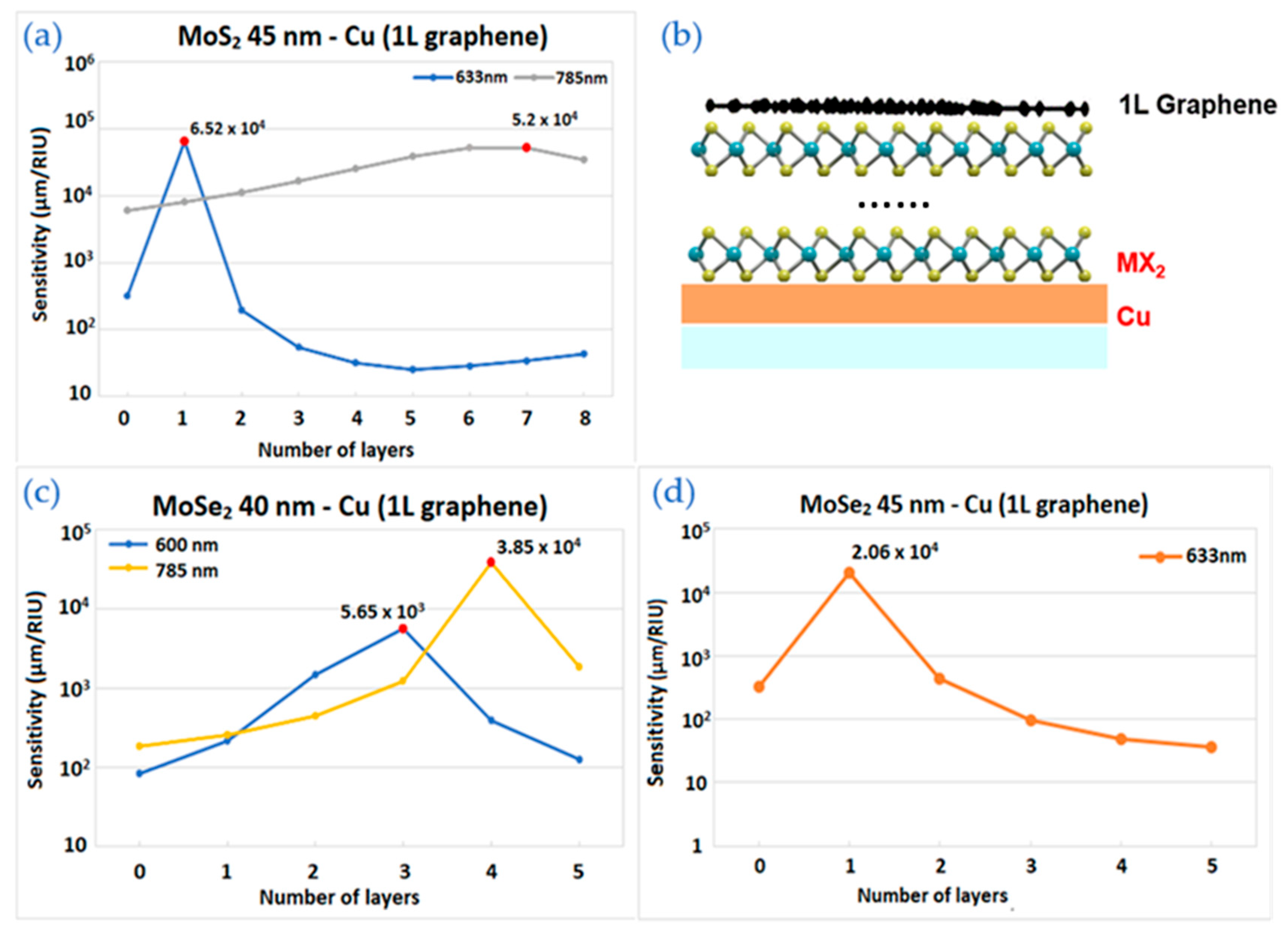
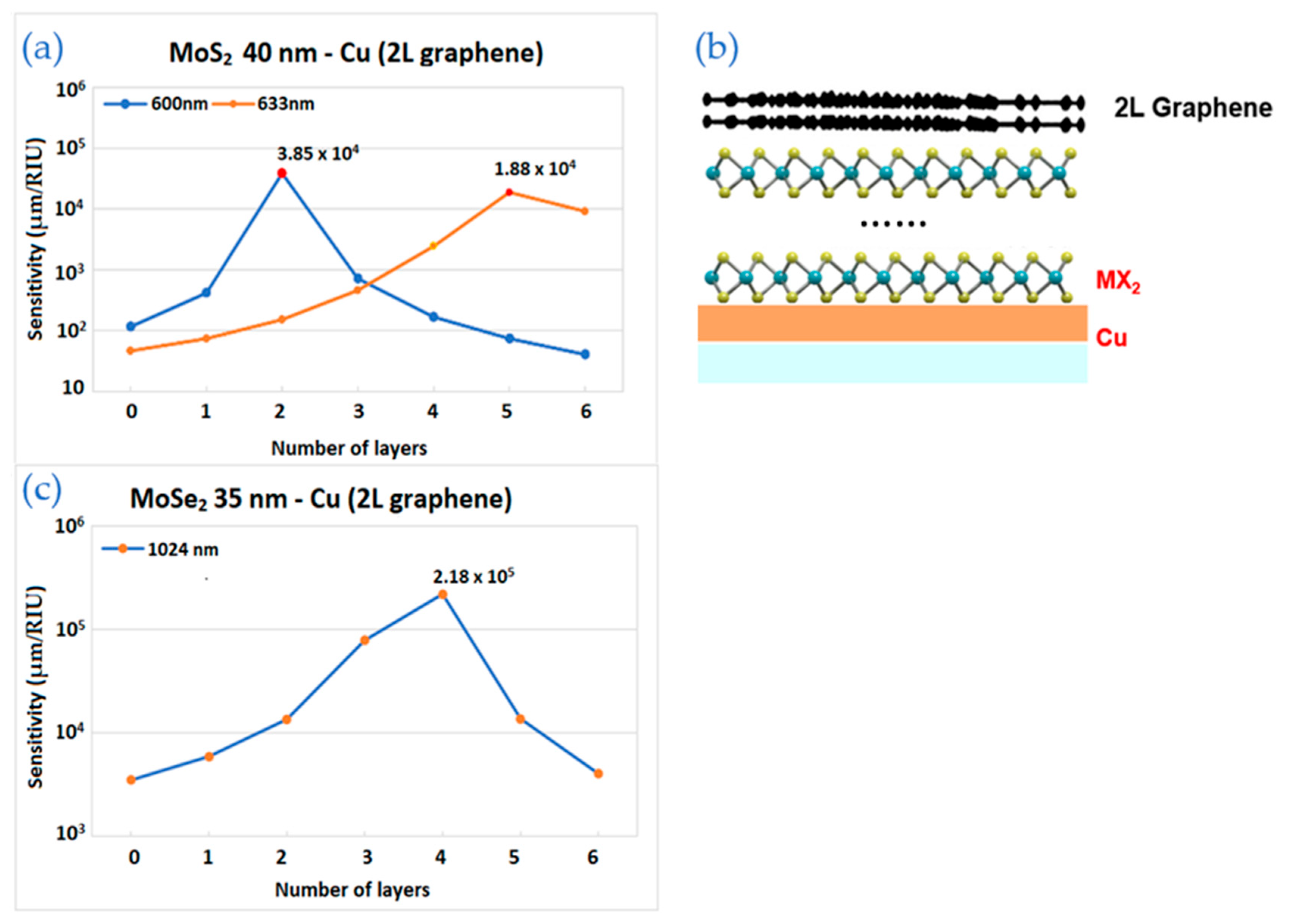
| MoS2 | 45 nm | 1.05 × 10⁵ (1 L, 600 nm) | 6.52 × 10⁴ (6 L, 633 nm) | 3.85 × 10⁴ (2 L, 600 nm) |
| MoSe2 | 35 nm | 2.46 × 10⁵ (8 L, 1024 nm) | 2.18 × 10⁵ (4 L, 1024 nm) | |
| 40 nm | 2.82 × 10⁵ (5 L, 785 nm) | 3.84 × 10⁴ (4 L, 785 nm) | 1.27 × 10⁴ (2 L, 600 nm) | |
| 45 nm | 2.89 × 10⁴ (1 L, 785 nm) | 2.06 × 10⁴ (1 L, 633 nm) | 8066 (1 L, 660 nm) | |
| WS2 | 40 nm | 4146 (10 L, 600 nm) | 5788 (9 L, 600 nm) | |
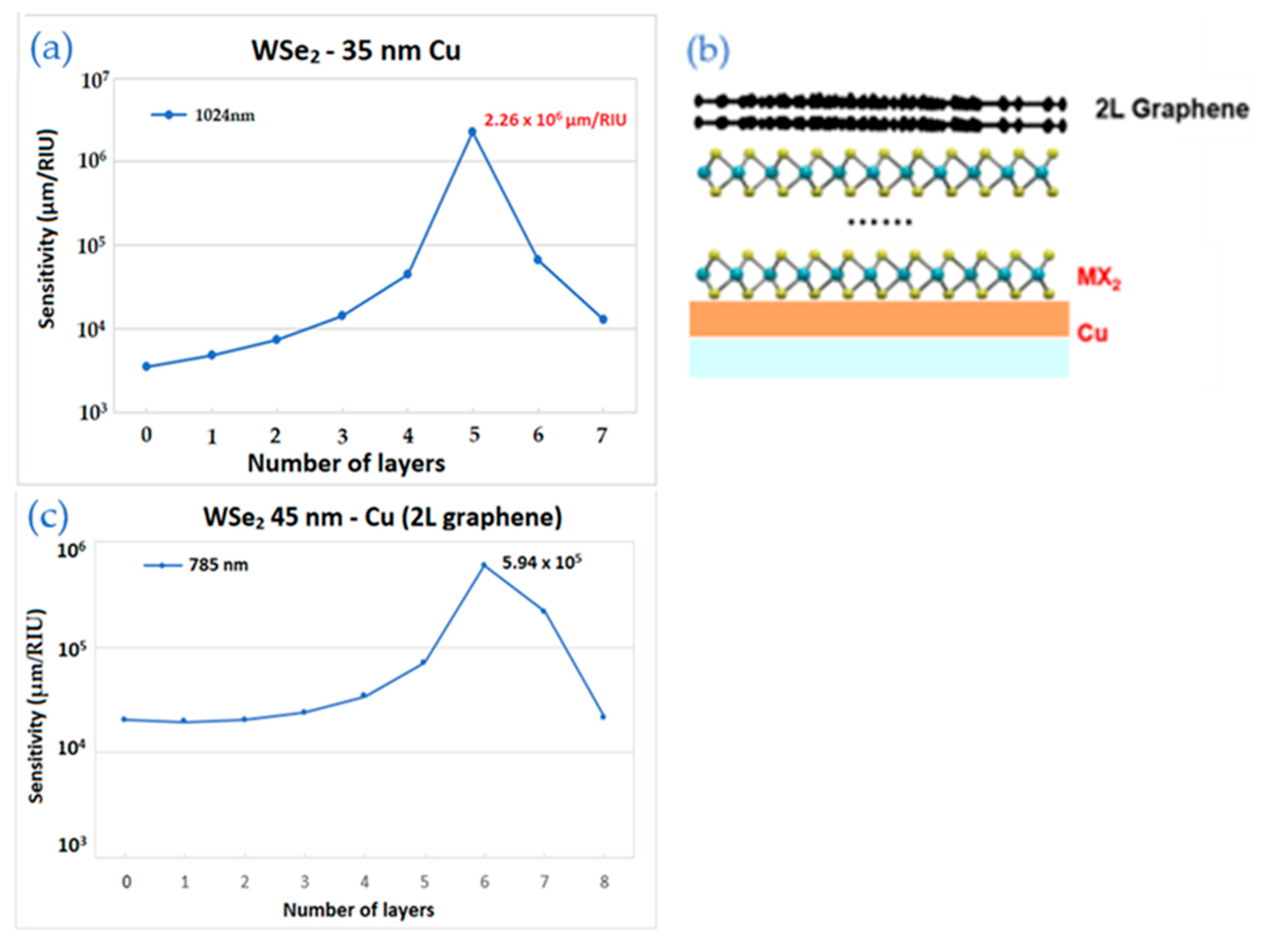
| WSe2 | 35 nm | 5155 (9 L, 1024 nm) | 3.17 × 10⁵ (9 L, 1024 nm) | 2.26 × 10⁶ (5 L, 1024 nm) |
| 40 nm | 3.99 × 10⁴ (5 L, 600 nm) | 1.03 × 10⁴ (4 L, 600 nm) | 1.66 × 10⁴ (4 L, 600 nm) | |
| 45 nm | 346 (3 L, 633 nm) | 1036 (3 L, 633 nm) | 5.94 × 10⁵ (6 L, 785 nm) |
| Excitation Wavelength (nm) | Thickness of Copper (nm) | Type of TMDC | Number of TMDC Layers | Number of Graphene Layers | Sensitivity (µm/RIU) |
|---|---|---|---|---|---|
| 600 | 40 | WSe2 | 5 | 0 | 3.99 × 10⁴ |
| 633 | 45 | MoSe2 | 1 | 1 | 2.06 × 10⁴ |
| 660 | 40 | MoS2 | 1 | 0 | 9.09 × 10⁴ |
| 785 | 40 | WSe2 | 6 | 2 | 5.94 × 10⁵ |
| 1024 | 35 | WSe2 | 5 | 2 | 2.26 × 10⁶ |
Publisher’s Note: MDPI stays neutral with regard to jurisdictional claims in published maps and institutional affiliations. |
© 2022 by the authors. Licensee MDPI, Basel, Switzerland. This article is an open access article distributed under the terms and conditions of the Creative Commons Attribution (CC BY) license (https://creativecommons.org/licenses/by/4.0/).
Share and Cite
Zakirov, N.; Zhu, S.; Bruyant, A.; Lérondel, G.; Bachelot, R.; Zeng, S. Sensitivity Enhancement of Hybrid Two-Dimensional Nanomaterials-Based Surface Plasmon Resonance Biosensor. Biosensors 2022, 12, 810. https://doi.org/10.3390/bios12100810
Zakirov N, Zhu S, Bruyant A, Lérondel G, Bachelot R, Zeng S. Sensitivity Enhancement of Hybrid Two-Dimensional Nanomaterials-Based Surface Plasmon Resonance Biosensor. Biosensors. 2022; 12(10):810. https://doi.org/10.3390/bios12100810
Chicago/Turabian StyleZakirov, Nurzad, Shaodi Zhu, Aurélien Bruyant, Gilles Lérondel, Renaud Bachelot, and Shuwen Zeng. 2022. "Sensitivity Enhancement of Hybrid Two-Dimensional Nanomaterials-Based Surface Plasmon Resonance Biosensor" Biosensors 12, no. 10: 810. https://doi.org/10.3390/bios12100810