1. Introduction
The ionic bonded amorphous oxide semiconductor (AOS) materials with a large optical bandgap were introduced for the applications of transparent electrode like indium tin oxide (ITO) or zinc oxide (ZnO) [
1]. Nowadays, AOS have been used in active matrix devices of thin film transistor (TFT). The conduction band of the AOS is related with the ns orbitals of heavy metals, such as indium (In), gallium (Ga) and zinc (Zn). Even when AOS is composed in an amorphous phase, electrons can easily transport through the ns orbitals because the ns orbitals of AOS are overlapped by large size metals and are less sensitive to the arrangement of atoms [
2]. The AOS TFT has many advantages compared with an amorphous silicon (Si) based TFT. It has high field-effect mobility (~10 cm
2/Vs) and very low leakage current (~10
−12 A/cm
2) and it can be very uniformly fabricated even on flexible substrates [
3]. Moreover, AOS can be applicable for transparent and flexible display devices because it has a high optical bandgap (>3 eV) and it can be made at low process temperature (~200 °C) [
4]. In spite of a short period of research and developments, it can be used in the manufacturing of commercial display products for active matrix organic light emitting diodes (AMOLED) [
5].
In a future display, various active components such as pixel devices, gate and source driver, logic devices and non-volatile memory (NVM) will be integrated on a display panel. The basic operating of NVM devices is to store charges in a dielectric layer; when charges are trapped or detrapped in the dielectric layer of an NVM transistor, the threshold voltage (
VTH) of the transistor can be altered between two states as programming and erasing states. Two representative types of NVM in recent studies are floating gate and charge trapping layer memories [
6,
7]. In the floating gate NVM, the charges injected from a channel region through a tunneling layer are stored in a floating gate. The charge trapping NVM consists of three important layers: tunneling, charge trapping and blocking layers, where the charges are injected from a channel through the thin tunneling layer (a dielectric layer near the channel) and stored in the charge trapping layer. The thickness and interface traps of the tunnel layer are critical because they directly affect the electric field in the tunnel layer, which determines the tunnel current. The charge trapping layer stores the charges in the traps of the layer; as many shallow or deep traps, as possible are favorable. The blocking layer near the gate should be thick enough to block charge transport to the gate region, and the thickness and the trap states of the blocking layer must be carefully designed because they can also affect the electric field in the tunnel layer.
The AOS based charge trapping NVMs have been researched in previous literature. Zhang et al. fabricated a novel multi-level NVM using an amorphous Indium-Gallium-Zinc-Oxide (a-IGZO) layer as both storage and channel layers at low temperatures [
8] but reported the programming/erasing (P/E) characteristics with such drawbacks as poor data retention, insufficient mobility (~2 cm
2/Vs), and high erasing voltage (−15 V). Bak et al. reported on a-IGZO NVMs using an IGZO channel and ZnO trap layers fabricated at a low process temperature of 200 °C [
9], which also exhibited high programming/erase voltages (20 V/−20 V), lower mobility (0.2 cm
2/Vs), hump in transfer curve, and poor data retention. Yin et al. reported on an NVM with a bottom gate n-type IGZO TFT structure [
10,
11] of IGZO (channel)/Al
2O
3 (tunneling layer)/IGZO (charge trapping layer)/Al
2O
3 (blocking layer)/Mo (bottom gate) layers; low
VTH of 0.7 V and high field-effect mobility of 10.3 cm
2/Vs are exhibited, but reliability characteristics were still so poor that the program/erase cycles and retention time were less than 10
3 times and 10
3 s, respectively. The IGZO and its interface were not optimized yet as a charge trapping layer so that the stored charges easily escaped.
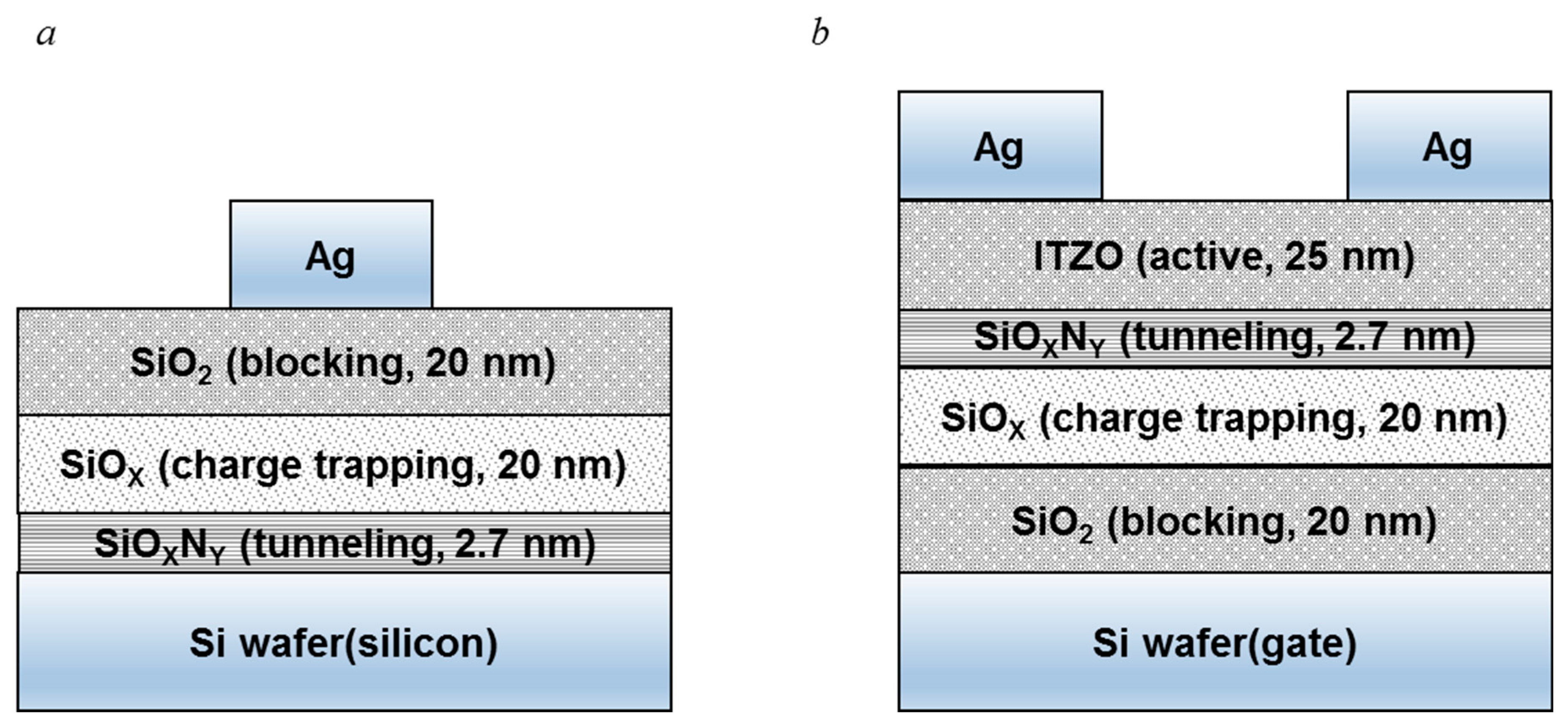
In this work, we fabricated a charge trapping NVM employing gallium free indium tin zinc oxide (ITZO) as an active channel layer of NVM and Si-rich oxide (SiO
X) as a charge trapping layer; the bottom gate ITZO NVM with SiO
2 (blocking layer)/SiO
X (charge trapping layer)/SiO
XN
Y (tunneling layer) was fabricated. The ITZO layer has many advantages in that it reported a high field-effect mobility (>30 cm
2/Vs) and high transparency [
12,
13]. The high field-effect mobility of the ITZO is useful for high density panels, such as virtual reality displays. Though the oxygen vacancies in the bulk and interface of the AOS channel might shift the
VTH under a bias voltage, these traps can be easily released by source-drain voltage, so that they will not influence on the long-term retention characteristics of NVM devices. The Si-rich SiO
X layer has many Si phases and defect sources in the SiO
X matrix, such as Si-H bonds in HSi
3O, HSi
2O
2, H
2SiO
2, so that it can enlarge memory windows, which means it has charge storage ability at a certain applied bias voltage. Moreover, the Si-rich SiO
X layer has low operating voltage, which can save the power consumption of a memory device. In addition, the charge states of the Si-rich SiO
X layer can be experimentally controlled or can be engineered and optimized by simply controlling a gas ratio of silane and nitrous oxide (SiH
4:N
2O) during the deposition process. Thus, the Si-rich SiO
X can be a very promising material as a charge trapping layer. The increase of states in the charge trapping layer was investigated by a fourier transform infrared (FT-IR) spectroscopy, and the expansion of the memory window was confirmed by capacitive-voltage (
C-V) measurement. The superior reliability characteristics of the fabricated bottom gate ITZO NVM was presented. This work will be useful to develop the next transparent future display integrating of display components.
3. Results & Discussions
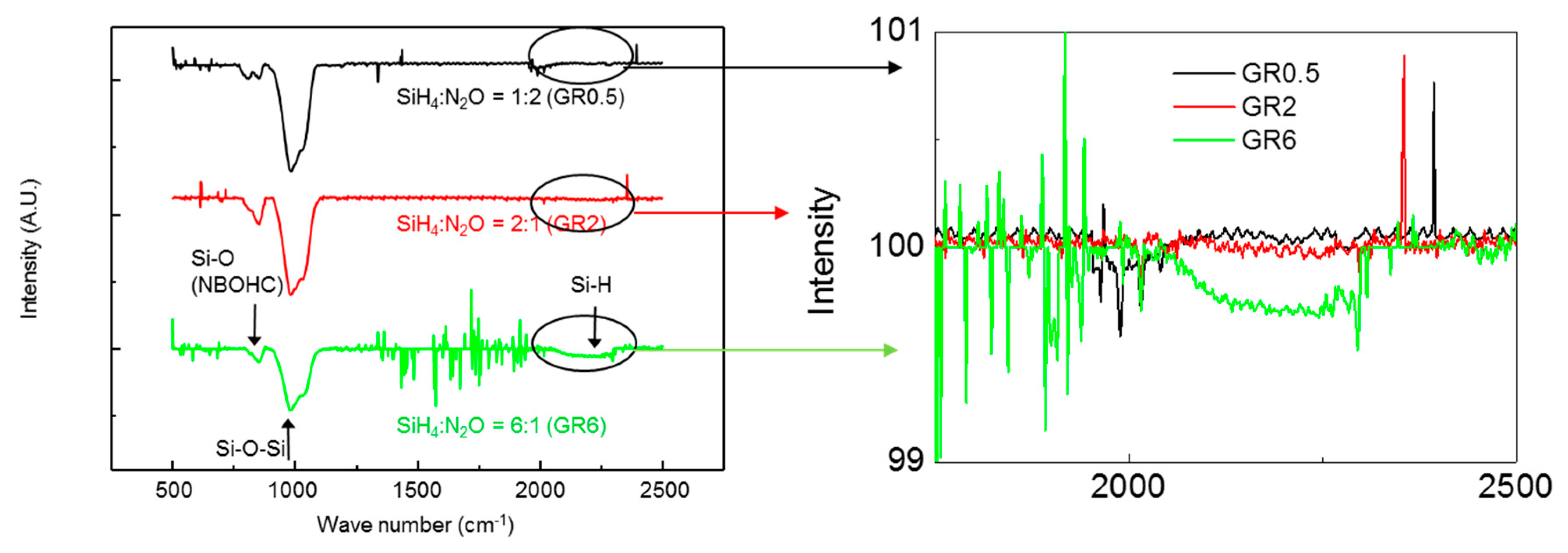
Figure 2 shows the measured results of FT-IR transmittance spectroscopy (Bruker, IFS-66/S) for the SiO
X charge trapping layer with a different SiH
4:N
2O gas ratio to evaluate as a charge trapping layer. The SiO
X layers showed the high absorption of Si-O bending peaks (or defects known as non-bridging oxygen hole center, NBOHC) at 860 cm
−1 [
15]. These NBOHC defects are known as the trapping sites to retain the injected charges. The charge trapping sites are observed in the all the conditions. In particular, SiO
x having a high Si content shows a remarkably large number of Si-H bonds as well as HSi
3O, HSi
2O
2, H
2SiO
2, and HSiO
3 at around 2000~2300 cm
−1 [
16,
17], and as the GR increases, the absorptions around 2000–2300 cm
−1 also increase. This implies that many Si phases and defects can exist in the Si-rich SiO
X. The numerous Si phases are desirable in a charge trapping layer because of their potential for large capacity and wide memory window, so the Si-rich SiO
X grown at the gas ratio of 6:1 is preferable.
The charging effects in conventional MIS structures are usually attributed to the traps in bulk of insulator and traps in the interface between the insulator and semiconductor. Each charge trapping effect can be distinguished by capacitance-voltage (C-V) measurement. To compare the charge storage characteristics of the NVMs for the charge storage layers grown by different SiH4:N2O GR conditions, the C-V characteristics of the MIS capacitors were measured at forward and reverse sweeping modes because each MIS capacitor has the same insulator structure of the NVM. In the case of the SiOX film using GR0.5, the charge trapping effect due to bulk trap in the insulator was high and the charge trapping effect due to the interface trap between insulator and semiconductor was almost zero.
Figure 3 shows measured
C-
V characteristics of the MIS capacitor with the insulator stack of SiO
2/SiO
X/SiO
XN
Y. A small voltage signal of 1 MHz was applied between top (Ag) electrode and bottom n-type single crystalline Si substrate with the bias voltage sweeping from depletion (−V) to accumulation (+V) for the capacitance measurement. At the positive bias voltage, electrons, the majority carriers of Si channel were accumulated at the interface to the SiO
XN
Y, the MIS capacitance was close to that of the overall insulator capacitor of SiO
2/SiO
X/SiO
XN
Y (C
OX, ~8.48 × 10
−8 F/cm
2). At the negative bias voltage, the electrons near the SiO
XN
Y were repelled and the depletion region was expanded until the inverted (p-type) channel was formed in the n-type Si region, so that the device capacitance becomes the effective value of series-connected capacitors made of the insulator capacitor, SiO
2/SiO
X/SiO
XN
Y and the depletion capacitor in the n-type Si substrate. When the bias voltage of the MIS capacitor was swept, the
C-
V characteristic curves were changed for the sweeping voltage range and the sweeping mode: forward (from negative to positive) and reverse (from positive to negative) mode. In the forward mode, part of the accumulated electrons at the interface to the SiO
XN
Y was trapped in the trapping layer via tunneling process, which kept the interface region of the n-type Si depleted even after the applied voltage was removed. In the reverse mode, the electrons in the trapping layer escaped to the n-type Si; the empty trap states (or holes occupied) induce the electrons in the n-type Si to reduce the depletion region. Therefore, the hysteresis curves are clockwise in
Figure 3.
The number of tunneled carriers depends both on the electric field intensity in the tunneling layer, and the amount of available states in the trapping layer. As the sweep voltage range increases from −5–5 V to −15–15 V, the flat band voltage (VFB) shifts due to electron or hole trappings also increasing. The flat band voltage at which population inversion occurred in the n-type Si (or channel) was determined by the metal-silicon work function difference and the various oxide charges. The total hysteresis can be presented the sum of the difference of the VFB shift (ΔVFB) by the hole and electron charging. Though the VFB of real MIS structures was further affected by the presence of charge in the oxide or at the oxide-semiconductor interface, for convenience, VFB was measured at middle of C-V curve in this paper.
When the charge trapping layer was deposited at the condition of GR0.5, the Δ
VFB was imperceptible even at the sweeping voltage of −15~15 V, and, the Δ
VFB from characteristic
C-
V curves was very small. It means that GR0.5 is not suitable for a charge trapping layer. When the charge trapping layer was deposited by GR2, Δ
VFB was 7.31 V in the large range voltage sweeps from −10 V to +10 V, but the Δ
VFB at the small sweep voltage range of −5–5 V is still imperceptible. This was attributed to small voltages not being able to give rise to a considerable charging effect in the defect sites of Si-rich SiO
X film. At the condition of GR6, wide Δ
VFB were exhibited as 10.92 and 2.47 V at the sweep voltage range of −10–10 and −5–5 V, respectively. As shown in
Figure 2, the charge trapping layer with more Si phases can increase the Δ
VFB (memory window) to more clearly distinguish memory states. The SiO
X layer grown at the highest SiH
4:N
2O gas ratio (GR6) condition can capture the greatest amount of charge with a large number of Si phases.
We compared the charge storage performance of the fabricated MIS capacitor for the GR condition of the charge trapping layer using the measured
C-
V characteristics.
Figure 4a,b shows the operation voltage of programming/erasing as a function of the bias voltage comparing GR2 and GR6. In both conditions, the Δ
VFB also increased with the applied bias voltage; the internal electrical field in the MIS capacitor increased with the bias voltage, which could facilitate the tunneling of the electrons, and make the electrons easily trapped or detrapped in the charge trapping layer. But, the difference of Δ
VFB was observed. At the bias voltage of ±11 V, the Δ
VFB were 2.18 and 4.45 V for the charge trapping layers of GR2 and GR6. The difference of Δ
VFB was due to the difference of charge trapping density as shown in FT-IR spectroscopy in
Figure 2; a higher trap density in the Si-rich SiO
X film can be obtained by the deposition under higher GR.
Figure 4c,d shows charge retention characteristics for the MIS capacitors of the different GR, which is induced from the
C-
V measurements. After applying the bias voltages of programming (11 V) and erasing (−11 V) to the MIS capacitors for 10 s,
C-
V characteristics were measured over time to extract Δ
VFB between the programming and erasing states. The initial Δ
VFB were 3.07 and 4.24 V for GR2 and GR6 MIS capacitors. The Δ
VFB was gradually degraded during the observation for 10
3 s. Assuming the same Δ
VFB deterioration trend, Δ
VFB was estimated to hold ~67% and ~71% of the initial Δ
VFB of GR2 and GR6 MIS capacitor for 10
9 s (nearly 10 years). Assuming that the NVM device was working 10 years, the retention of GR2 and GR6 was about 67% and 71% of each initial Δ
VFB, respectively. Additionally, a low operation voltage of about ±11 V was used. These good retention properties are promising for NVM because of using the SiO
2/SiO
X/SiO
XN
Y memory stack.
Figure 5 shows the drain current to gate voltage (
ID-
VGS) transfer characteristics of the fabricated metal/SiO
2/SiO
X/SiO
XN
Y/ITZO NVMs at programming and erasing modes, which is measured at the drain voltage of 1 V. The fabricated device exhibited excellent transistor characteristics because of the high field-effect mobility (
μFE) of ITZO layer. The measured initial values of
μFE,
VTH, subthreshold swing (S.S.), and on/off current ratio were 27.2 cm
2/Vs, 0.15 V, 0.17 V/dec and 7.57 × 10
7, respectively. At the program mode of the NVMs, the positive-voltage pulses of 1 μs in the voltage range of 9–13 V were applied to the gate, and the
ID-
VG transfer curves were shifted to the positive. When the positive voltage pulse was applied to the gate, an internal electric field was applied to the SiO
2/SiO
X/SiO
XN
Y dielectric stack. As a result, electrons could be injected from the conduction band of the ITZO channel through the tunneling layer and stored in the Si-rich SiO
X charge trapping sites. It is known that the electrons were trapped not only in shallow or deep traps of SiO
X, but also in OH¯, H
+ residues, and oxygen vacancy (V
O) sites at the interfaces with the ITZO channel layer in the programming mode [
18]. Thus, the memory window can be expected to increase due to the plenty of the negative charges. The Δ
VTH by the gate voltage pulses of 11 and 13 V were 2 and 3.7 V, respectively. Higher programing voltage and more states both in shallow or deep traps of the charge trapping layers add more advantages to the NVMs because the tunneling electric field can be higher with the gate voltage, and more electrons can be stored in the trap states as in the MIS capacitors.
Various tunneling mechanisms have been suggested, such as direct tunneling, Fowler–Nordheim (FN) tunneling and channel hot electron (CHE) tunneling processes [
19]. In our work, an ultra-thin tunneling layer of less than 4 nm was used, and the energy barrier (
ΦB) between ITZO and SiO
XN
Y was ~2 eV, so we expected that a direct tunneling process could be dominantly involved. We noted that specifying one of these processes was difficult because these processes can occur together. So, it can be done in future studies.
A transparent NVM can be programmed with the positive-voltage pulses at the gate with plentiful negative charges sources but erasing at the negative-voltage pulses at the gate cannot easily erase the NVMs. Even with the significant negative gate voltage (−20 V), the Δ
VTH did not move back to the negative direction, which was a very different result from the MIS capacitor. The erasing behavior in the AOS NVM was introduced [
20]. In the MIS on n-type Si substrate, the bandgap of Si was smaller than that of the Si-rich SiOx (~2.4 eV), so the trapped electrons could be easily tunneled to the conduction band of the n-type Si when the negative bias voltage bends the conduction band down. However, the bandgap of ITZO (~3.2 eV) was higher than that of Si-rich SiOx, and electrons could not tunnel to the inner state of the forbidden band (in the bandgap) of the ITZO channel at a low negative bias voltage. A possible reason for this result is that the AOS, such as IGZO and ITZO, has only an electron carrier in nature. When the negative voltage was applied in Si for the erasing operation, hole carriers were injected to the charge trapping layer through the tunneling layer. Then, injected electrons could be neutralized by the hole carrier. However, few hole carriers were available in erasing behavior. Thus, the
VTH in ITZO NVM was very difficult to shift back to the negative side.
As shown in
Figure 6, the injected electrons were detrapped from the programmed electrons using white light having a wavelength from 400 to 700 nm with 10 mWcm
−2 and negative gate bias of −1 V for 1 s. As a result, the transfer curve returned to the pristine value. It was also reported that there was charge detrapping behavior under the light-assisted erasing process [
21]. To investigate light induced erasing behavior, the optical bandgap was measured by UV-visible spectra. The optical bandgap of ITZO and SiO
XN
Y, SiO
X, was 3.05~3.15 eV, 5.1 eV and 2.3 eV, respectively. To explain erasing behavior,
Figure 6 shows a band diagram of the Metal/SiO
2/SiO
X/SiO
XN
Y/ITZO NVM under white light irradiation. When the white light was irradiated on the ITZO layer, the electron hole pair was generated. The negative gate voltage made the electric field so that holes were injected to the charge storage layer through the tunneling layer at the valance band of ITZO.
Because the low bandgap of the Si-rich SiO
X and very thin tunneling layer was used, it was expected that its low valence band offset was aligned with ITZO layer [
22,
23]. Thus, generated holes were easily trapped under light illumination at the SiO
X/SiO
XN
Y interface or at SiO
X bulk trap states in the storage layer. Injected holes were recombined with trapped electrons, and neutralized. Thus,
VTH in the fabricated NVM could return to the pristine value. Surplus electrons by white light in ITZO became carriers, so that carrier concentration as well as conductivity of ITZO layer was increased (
σ = qμn). It can move
VTH shift to negative direction like as a negative bias illumination stress (NBIS) condition [
24].
We need to note that the control of external light illumination must be considered to use the ITZO NVM devices properly. For the application of transparent NVM, in-depth research of erasing electrons will be required, such as integration with light emission devices, which can trigger the erasing operation. A bandgap engineering for the layer structure, optimizing the conduction/valance band offset between the tunneling layer and the charge trapping layer, can reduce tunnel barrier and improve the erasing operation, or the excitations of the trapped charges which can be done by local thermal heating or electro-magnetic resonating terminals can promote the tunneling process without the external light source.
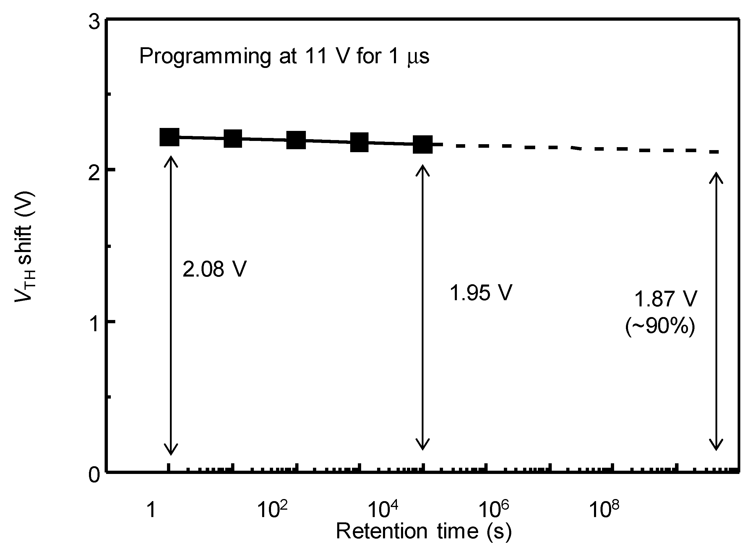
The retention characteristics of the fabricated Metal/SiO
2/SiO
X/SiO
XN
Y/ITZO NVM at programming state are shown in
Figure 7. After applying programming voltage pulse of 11 V and 1 μs, the threshold voltage shift was measured for 10
4 s. From the results of
Figure 7, it is expected that the shifted threshold voltage can be maintained for 10 years. The initial memory window was ~2.08 V, and after 10
4 s, the memory window was maintained as ~1.95 V and was expected to be ~1.87 V after 10 years; ~90% of the trapped charges can be retained for ~10 years.


