
Multi-Parametric Birefringence Control in Ultrashort-Pulse Laser-Inscribed Nanolattices in Fluorite
 , , , , , , and
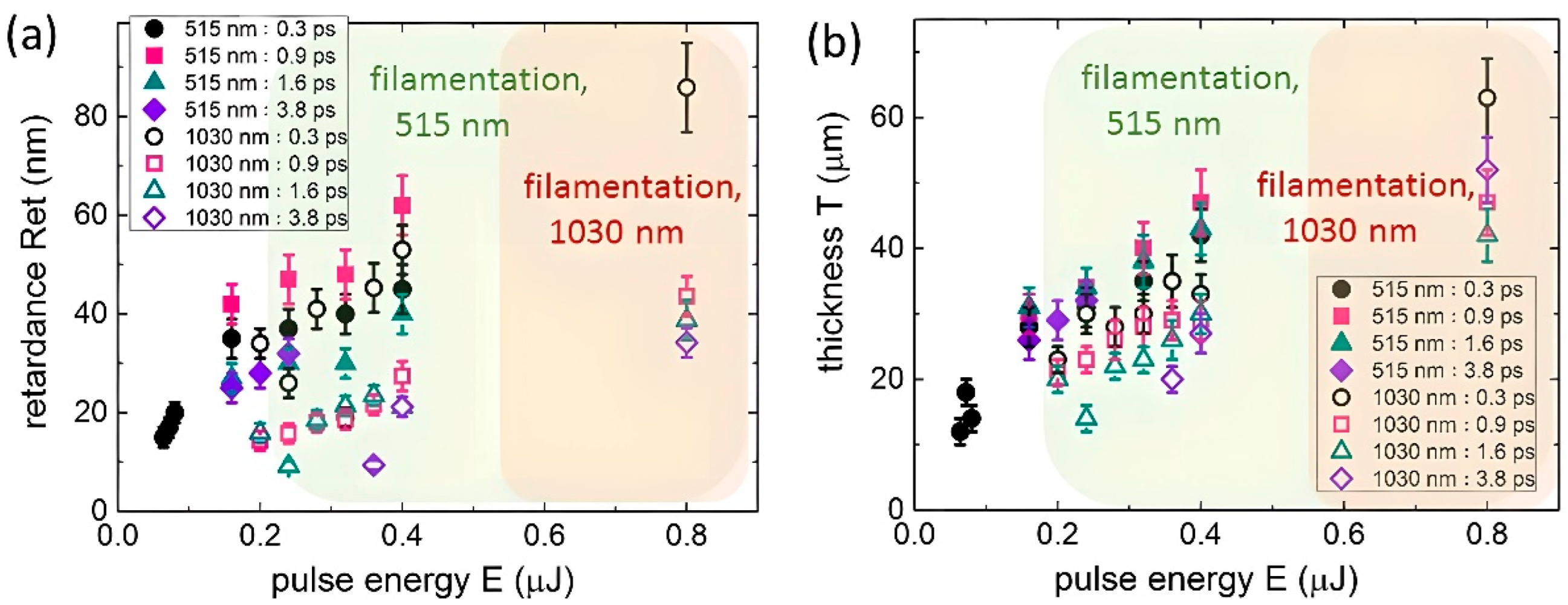
Abstract
:1. Introduction
2. Materials and Methods
3. Results and Discussion
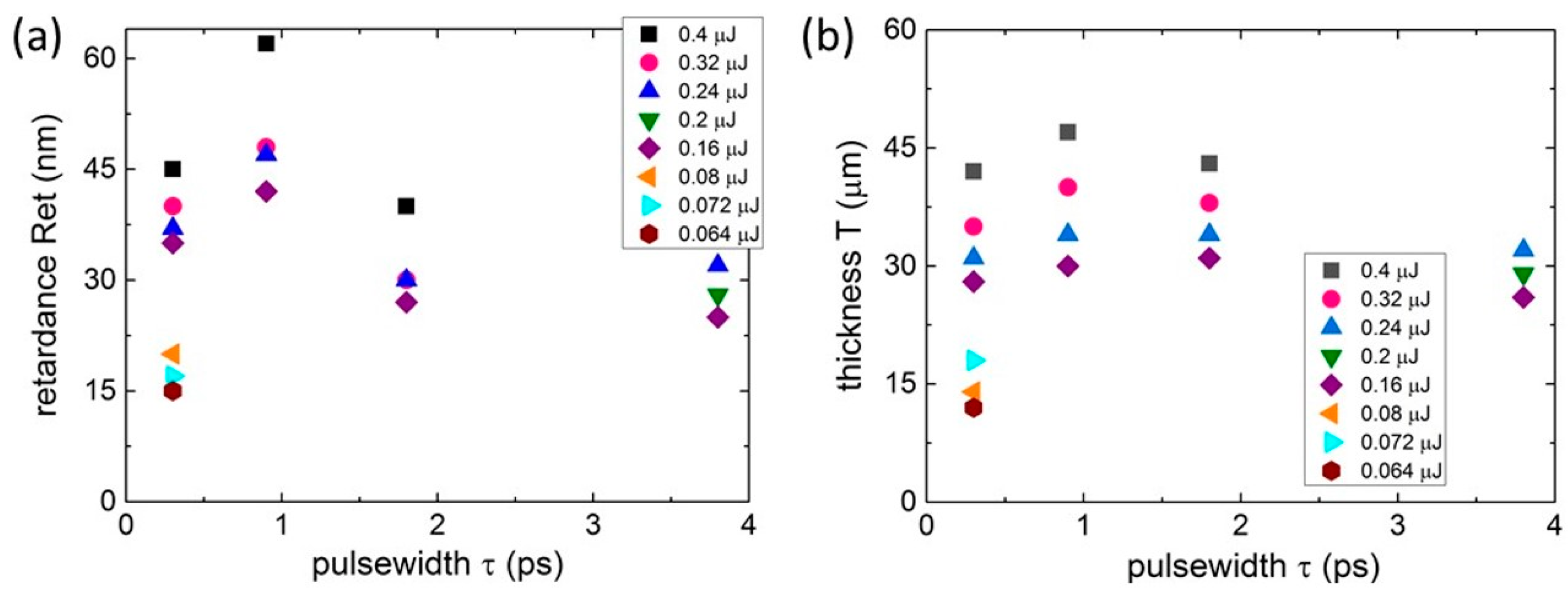
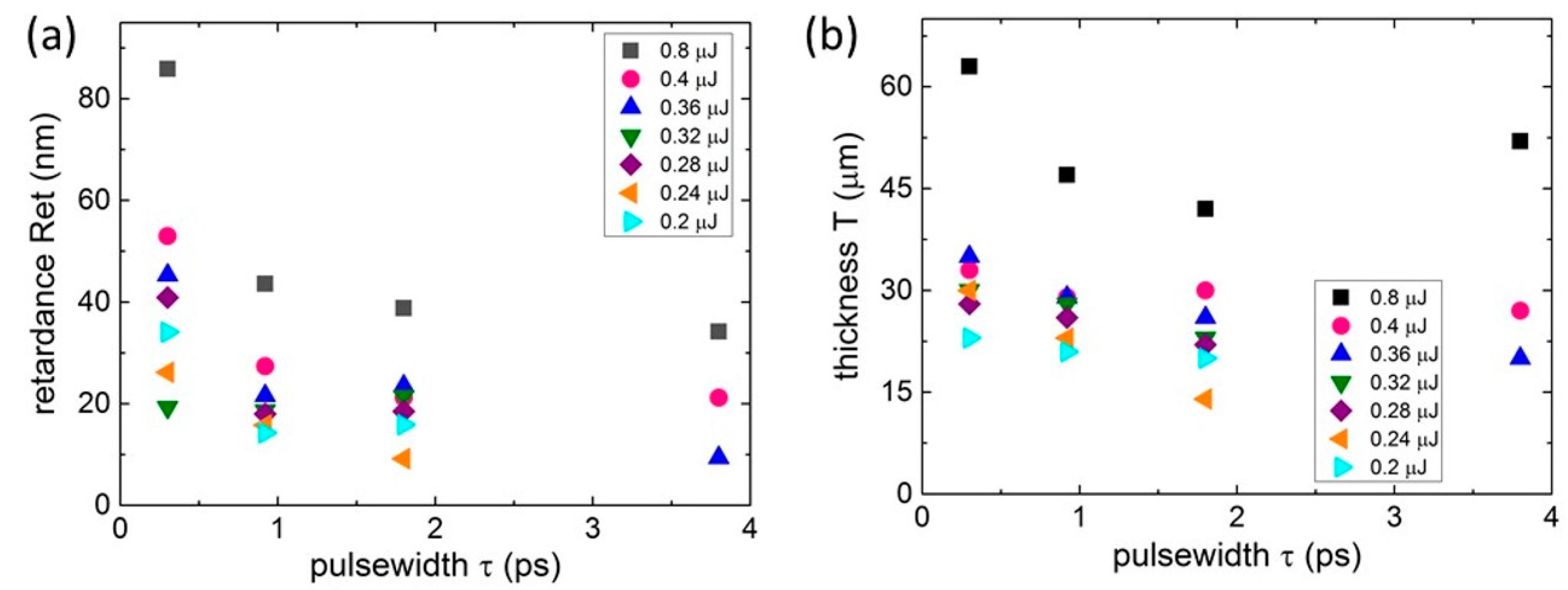
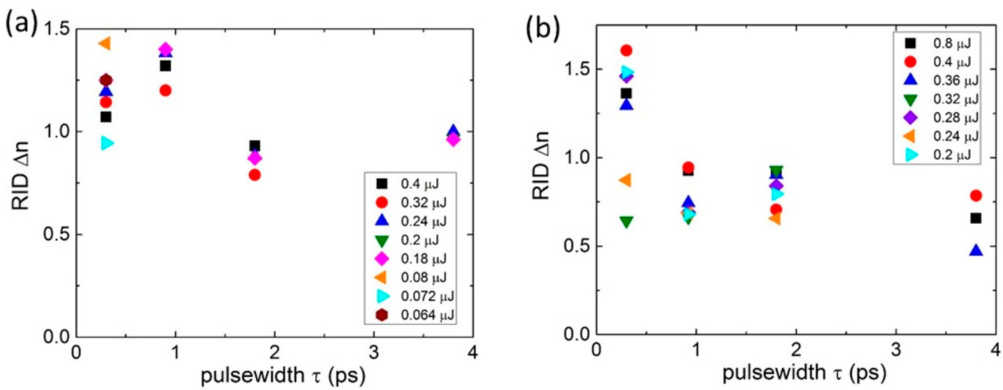
3.1. Characterization of Birefringent Nanolattices
3.2. Chemical Characterization of Inscribed Regions
3.3. Far-Field Optical Diffraction In Situ Characterization of Instantaneous Plasma and Accumulative Structural Changes
4. Conclusions
Supplementary Materials
Author Contributions
Funding
Data Availability Statement
Conflicts of Interest
References
- Shimotsuma, Y.; Kazansky, P.G.; Qiu, J.; Hirao, K. Self-Organized Nanogratings in Glass Irradiated by Ultrashort Light Pulses. Phys. Rev. Lett. 2003, 91, 247405. [Google Scholar] [CrossRef] [Green Version]
- Sakakura, M.; Lei, Y.; Wang, L.; Yu, Y.-H.; Kazansky, P.G. Ultralow-loss geometric phase and polarization shaping by ultrafast laser writing in silica glass. Light. Sci. Appl. 2020, 9, 15. [Google Scholar] [CrossRef] [PubMed] [Green Version]
- Xu, S.; Fan, H.; Li, Z.-Z.; Hua, J.-G.; Yu, Y.-H.; Wang, L.; Chen, Q.-D.; Sun, H.-B. Ultrafast laser-inscribed nanogratings in sapphire for geometric phase elements. Opt. Lett. 2021, 46, 536–539. [Google Scholar] [CrossRef] [PubMed]
- Rudenko, A.; Colombier, J.-P.; Höhm, S.; Rosenfeld, A.; Krüger, J.; Bonse, J.; Itina, T.E. Spontaneous periodic ordering on the surface and in the bulk of dielectrics irradiated by ultrafast laser: A shared electromagnetic origin. Sci. Rep. 2017, 7, 12306. [Google Scholar] [CrossRef] [PubMed] [Green Version]
- Taylor, R.; Hnatovsky, C.; Simova, E. Applications of femtosecond laser induced self-organized planar nanocracks inside fused silica glass. Laser Photon. Rev. 2008, 2, 26–46. [Google Scholar] [CrossRef]
- Zhang, B.; Liu, X.; Qiu, J. Single femtosecond laser beam induced nanogratings in transparent media—Mechanisms and ap-plications. J. Mater. 2019, 5, 1–14. [Google Scholar]
- Hnatovsky, C.; Taylor, R.S.; Rajeev, P.P.; Simova, E.; Bhardwaj, V.R.; Rayner, D.M.; Corkum, P.B. Pulse duration de-pendence of femtosecond-laser-fabricated nanogratings in fused silica. Appl. Phys. Lett. 2005, 87, 014104. [Google Scholar] [CrossRef]
- Beresna, M.; Gecevičius, M.; Kazansky, P.G. Ultrafast laser direct writing and nanostructuring in transparent materi-als. Adv. Opt. Photonics 2014, 6, 293–339. [Google Scholar] [CrossRef]
- Zimmermann, F.; Plech, A.; Richter, S.; Tünnermann, A.; Nolte, S. Ultrashort laser pulse induced nanogratings in borosilicate glass. Appl. Phys. Lett. 2014, 104, 211107. [Google Scholar] [CrossRef]
- Kudryashov, S.; Rupasov, A.; Zakoldaev, R.; Smaev, M.; Kuchmizhak, A.; Zolot’ko, A.; Kosobokov, M.; Akhmatkhanov, A.; Shur, V. Nanohydrodynamic Local Compaction and Nanoplasmonic Form-Birefringence Inscription by Ultrashort Laser Pulses in Nanoporous Fused Silica. Nanomaterials 2022, 12, 3613. [Google Scholar] [CrossRef]
- Kudryashov, S.; Rupasov, A.; Kosobokov, M.; Akhmatkhanov, A.; Krasin, G.; Danilov, P.; Lisjikh, B.; Abramov, A.; Greshnyakov, C.; Kuzmin, E.; et al. Hierarchical Multi-Scale Coupled Periodical Photonic and Plasmonic Nanopatterns Inscribed by Femtosecond Laser Pulses in Lithium Niobate. Nanomaterials 2022, 12, 4303. [Google Scholar] [CrossRef]
- Mizeikis, V.; Juodkazis, S.; Balciunas, T.; Misawa, H.; Kudryashov, S.I.; Ionin, A.A.; Zvorykin, V.D. Optical and ultrasonic signatures of femtosecond laser filamentation in fused silica. J. Appl. Phys. 2009, 105, 123106. [Google Scholar] [CrossRef]
- Schaffer, C.B.; Jamison, A.O.; Mazur, E. Morphology of femtosecond laser-induced structural changes in bulk transparent materials. Appl. Phys. Lett. 2004, 84, 1441–1443. [Google Scholar] [CrossRef] [Green Version]
- Kudryashov, S.I.; Danilov, P.A.; Rupasov, A.E.; Smayev, M.P.; Kirichenko, A.N.; Smirnov, N.A.; Ionin, A.A.; Zolot’Ko, A.S.; Zakoldaev, R.A. Birefringent microstructures in bulk fluorite produced by ultrafast pulsewidth-dependent laser inscription. Appl. Surf. Sci. 2021, 568, 150877. [Google Scholar] [CrossRef]
- Desmarchelier, R.; Poumellec, B.; Brisset, F.; Mazerat, S.; Lancry, M. In the Heart of Femtosecond Laser Induced Nanogratings: From Porous Nanoplanes to Form Birefringence. World J. Nano Sci. Eng. 2015, 5, 115–125. [Google Scholar] [CrossRef] [Green Version]
- Groothoff, N.; Hongler, M.-O.; Kazansky, P.; Bellouard, Y. Transition and self-healing process between chaotic and self-organized patterns observed during femtosecond laser writing. Opt. Express 2015, 23, 16993–17007. [Google Scholar] [CrossRef]
- Kudryashov, S.; Rupasov, A.; Kosobokov, M.; Akhmatkhanov, A.; Krasin, G.; Danilov, P.; Lisjikh, B.; Turygin, A.; Greshnyakov, E.; Kovalev, M.; et al. Ferroelectric Nanodomain Engineering in Bulk Lithium Niobate Crystals in Ultrashort-Pulse Laser Nanopatterning Regime. Nanomaterials 2022, 12, 4147. [Google Scholar] [CrossRef]
- Hayes, W.; Stoneham, A.M. Defects and Defect Processes in Nonmetallic Solids; Dover: New York, NY, USA, 1985. [Google Scholar]
- Kudryashov, S.; Danilov, P.; Smirnov, N.; Krasin, G.; Khmelnitskii, R.; Kovalchuk, O.; Kriulina, G.; Martovitskiy, V.; Lednev, V.; Sdvizhenskii, P.; et al. “Stealth Scripts”: Ultrashort Pulse Laser Luminescent Microscale Encoding of Bulk Diamonds via Ultrafast Multi-Scale Atomistic Structural Transformations. Nanomaterials 2023, 13, 192. [Google Scholar] [CrossRef]
- Kudryashov, S.I.; Danilov, P.A.; Kuzmin, E.V.; Gulina, Y.S.; Rupasov, A.E.; Krasin, G.K.; Zubarev, I.G.; Levchenko, A.O.; Kovalev, M.S.; Pakholchuk, P.P.; et al. Pulse-width-dependent critical power for self-focusing of ultrashort laser pulses in bulk dielectrics. Opt. Lett. 2022, 47, 3487–3490. [Google Scholar] [CrossRef]
- Danilov, P.; Kuzmin, E.; Rimskaya, E.; Chen, J.; Khmelnitskii, R.; Kirichenko, A.; Rodionov, N.; Kudryashov, S. Up/Down-Scaling Pho-toluminescent Micromarks Written in Diamond by Ultrashort Laser Pulses: Optical Photoluminescent and Structural Raman Imaging. Micromachines 2022, 13, 1883. [Google Scholar] [CrossRef]
- Mehta, S.B.; Shribak, M.; Oldenbourg, R. Polarized light imaging of birefringence and diattenuation at high resolution and high sensitivity. J. Opt. 2013, 15, 094007. [Google Scholar] [CrossRef] [PubMed] [Green Version]
- Kudryashov, S.I.; Nastulyavichus, A.A.; Saraeva, I.N.; Rudenko, A.A.; Zayarny, D.A.; Ionin, A.A. Deeply sub-wavelength laser nanopatterning of Si surface in dielectric fluids: Manipulation by surface plasmon resonance. Appl. Surf. Sci. 2020, 519, 146204. [Google Scholar] [CrossRef]
- Li, X.; Xu, J.; Lin, Z.; Qi, J.; Wang, P.; Chu, W.; Fang, Z.; Wang, Z.; Chai, Z.; Cheng, Y. Polarization-insensitive space-selective etching in fused silica induced by picosecond laser irradiation. Appl. Surf. Sci. 2019, 485, 188–193. [Google Scholar] [CrossRef] [Green Version]
- Smirnov, N.; Kudryashov, S.; Rudenko, A.; Zayarny, D.; Ionin, A. Pulsewidth and ambient medium effects during ultrashort-pulse laser ablation of silicon in air and water. Appl. Surf. Sci. 2021, 562, 150243. [Google Scholar] [CrossRef]
- Kudryashov, S.I. Some effects affecting laser-induced damage of solid dielectrics excited by ultrashort laser pulses. In Nonlinear Frequency Generation and Conversion: Materials, Devices, and Applications IV, V, 5710; SPIE Proceedings of the Lasers and Applications in Science and Engineering: San Jose, CA, USA, 2005; pp. 120–129. [Google Scholar]
- Kudryashov, S.I.; Danilov, P.A.; Sdvizhenskii, P.A.; Lednev, V.N.; Chen, J.; Ostrikov, S.A.; Kuzmin, E.V.; Kovalev, M.S.; Levchenko, A.O. Transformations of the Spectrum of an Optical Phonon Excited in Raman Scattering in the Bulk of Diamond by Ultrashort Laser Pulses with a Variable Duration. JETP Lett. 2022, 115, 251–255. [Google Scholar] [CrossRef]
- Hada, M.; Zhang, D.; Pichugin, K.; Hirscht, J.; Kochman, M.A.; Hayes, S.A.; Manz, S.; Gengler, R.Y.; Wann, D.A.; Seki, T.; et al. Cold ablation driven by localized forces in alkali halides. Nat. Commun. 2014, 5, 3863. [Google Scholar] [CrossRef] [Green Version]
- Del Hoyo, J.; Vazquez, R.M.; Sotillo, B.; Fernandez, T.T.; Siegel, J.; Fernández, P.; Osellame, R.; Solis, J. Control of waveguide properties by tuning femtosecond laser induced compositional changes. Appl. Phys. Lett. 2014, 105, 131101. [Google Scholar] [CrossRef] [Green Version]
- Kiran, P.P.; Bagchi, S.; Krishnan, S.R.; Arnold, C.L.; Kumar, G.R.; Couairon, A. Focal dynamics of multiple filaments: Micro-scopic imaging and reconstruction. Phys. Rev. A 2010, 82, 013805. [Google Scholar] [CrossRef] [Green Version]
- Couairon, A.; Mysyrowicz, A. Femtosecond filamentation in transparent media. Phys. Rep. 2007, 441, 47–189. [Google Scholar] [CrossRef]
- Khorasani, M.; Ghasemi, A.; Leary, M.; Sharabian, E.; Cordova, L.; Gibson, I.; Downing, D.; Bateman, S.; Brandt, M.; Rolfe, B. The effect of absorption ratio on meltpool features in laser-based powder bed fusion of IN718. Opt. Laser Technol. 2022, 153, 108263. [Google Scholar] [CrossRef]
- Khorasani, M.; Gibson, I.; Ghasemi, A.H.; Hadavi, E.; Rolfe, B. Laser subtractive and laser powder bed fusion of metals: Review of process and production features. Rapid Prototyp. J. 2023; ahead-of-print. [Google Scholar] [CrossRef]


Disclaimer/Publisher’s Note: The statements, opinions and data contained in all publications are solely those of the individual author(s) and contributor(s) and not of MDPI and/or the editor(s). MDPI and/or the editor(s) disclaim responsibility for any injury to people or property resulting from any ideas, methods, instructions or products referred to in the content. |
© 2023 by the authors. Licensee MDPI, Basel, Switzerland. This article is an open access article distributed under the terms and conditions of the Creative Commons Attribution (CC BY) license (https://creativecommons.org/licenses/by/4.0/).
Share and Cite
Kudryashov, S.; Rupasov, A.; Smayev, M.; Danilov, P.; Kuzmin, E.; Mushkarina, I.; Gorevoy, A.; Bogatskaya, A.; Zolot’ko, A. Multi-Parametric Birefringence Control in Ultrashort-Pulse Laser-Inscribed Nanolattices in Fluorite. Nanomaterials 2023, 13, 1133. https://doi.org/10.3390/nano13061133
Kudryashov S, Rupasov A, Smayev M, Danilov P, Kuzmin E, Mushkarina I, Gorevoy A, Bogatskaya A, Zolot’ko A. Multi-Parametric Birefringence Control in Ultrashort-Pulse Laser-Inscribed Nanolattices in Fluorite. Nanomaterials. 2023; 13(6):1133. https://doi.org/10.3390/nano13061133
Chicago/Turabian StyleKudryashov, Sergey, Alexey Rupasov, Mikhail Smayev, Pavel Danilov, Evgeny Kuzmin, Irina Mushkarina, Alexey Gorevoy, Anna Bogatskaya, and Alexander Zolot’ko. 2023. "Multi-Parametric Birefringence Control in Ultrashort-Pulse Laser-Inscribed Nanolattices in Fluorite" Nanomaterials 13, no. 6: 1133. https://doi.org/10.3390/nano13061133