Article

Enhancement of the Electroluminescence from Amorphous Er-Doped Al2O3 Nanolaminate Films by Y2O3 Cladding Layers Using Atomic Layer Deposition

Tianjin Key Lab for Rare Earth Materials and Applications, School of Materials Science and Engineering, Nankai University, Tianjin 300350, China
*
Authors to whom correspondence should be addressed.
Nanomaterials 2023, 13(5), 849; https://doi.org/10.3390/nano13050849
Submission received: 14 February 2023 / Revised: 22 February 2023 / Accepted: 23 February 2023 / Published: 24 February 2023

Abstract

:
Amorphous Al2O3-Y2O3:Er nanolaminate films are fabricated on silicon by atomic layer deposition, and ~1530 nm electroluminescence (EL) is obtained from the metal-oxide-semiconductor light-emitting devices based on these nanofilms. The introduction of Y2O3 into Al2O3 reduces the electric field for Er excitation and the EL performance is significantly enhanced, while the electron injection of devices and the radiative recombination of doped Er3+ ions are not impacted. The 0.2 nm Y2O3 cladding layers for Er3+ ions increase the external quantum efficiency from ~3% to 8.7% and the power efficiency is increased by nearly one order of magnitude to 0.12%. The EL is ascribed to the impact excitation of Er3+ ions by hot electrons, which stem from Poole-Frenkel conduction mechanism under sufficient voltage within the Al2O3-Y2O3 matrix.

1. Introduction

Rare earth (RE) ions are generally efficient luminescence centers in various matrices. Nowadays diverse RE-doped insulating materials have been developed for the applications in solid state lasers and phosphors [1,2]. Erbium (Er) ions are one of the most researched luminescence centers due to their near-infrared (NIR) 1.53 μm emission which coincides with the window of optical telecommunication [3,4] Aiming for the realization of Si-integrated optoelectronics, the 1.53 μm electroluminescence (EL) from Er3+ ion has been researched extensively in many materials, including SiOx, SiNx, TiO2 and ZnO [5,6,7,8]. However, the efficiencies of the devices based on these aforementioned materials are still far from practical application, due to the limitations in doping tolerance and excitation efficiency. Y2O3 is one of the attractive doping hosts for RE ions as the substitution of other RE3+ ions in Y2O3 is quite easy without charge compensation and severe lattice distortion. In addition, Y3+ ions are not luminescent and Y2O3 has a large bandgap (5.8 eV) and high stability [9,10]. In our previous study, Al2O3 has been proved to be a suitable matrix for the excitation of RE3+ ion to realize the EL emissions but the doping concentration is still limited [11,12,13]. Therefore, using Y2O3 as a cladding layer in Er-doped Al2O3 could utilize the merits of both oxides, the Er-clustering and resultant concentration quenching could be reduced while the optical-active Er3+ ions can be excited more effectively [14].
In this work, we fabricate the metal-oxide-semiconductor light-emitting devices (MOSLEDs) based on the amorphous Al2O3-Y2O3:Er nanolaminate films, which are deposited using atomic layer deposition (ALD). Due to the unique growth mechanism based on the successive self-limiting gas-surface reactions, ALD realizes the precise control of the thickness of different compositions with excellent homogeneity [15,16]. By alternating deposition sequence of Al2O3 and Y2O3, nanolaminate Al2O3-Y2O3:Er films with interlayers of different thicknesses are fabricated. Under sufficient forward bias, such devices exhibit ~1530 nm emissions originating from the infra-4f transitions of Er3+ ions. Inserting of the Y2O3 cladding layers increases the external quantum efficiency (EQE) from 3% to 8.7% and almost upgrades the power efficiency (PE) by one order of magnitude, while the excitation and recombination of the Er3+ ions are not affected. We believe that this work contributes to the development of silicon-based light sources for integrated optoelectronic applications.

2. Experimental

The luminescent Al2O3-Y2O3:Er nanolaminates were grown on <100>-oriented n-type silicon (2–5 Ω·cm) using the thermal ALD system (NanoTech Savannah 100, Cambridge, MA, USA). The growth chamber was first evacuated to a base pressure of 0.3 Torr. Trimethylaluminum [TMA, Al(CH3)], Y(THD)3 and Er(THD)3 (THD = 2,2,6,6-tetramethyl-3,5-heptanedionate) were used as the precursors for Al2O3, Y2O3 and Er2O3, respectively, with ozone acting as the oxidant. During the ALD process, the Al precursor was maintained at room temperature (RT), while Y and Er precursors were maintained at 180 °C and 190 °C, respectively. The precursor delivery lines were heated at 190 °C. N2 was used as the carrier and purge gas with a flow rate of 20 sccm. The pulse time for Al and RE precursors are 0.015 s and 2 s, respectively. One growth cycle consists of one precursor pulse, the 5 s N2 purge, a 1.8 s ozone pulse, and the 9 s N2 purge. Based on the former research, the Er dopant cycles are fixed at 2, which are preferable concerning both the efficient doping and the absence of RE clustering [11,13,17,18]. The substrates were maintained at 350 °C, and the growth rates for the Al2O3, Y2O3 and Er2O3 films are calibrated to 0.79, 0.2 and 0.23 Å/cycle respectively, which agree well with the previous reports [19]. During the deposition, the dopant Er2O3 atomic layers were sandwiched in two cladding Y2O3 layers of designed thickness, and then the Al2O3 interlayers with certain thickness and these Y2O3-Er2O3-Y2O3 composite nanolaminates were deposited repeatedly to achieve the nanolaminates with the deposition sequence of Al2O3-Y2O3-Er2O3-Y2O3. In order to explore the Al2O3-Y2O3:Er nanofilms, firstly for the Al2O3-Y2O3:Er nanofilms of different Y2O3 cladding layers, the thickness of Al2O3 interlayers was fixed at 3 nm and the two Y2O3 cladding layers (x nm) in each supercycle were changed from 0 to 0.2, 0.5 and 1.0 nm (with their growth cycles varied from 10 to 50), the same repeat numbers of 16 for the supercycles resulted into the total thickness of 48.6, 55.0, 64.6, and 80.6 nm for the Al2O3-Y2O3(x nm):Er nanolaminates. The calculated nominal doping concentrations of Er are 0.51–0.34 at%. Secondly, for the Al2O3-Y2O3:Er nanofilms of different Al2O3 interlayers, the thickness of Y2O3 cladding layers were fixed at 0.2 nm and the Al2O3 interlayers (y nm) in each supercycle were changed from 0.5 to 1, 2, 3 and 5 nm. To achieve the Al2O3-Y2O3:Er nanofilms of the total thickness of ~65 nm, the repeat numbers of the supercycle were changed from 69 to 45, 27, 19 and 12 for the Al2O3(y nm)-Y2O3:Er nanolaminates. The calculated nominal doping concentrations of Er are 4.28–0.29 at%. Here the deposition velocities and the growth cycles in recipes, and the densities of oxides (Al2O3, Y2O3, Er2O3) are used to calculate the corresponding dopant amount of Er3+ ions. After the deposition, the films were annealed at 800 °C in N2 atmosphere for 1 h to enable activation of the dopants. Subsequent device procedures were as previously mentioned [12,13,17,18], resulting in the multilayer-structured MOSLEDs of ZnO:Al/TiO2-Al2O3/Al2O3-Y2O3:Er/Si/Al. The top ZnO:Al electrodes were lithographically patterned into 0.5 mm circular dots, while the TiO2-Al2O3 nanolaminates were used to enhance the operation stability of the devices.
The film thickness was measured by an ellipsometer with a 632.8 nm He-Ne laser at an incident angle of 69.8°. The phase and the crystal structure of the films were identified by an X-ray diffractometer (XRD, D/max 2500/pc, Rigaku) using the Cu Kα radiation. To activate EL from the MOSLEDs, appropriate forward bias was applied with the negative voltage connecting to the n-Si substrates. EL and Current-Voltage (I–V) characteristics were recorded by a Keithley 2410 SourceMeter. The EL signal was collected by a 0.5 m monochromator and detected by an InGaAs detector connected to a Keithley 2010 multimeter. The absolute EL power from the device surface was measured using a calibrated Newport 1830-C optical power-meter with an 818-IR Sensor. All measurements were performed at RT.

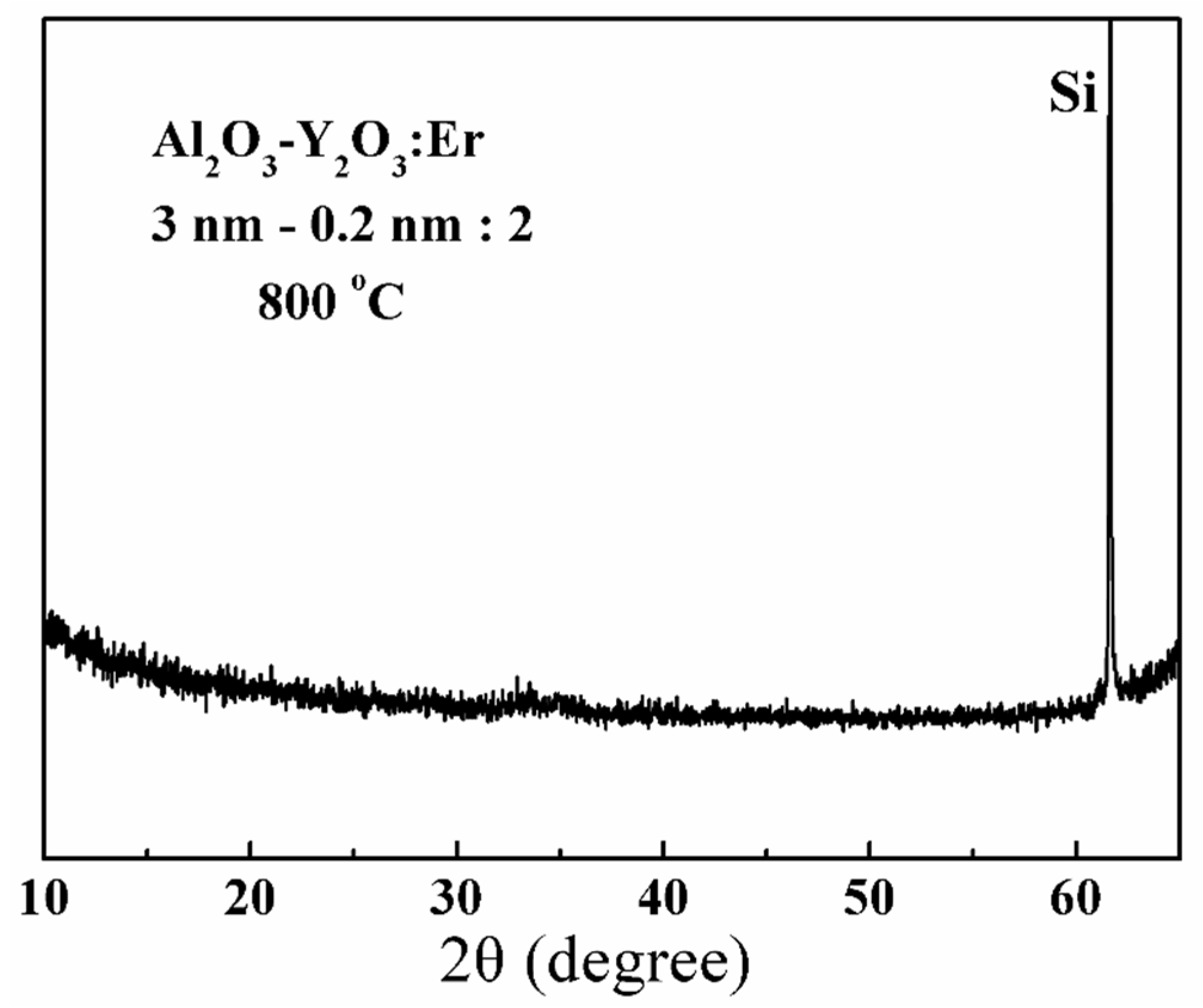
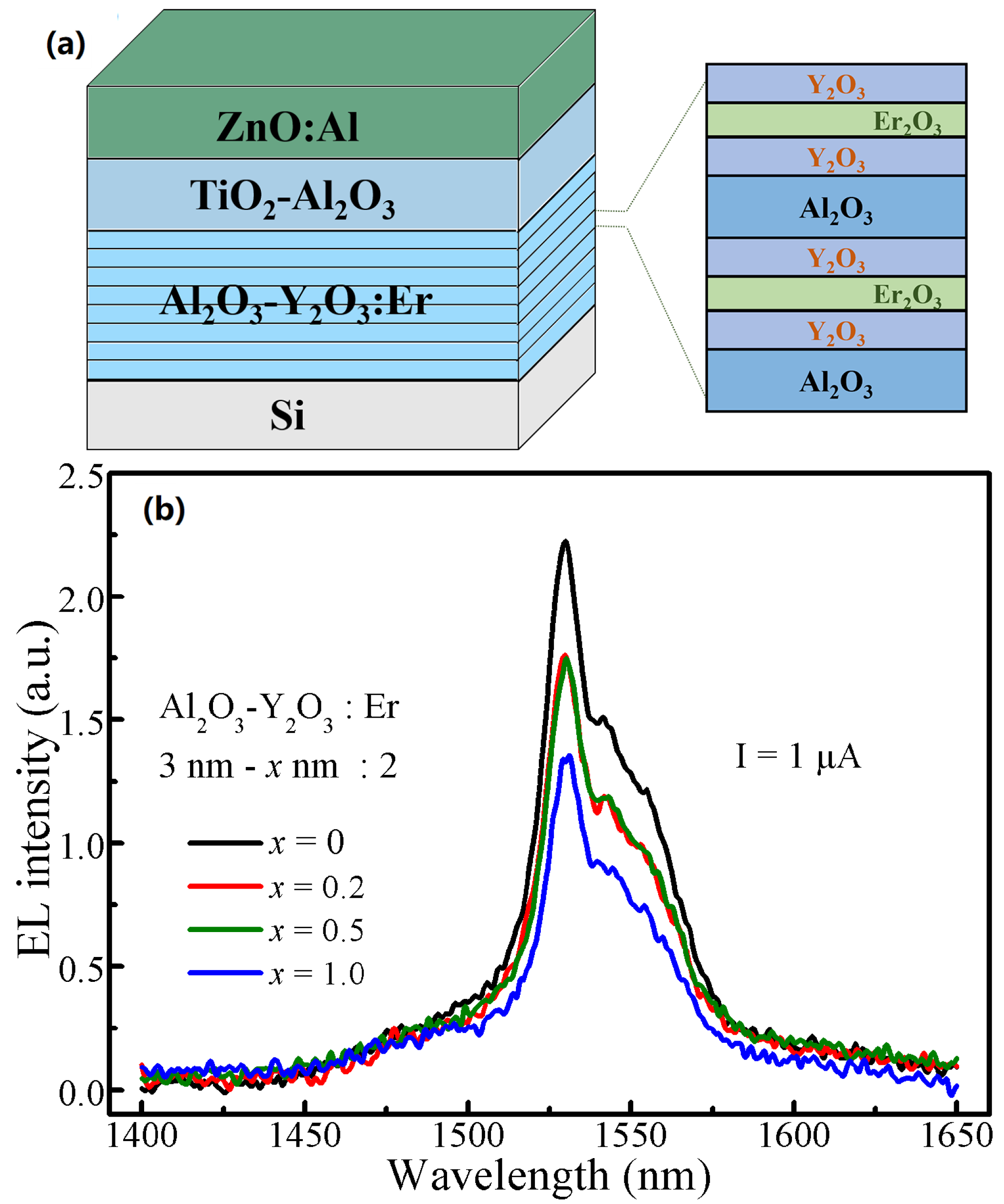
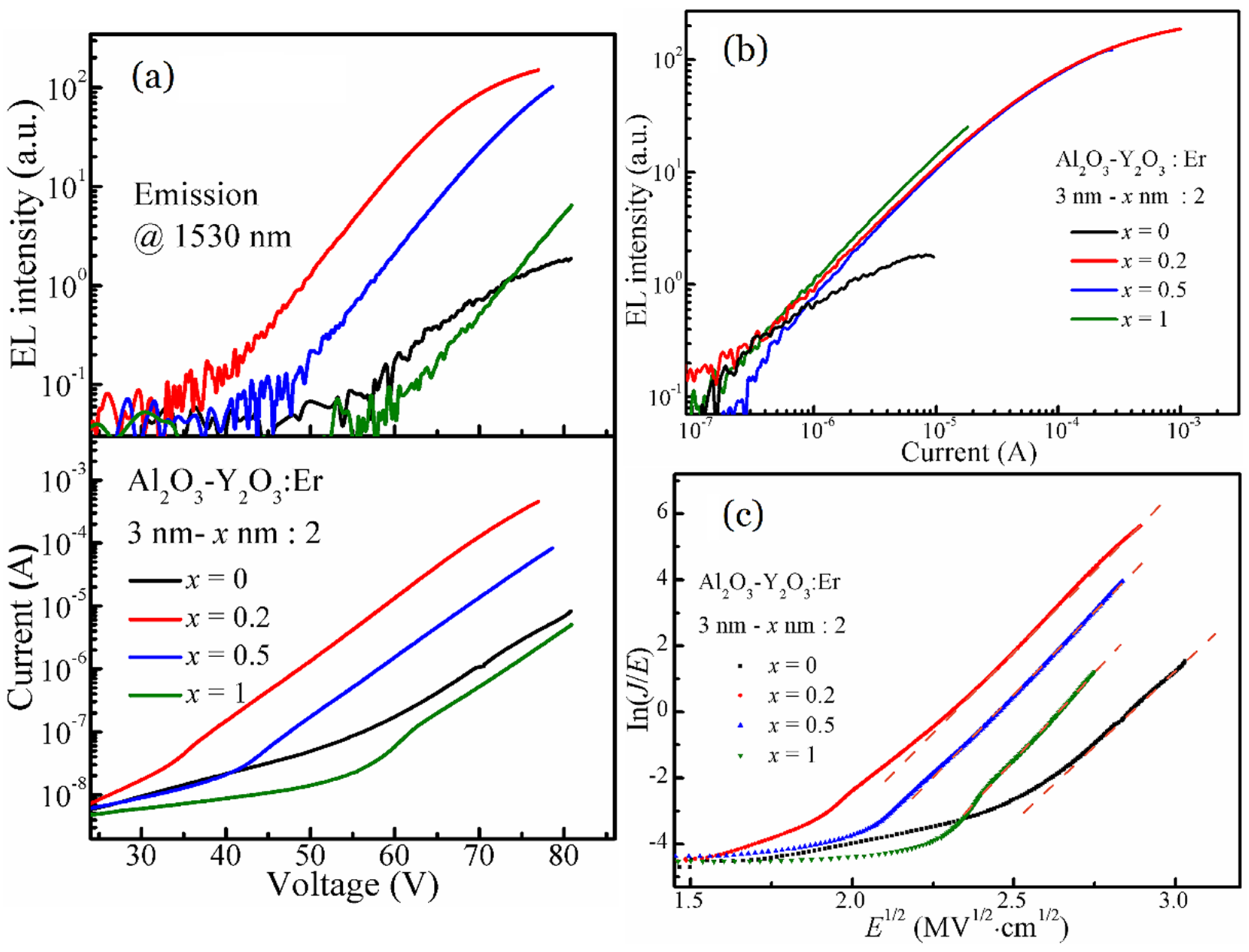
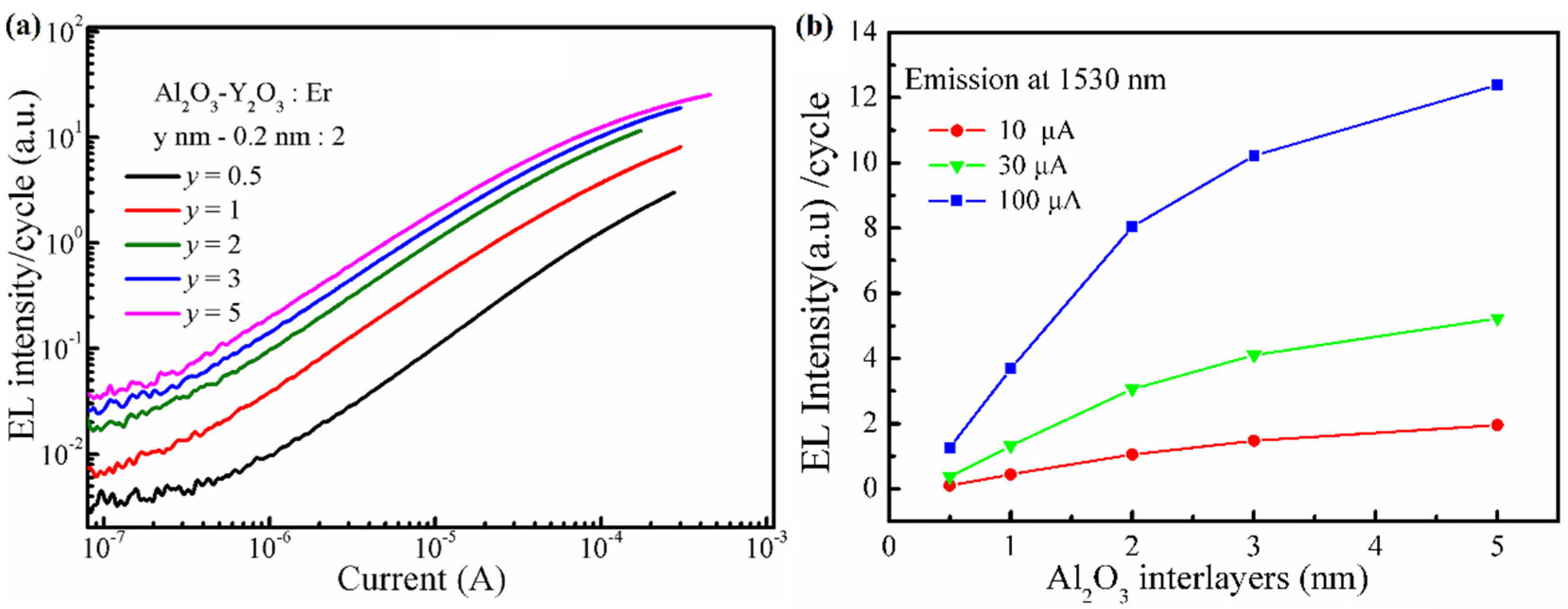
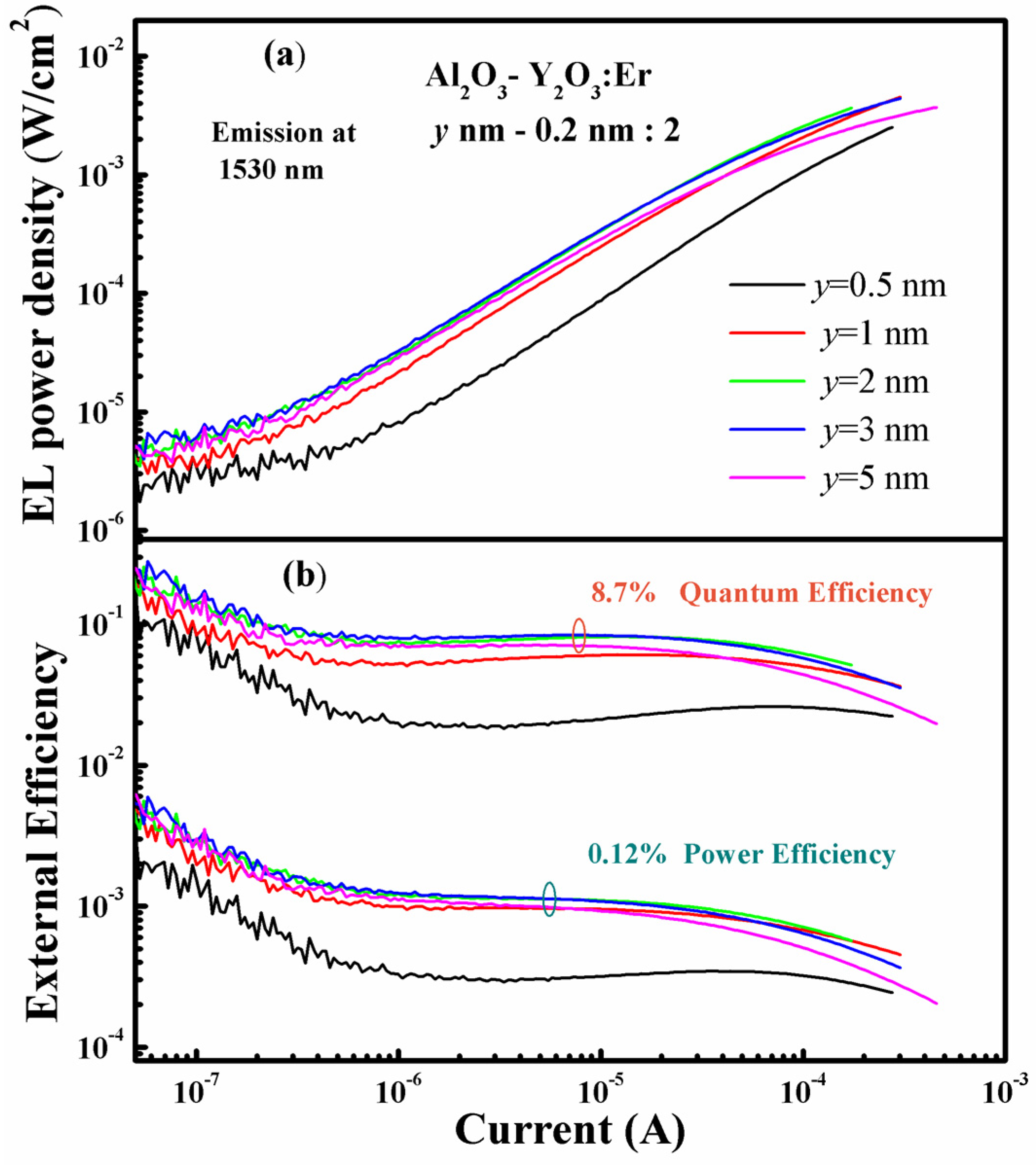
3. Results and Discussion

The XRD patterns of all the Al2O3-Y2O3:Er films annealed at 800 °C confirm that the nanolaminates are amorphous, one representative XRD pattern from the nanolaminate using 3 nm Al2O3 interlayers and 0.2 nm Y2O3 cladding layers is shown in Figure 1. The Al2O3 layers are not crystalized at such a relatively low temperature of 800 °C that beneficial for the EL performance from RE-doped Al2O3 films, while the crystallization of the sub-nanometer Y2O3 layers is restricted [17,20]. The amorphous nanolaminate films are quite smooth under the observation of scanning electron microscope, with a root-square roughness of only 0.56–0.7 nm scanned by the atomic force microscopy (AFM, Dimension Icon, Bruker) [21].
Figure 2a illustrates the schematic diagram for the MOSLEDs and the structure and deposition sequence of the luminescent nanolaminates. Figure 2b shows the NIR EL spectra of MOSLEDs based on the Al2O3-Y2O3:Er films of different Y2O3 cladding layers (with the thickness of x nm). The EL peaks centered at ~1530 nm correspond to the infra-4f 4I13/24I15/2 transitions of the Er3+ ions. The presence of other shoulder peaks is ascribed to the splitting levels associated with the Stark effect [22]. These EL peaks are similar in positions and sharps in the Al2O3-Y2O3:Er nanofilms with different Y2O3 cladding layers, thus the incorporation of Y2O3 cladding layers imposes no apparent effect on the Er3+ intra-4f transitions. In comparison with the Er-emissions from different matrices, the spectra also confirm that the Al2O3-Y2O3:Er films are amorphous due to the absence of companion peaks [20,23].
Figure 3a presents the dependence of the 1530 nm EL intensities and the injection currents on the applied voltages for the Al2O3-Y2O3:Er MOSLEDs with different Y2O3 cladding layers (with the thickness of x nm). These EL–V and I–V curves are similar with our previous reports on the MOSLEDs based on RE-doped oxides, with the typical characteristic of MOS structures [13,18,24,25]. Beneath the threshold electric field, the defect states contribute to the low background currents. In the working voltage region, the currents increase exponentially until breakdown. The difference on the current injection will be discussed afterwards concerning the conduction mechanism. All the EL intensities also present an exponential relationship with the applied voltages until reaching saturation. The MOSLED with 0.2 nm Y2O3 cladding layers presents the highest EL intensity, with the lowest threshold voltage and the highest injection current. The devices with thicker Y2O3 layers underperform in EL intensities and the injection currents are restricted. Despite the uncertainty brought about by the device preparation, Y2O3 cladding layers with suitable thickness can effectively enhance the current injection and promote the EL emissions from these Al2O3-Y2O3:Er MOSLEDs. As previously reported, the incorporation of Y3+ ion makes the crystal field around Er3+ ions less symmetric and introduces distortion in the crystal field, moreover the Er3+ ions are dispersed to suppress the concentration quenching, resulting in the enhanced radiation probability [26]. Therefore, the 0.2 nm Y2O3 layers act as cladding layers that inhibit the Er-clustering, while the thicker Y2O3 layers inhibit the electron injection, which is ascribed to the higher dielectric index of Y2O3 and the disruptive interfaces among Al2O3 and Y2O3 interlayers.
Figure 3b shows the dependence of EL intensities on the injection currents for the Al2O3-Y2O3:Er MOSLEDs with different Y2O3 cladding layers. The threshold currents for all the devices are ~0.2 μA, the EL intensities and the injection currents present linear relationship. In comparison, the devices with different Y2O3 cladding layers exhibit similar EL, which increases more prominently than that based on the Al2O3:Er film. Y2O3 also lessens the saturation of EL intensities at higher injection currents. Considering the thick interlayers among RE layers (the Al2O3 interlayers with the thickness of at least 3 nm), the acceleration distance for hot electrons is sufficient; therefore the enhanced EL should result from more optical-active Er dopants as the Er3+ ions disperse into the Y2O3 layers and the Er-clustering is suppressed.
In our previously reported MOSLEDs based on RE-doped Al2O3, the RE-related EL is triggered by the direct impact excitation of the RE ions by the hot electrons accelerated under sufficient bias voltages [12,25]. As the I–V characterization are accordingly comparable, it is rational to ascribe the NIR EL from these Al2O3-Y2O3:Er MOSLEDs to the same mechanism. Considering the high bandgap of the matrix materials and the barrier for electrons to be injected from the Si substrates into the conduction band of the oxides, the current conduction of these MOSLEDs has been ascribe to the Poole-Frenkel (P-F) mechanism, in which the electrons hop via the defect-related trap states under sufficient electrical field [11,26,27]. In simplicity, the plot of the ln(J/E) versus E1/2 presents linear relationship in P-F conduction mechanism, where J and E are the current density and the electric field, respectively [28,29]. Figure 3c shows the plots of the I–V characteristics derived from Figure 3a, the electrical fields across the luminescent films are roughly calculated in terms of electrostatics [30], and the well-defined linearity is established for all the MOSLEDs in the EL-enabling region. Thus the electron transport through the Al2O3-Y2O3:Er nanofilms is governed by the P-F mechanism. These electrons tunnel into the conduction band of oxides and transport by hopping among trap states in the Al2O3-Y2O3 nanolaminates under sufficient electric field. Certain parts of the electrons are accelerated therein and become hot electrons that excite the Er3+ ions by inelastic impact, the subsequent recombination gives rise to the characteristic EL emissions. Apparently, the Y2O3 cladding layers decrease the working electric field prominently. As mentioned in the discussion on the I–V characteristics, the Y2O3 cladding layers increase both the injection currents and EL intensities, we conclude that ultrathin Y2O3 layers introduce defect sites within Al2O3, via which electrons transport by the P-F hopping mechanism; therefore the injection currents are enhanced. Since the accelerated electrons collide with the doped Er3+ ions and contribute to the NIR EL, adding the aforementioned crystal field distortion and cluster dispersion effects of the Y2O3 on Er3+ ions, the EL performance are greatly enhanced by the Y2O3 cladding layers in Al2O3 films. However, the Y2O3 cladding layers should be thin enough to not impact the carrier transport which could be ascribed to the formation of distinct Al2O3-Y2O3 interfaces when using thicker Y2O3 cladding layers.
In evaluation of the thickness of Al2O3 interlayers on the EL performance, the dependence of the EL intensities from each dopant cycle on the injection currents for the Al2O3-Y2O3:Er MOSLEDs with different Al2O3 interlayers (with the thickness of y nm) are shown in Figure 4a, the thickness of Y2O3 cladding layers is the optimal 0.2 nm. Again, the EL intensities increase almost linearly with the injection currents. The difference on the EL–I–V characteristics among these MOSLEDs with different Al2O3 layers are small (not shown herein), and the increase in EL intensity with the Al2O3 thickness could be ascribed to the less concentration quenching of doped Er3+ ions together with the longer acceleration distance. When the thickness of Al2O3 declines, the EL intensity decreases greatly due to the cross-relaxation of Er3+ between adjacent dopant layers when the inter-distance (the Al2O3 thickness) is smaller enough, and the limited acceleration length for the hot electrons to gain energy to excite the Er3+ ions [18,21,31,32,33]. Cross-relaxation is a common phenomenon that occurs among the same ions or different ions of similar energy intervals. One ion in the excited state (4I13/2 in the case of Er3+ ion) transfer the energy to another one (in the ground state of 4I15/2 in this case of Er3+ ions), excite the latter to higher energy levels (4I13/2) while relaxing itself to lower energy levels (4I15/2) without radiation. The interaction of energy transfer by cross-relaxation could finally disperse the excitation energy through phonons instead of luminescent emissions.
In the RE-doped Al2O3 MOSLEDs, the Al2O3 sublayer thickness affects the cross relaxation between excited RE ions, and the acceleration distance for injected electrons. Figure 4b shows the dependence of the integrated 1530 nm EL intensity per Er cycle on the thickness of Al2O3 interlayers under different injection currents. Under all these injection currents, with the increase in the thickness of Al2O3 interlayers, the contribution of single Er cycle to the EL intensity firstly increases and then saturates as the Al2O3 interlayer thickness reaches 3 nm. This is still in consistency with the common characteristic for the luminescent RE3+ ions in Al2O3 matrix that the distance for the presence of non-radiative interaction and adequate electron acceleration is around 3 nm [11,12,21,33].
Considering the total EL intensity from the MOSLEDs with Al2O3 interlayers of different thicknesses (marked as y nm here) shown in Figure 5a, the device using 3 nm Al2O3 interlayers presents the optimal emission intensity in the operation range, with the highest power density of 4.6 mW/cm2. External efficiency is widely used to evaluate LED performance. Figure 5b shows the EQE and PE of these MOSLEDs based on different Al2O3-Y2O3:Er nanolaminate films. These EL efficiencies sustain a broad maximum, and fall down at higher currents. Generally, the EQE of the devices with 2–3 nm Al2O3 interlayers are the highest. As aforementioned, this phenomenon could be ascribed to the sufficient distance for electron acceleration and suppression of the cross-relaxation among adjacent Er2O3 dopant layers. The Y2O3 cladding layers somewhat decrease this critical distance which is beneficial for higher doping concentrations. The optimal device with 3/0.2 nm Al2O3/Y2O3 interlayers achieves the maximum EQE of 8.7% and a corresponding PE of 0.12%. These values are comparable to our Yb2O3:Er MOSLEDs but with lowered working voltages. In comparison, the control Al2O3:Er MOSLED presents only an EQE of 3% and a PE of 0.014%, much lower than the Al2O3-Y2O3:Er MOSLEDs. The Y2O3 cladding layers with suitable thickness enhance the efficiencies from the MOSLEDs to a great extent. We have found that by using a thicker luminescent layer, the efficiency of the Al2O3:RE MOSLED might be further increased to higher than 10% [25,34]. These efficiencies are superior to that from Si-based EL devises in literature, thus further optimization of the luminescent Al2O3-Y2O3:Er nanolaminates would supply potential light source for the applications in Si-based optoelectronics.

4. Conclusions

In summary, significantly enhanced ~1530 nm NIR EL emissions are achieved from the MOSLEDs based on the amorphous Al2O3:Er nanolaminate films by the insertion of cladding Y2O3 sub-nanolayers, which are fabricated by ALD on Si substrates. The Y2O3 cladding layers reduce the threshold electric field for excitation and increase the radiative possibility of doped Er3+ ions, resulting in improved EL performance. The Al2O3-Y2O3:Er MOSLEDs with 0.2 nm Y2O3 and 3 nm Al2O3 interlayers present an EQE of 8.7% and a corresponding PE of 0.12%, which are much higher than that of the counterpart without Y2O3 cladding layers. The incorporation of Y2O3 does not change the electron injection mode under sufficient electric field that conforms to P-F mechanism, the resultant energetic electrons trigger the impact-excitation of Er3+ ions and subsequent EL emissions. The strategy of Y2O3-cladding by ALD can be employed to improve the EL performance from LEDs based on RE-doped oxides.

Author Contributions

Conceptualization, Y.Y. and J.S.; Methodology, H.P.; Validation, H.P. and Y.Y.; Formal analysis, H.P. and Y.Y.; Resources, Y.Y. and J.S.; Data curation, H.P. and Y.Y.; Writing-original draft preparation, Y.Y., H.P. and Z.Y.; Writing-review and editing, Y.Y.; Visualization, H.P. and Z.Y.; Supervision, Y.Y. and J.S.; Project administration, J.S.; Funding acquisition, Y.Y. and J.S. All authors have read and agreed to the published version of the manuscript.

Funding

This research was funded by the National Natural Science Foundation of China (No. 62275132 and 61705114).

Data Availability Statement

Data will be made available on request.

Conflicts of Interest

The authors declare no competing financial interest.

References

  1. Bogaerts, W.; Chrostowski, L. Silicon Photonics Circuit Design: Methods, Tools and Challenges. Laser Photonics Rev. 2018, 12, 1700237. [Google Scholar] [CrossRef] [Green Version]
  2. Crosnier, G.; Sanchez, D.; Bouchoule, S.; Monnier, P.; Beaudoin, G.; Sagnes, I.; Raj, R.; Raineri, F. Hybrid indium phosphide-on-silicon nanolaser diode. Nat. Photonics 2017, 11, 297–300. [Google Scholar] [CrossRef]
  3. Sarkar, A.; Lee, Y.; Ahn, J.-H. Si nanomebranes: Material properties and applications. Nano Res. 2021, 14, 3010–3032. [Google Scholar] [CrossRef]
  4. Makarova, M.; Sih, V.; Warga, J.; Li, R.; Dal Negro, L.; Vuckovic, J. Enhanced light emission in photonic crystal nanocavities with Erbium-doped silicon nanocrystals. Appl. Phys. Lett. 2008, 92, 161107. [Google Scholar] [CrossRef] [Green Version]
  5. Yang, Y.; Jin, L.; Ma, X.; Yang, D. Low-voltage driven visible and infrared electroluminescence from light-emitting device based on Er-doped TiO2/p+-Si heterostructure. Appl. Phys. Lett. 2012, 100, 031103. [Google Scholar] [CrossRef]
  6. Hernández Simón, Z.J.; Luna López, J.A.; de la Luz, A.D.; Pérez García, S.A.; Benítez Lara, A.; García Salgado, G.; Carrillo López, J.; Mendoza Conde, G.O.; Martínez Hernández, H.P. Spectroscopic Properties of Si-nc in SiOx Films Using HFCVD. Nanomaterials 2020, 10, 1415. [Google Scholar] [CrossRef] [PubMed]
  7. Yang, Y.; Li, Y.; Wang, C.; Zhu, C.; Lv, C.; Ma, X.; Yang, D. Rare-Earth Doped ZnO Films: A Material Platform to Realize Multicolor and Near-Infrared Electroluminescence. Adv. Opt. Mater. 2014, 2, 240–244. [Google Scholar] [CrossRef]
  8. Guo, Y.; Lin, Z.X.; Huang, R.; Lin, Z.W.; Song, C.; Song, J.; Wang, X. Efficiency enhancement for SiN-based light emitting device through introduction of Si nanocones in emitting layer. Opt. Mater. Express 2015, 5, 969–976. [Google Scholar] [CrossRef]
  9. Patra, A.; Friend, C.S.; Kapoor, R.; Prasad, P.N. Upconversion in Er3+:ZrO2 Nanocrystals. J. Phys. Chem. B 2002, 106, 1909–1912. [Google Scholar] [CrossRef]
  10. Wang, X.J.; Yuan, G.; Isshiki, H.; Kimura, T.; Zhou, Z. Photoluminescence enhancement and high gain amplification of ErxY2−xSiO5 waveguide. J. Appl. Phys. 2010, 108, 013506. [Google Scholar] [CrossRef]
  11. Yang, Y.; Li, N.; Sun, J. Intense electroluminescence from Al2O3/Tb2O3 nanolaminate films fabricated by atomic layer deposition on silicon. Opt. Express 2018, 26, 9344–9352. [Google Scholar] [CrossRef]
  12. Ouyang, Z.; Yang, Y.; Sun, J. Near-infrared electroluminescence from atomic layer doped Al2O3:Yb nanolaminate films on silicon. Scr. Mater. 2018, 151, 1–5. [Google Scholar] [CrossRef]
  13. Wang, Y.; Yu, Z.; Yang, Y.; Sun, J. Bright red electroluminescence from Al2O3/Eu2O3 nanolaminate films fabricated by atomic layer deposition on silicon. Scr. Mater. 2021, 196, 113750. [Google Scholar] [CrossRef]
  14. Rönn, J.; Karvonen, L.; Kauppinen, C.; Perros, A.P.; Peyghambarian, N.; Lipsanen, H.; Säynätjoki, A.; Sun, Z. Atomic Layer Engineering of Er-Ion Distribution in Highly Doped Er:Al2O3 for Photoluminescence Enhancement. ACS Photonics 2016, 3, 2040–2048. [Google Scholar] [CrossRef]
  15. Leskelä, M.; Ritala, M. Atomic layer deposition (ALD): From precursors to thin film structures. Thin Solid Film. 2002, 409, 138–146. [Google Scholar] [CrossRef]
  16. Lee, D.-J.; Kim, H.-M.; Kwon, J.-Y.; Choi, H.; Kim, S.-H.; Kim, K.-B. Structural and Electrical Properties of Atomic Layer Deposited Al-Doped ZnO Films. Adv. Funct. Mater. 2011, 21, 448–455. [Google Scholar] [CrossRef]
  17. Ouyang, Z.; Yang, Y.; Sun, J. Electroluminescent Yb2O3:Er and Yb2Si2O7:Er nanolaminate films fabricated by atomic layer deposition on silicon. Opt. Mater. 2018, 80, 209–215. [Google Scholar] [CrossRef]
  18. Liu, Y.; Ouyang, Z.; Yang, L.; Yang, Y.; Sun, J. Blue Electroluminescent Al2O3/Tm2O3 Nanolaminate Films Fabricated by Atomic Layer Deposition on Silicon. Nanomaterials 2019, 9, 413. [Google Scholar] [CrossRef] [Green Version]
  19. Tuomisto, M.; Giedraityte, Z.; Karppinen, M.; Lastusaari, M. Photon up-converting (Yb,Er)2O3 thin films by atomic layer deposition. Phys. Status Solidi RRL 2017, 11, 1700076. [Google Scholar] [CrossRef]
  20. Xu, J.; Liu, J.; Yang, L.; Liu, J.; Yang, Y. Electroluminescent Y3Al5O12 nanofilms fabricated by atomic layer deposition on silicon: Using Yb as the luminescent dopant and crystallization impetus. Opt. Express 2021, 29, 37–47. [Google Scholar] [CrossRef] [PubMed]
  21. Liu, J.; Liu, Y.; Yang, Y.; Sun, J. Exploration of the green electroluminescence from Al2O3/Ho2O3 nanolaminate films fabricated by atomic layer deposition on silicon. Opt. Mater. 2020, 107, 110125. [Google Scholar] [CrossRef]
  22. Gruber, J.B.; Burdick, G.W.; Chandra, S.; Sardar, D.K. Analyses of the ultraviolet spectra of Er3+ in Er2O3 and Er3+ in Y2O3. J. Appl. Phys. 2010, 108, 023109. [Google Scholar] [CrossRef] [Green Version]
  23. Xu, J.; Yang, L.; Ma, Z.; Yang, Y.; Sun, J. Electroluminescent polycrystalline Er-doped Lu3Al5O12 nanofilms fabricated by atomic layer deposition on silicon. J. Alloys Compd. 2021, 885, 160993. [Google Scholar] [CrossRef]
  24. Sun, J.M.; Skorupa, W.; Dekorsy, T.; Helm, M.; Rebohle, L.; Gebel, T. Bright green electroluminescence from Tb3+ in silicon metal-oxide-semiconductor devices. J. Appl. Phys. 2005, 97, 123513. [Google Scholar] [CrossRef] [Green Version]
  25. Sun, J.M.; Rebohle, L.; Prucnal, S.; Helm, M.; Skorupa, W. Giant stability enhancement of rare-earth implanted SiO2 light emitting devices by an additional SiON protection layer. Appl. Phys. Lett. 2008, 92, 071103. [Google Scholar] [CrossRef] [Green Version]
  26. Jiang, M.; Zhu, C.; Zhou, J.; Chen, J.; Gao, Y.; Ma, X.; Yang, D. Electroluminescence from light-emitting devices with erbium-doped TiO2 films: Enhancement effect of yttrium codoping. J. Appl. Phys. 2016, 120, 163104. [Google Scholar] [CrossRef]
  27. Rebohle, L.; Braun, M.; Wutzler, R.; Liu, B.; Sun, J.M.; Helm, M.; Skorupa, W. Strong electroluminescence from SiO2-Tb2O3-Al2O3 mixed layers fabricated by atomic layer deposition. Appl. Phys. Lett. 2014, 104, 251113. [Google Scholar] [CrossRef]
  28. Samanta, P.; Mandal, K.C. Hole injection and dielectric breakdown in 6H-SiC and 4H-SiC metal-oxide-semiconductor structures during substrate electron injection via Fowler–Nordheim tunneling. Solid State Electron. 2015, 114, 60–68. [Google Scholar] [CrossRef]
  29. Zheng, C.Y.; He, G.; Chen, X.F.; Liu, M.; Lv, J.G.; Gao, J.; Zhang, J.W.; Xiao, D.Q.; Jin, P.; Jiang, S.S.; et al. Modification of band alignments and optimization of electrical properties of InGaZnO MOS capacitors with high-k HfOxNy gate dielectrics. J. Alloys Compd. 2016, 679, 115–121. [Google Scholar] [CrossRef]
  30. Kim, W.; Park, S.I.; Zhang, Z.; Wong, S. Current Conduction Mechanism of Nitrogen-Doped AlOx RRAM. IEEE Trans. Electron Devices 2014, 61, 2158–2163. [Google Scholar] [CrossRef]
  31. Zhu, C.; Lv, C.; Gao, Z.; Wang, C.; Li, D.; Ma, X.; Yang, D. Multicolor and near-infrared electroluminescence from the light-emitting devices with rare-earth doped TiO2 films. Appl. Phys. Lett. 2015, 107, 131103. [Google Scholar] [CrossRef]
  32. Kim, Y.S.; Yun, S.J. Studies on polycrystalline ZnS thin films grown by atomic layer deposition for electroluminescent applications. Appl. Surf. Sci. 2004, 229, 105–111. [Google Scholar] [CrossRef]
  33. Yuan, K.; Liu, Y.; Ou-Yang, Z.T.; Liu, J.; Yang, Y.; Sun, J. Resonant energy transfer between rare earth atomic layers in nanolaminate films. Opt. Lett. 2022, 47, 4897–4900. [Google Scholar] [CrossRef] [PubMed]
  34. Yang, Y.; Ouyang, Z.; Liu, J.; Sun, J. Energy Transfer under Electrical Excitation and Enhanced Electroluminescence in the Nanolaminate Yb,Er Co-Doped Al2O3 Films. Phys. Status Solidi RRL 2019, 13, 1900137. [Google Scholar] [CrossRef]
Figure 1. The XRD pattern for the representative Al2O3-Y2O3:Er nanolaminate film after annealing at 800 °C.
Nanomaterials 13 00849 g001
Figure 2. (a) The schematic diagram for the Al2O3-Y2O3:Er MOSLEDs and the luminescent nanolaminate films. (b) The NIR EL spectra for the Al2O3-Y2O3:Er MOSLEDs with different Y2O3 cladding layers (with the thickness of x nm) under the injection current of 1 μA.
Nanomaterials 13 00849 g002
Figure 3. (a) The dependence of EL intensities and injection currents on the applied voltage for the Al2O3-Y2O3:Er MOSLEDs with different Y2O3 interlayers (with the thickness of x nm), and (b) the dependence of EL intensities on the injection currents for these devices. (c) The plot of ln(J/E) versus E1/2 (P–F plots of the I–V characteristics) for the Al2O3-Y2O3:Er MOSLEDs with different Y2O3 interlayers.
Nanomaterials 13 00849 g003
Figure 4. (a) The dependence of EL intensities on the injection currents for the Al2O3-Y2O3:Er MOSLEDs with different Al2O3 interlayers (with the thickness of y nm), herein the EL intensities are divided by the cycle numbers to manifest the emissions from each Er cycle. (b) The integrated EL intensity per cycle as a function of the thickness of the Al2O3 interlayers under different injection currents.
Nanomaterials 13 00849 g004
Figure 5. The dependence of (a) the EL power densities and (b) the external quantum efficiencies (the upper curves) and power efficiencies (the lower curves) on the injection currents for Al2O3-Y2O3:Er MOSLEDs using different Al2O3 interlayers (with the thickness of y nm).
Nanomaterials 13 00849 g005
Disclaimer/Publisher’s Note: The statements, opinions and data contained in all publications are solely those of the individual author(s) and contributor(s) and not of MDPI and/or the editor(s). MDPI and/or the editor(s) disclaim responsibility for any injury to people or property resulting from any ideas, methods, instructions or products referred to in the content.

