Article

Influence of Different Carrier Gases, Temperature, and Partial Pressure on Growth Dynamics of Ge and Si Nanowires

1
Department of Physics, University of Basel, Klingelbergstrasse 82, CH-4056 Basel, Switzerland
2
Swiss Nanoscience Institute, University of Basel, Klingelbergstrasse 82, CH-4056 Basel, Switzerland
*
Author to whom correspondence should be addressed.
Nanomaterials 2023, 13(21), 2879; https://doi.org/10.3390/nano13212879
Submission received: 2 October 2023 / Revised: 23 October 2023 / Accepted: 29 October 2023 / Published: 30 October 2023
(This article belongs to the Special Issue Preparation and Application of Nanowires II)

Abstract

:
The broad and fascinating properties of nanowires and their synthesis have attracted great attention as building blocks for functional devices at the nanoscale. Silicon and germanium are highly interesting materials due to their compatibility with standard CMOS technology. Their combination provides optimal templates for quantum applications, for which nanowires need to be of high quality, with carefully designed dimensions, crystal phase, and orientation. In this work, we present a detailed study on the growth kinetics of silicon (length 0.1–1 μ m, diameter 10–60 nm) and germanium (length 0.06–1 μ m, diameter 10–500 nm) nanowires grown by chemical vapor deposition applying the vapour–liquid–solid growth method catalysed by gold. The effects of temperature, partial pressure of the precursor gas, and different carrier gases are analysed via scanning electron microscopy. Argon as carrier gas enhances the growth rate at higher temperatures (120 nm/min for Ar and 48 nm/min H 2 ), while hydrogen enhances it at lower temperatures (35 nm/min for H 2 and 22 nm/min for Ar) due to lower heat capacity. Both materials exhibit two growth regimes as a function of the temperature. The tapering rate is about ten times lower for silicon nanowires than for germanium ones. Finally, we identify the optimal conditions for nucleation in the nanowire growth process.

1. Introduction

Nanowires (NW) have gained a great deal of attention in the last decades due to their fascinating properties, e.g., large surface-to-volume ratio [1,2], quantum confinement of charge carriers [3,4], and high carrier mobility [5]. These properties, if controlled on demand, can be used to engineer building blocks of functional devices at the nanoscale, finding applications in, e.g., optoelectronics [6,7], electronics [6,8], and photovoltaics [9,10,11]. To this end, control of the dimensions, crystal orientation, crystal phase, and density of crystal defects is crucial. The electrical properties of graphene sheets [12], organic molecules [12], and semiconductor nanowires [13] have been studied; however, most of these systems are not compatible with complementary metal oxide semiconductor (CMOS) technology, and as such are less likely to be incorporated into well-established fabrication processes.
Group IV materials, in particular germanium (Ge) and silicon (Si), offer potential ease of integration for the microelectronics industry [7,14,15,16]. The structural and electrical properties of Si nanowires [2,11] and the intrinsic high carrier mobility of Ge nanowires [17,18,19,20,21] make the combination of these two materials a perfect template for photodetection [2,22,23], energy storage [24,25], and quantum computing [26,27,28]. In order to integrate nanowires into large-scale applications and complex architectures, a high level of control of the growth mechanism is needed.
Theoretical modelling and understanding of the change of properties when switching from the bulk to the nanometer scale is of great value for further optimisation of the growth process. Using first principles calculations has already shown good predictive results [29]. Different materials have been modelled, including Ge [30,31,32], Si [30,33,34], SiGe [30,35,36], ZnO [37,38], GaAs [39], and InN [40]. Despite the huge application potential of Ge and Si nanowires, no theoretical publications have yet shed light on the influence of their growth parameters. Recent research has focused mostly on investigating the properties of Ge and Si nanowires, with particular emphasis on their electrical [38,41,42,43,44], thermal [45,46], and optical properties [38,47,48].
Nanowires can be grown using a top-down or bottom-up approach [12,49,50,51]. Usually, bottom-up nanowires are grown via the so-called vapour–liquid–solid (VLS) approach [49,52,53,54,55], which was first reported in 1964 [56]. The VLS method offers the unique possibility of merging a large variety of material combinations, which is due to the strain relaxation mechanism in nanowires [57,58]. The effectiveness of VLS has been demonstrated for a wide range of combinations already [59,60,61,62,63,64]. In VLS, a metallic nanoparticle, e.g., gold, is used to catalyze growth. This nanoparticle forms a liquid eutectic droplet with the underlying substrate at the eutectic temperature. The precursor gas decomposes onto the surface of the liquid catalyst and starts to accumulate inside the liquid droplet upon supersaturation. At this point, the wires start to precipitate in a layer-by-layer manner at the interface between the catalyst and the substrate; the diameter of the nanowire is defined by the catalyst droplet size [65,66]. Different metals can be used as catalysts, with one of the most common for Si and Ge nanowires being gold. The catalyst droplet can be obtained either as the result of dewetting a thin film [67,68], as a lithographically fabricated nanoparticle array [69,70], or by depositing a colloidal solution on the substrate [54,71,72]. Gold has proven to be an ideal catalyst for hydride precursors; it is redox-inactive [73], exhibits a relatively low eutectic temperature, and has many key semiconducting materials, including silicon and germanium. For Si and Ge in combination with Au, the eutectic temperature is around 360 ° C [74,75,76,77,78,79].
Different techniques can be used to grow NWs, mainly differing in the way that the precursor is provided to the catalyst, with examples including metal–organic chemical vapour deposition, molecular beam epitaxy, and chemical vapour deposition (CVD). CVD is a commonly used technique to grow nanowires [6,18,51,68,80], offering epitaxial growth along with the required control over size, composition, and morphology. In order to grow high quality nanowires, it is vital to understand the influence of the growth conditions. Because CVD offers a large parameter space in terms of growth conditions, a thorough investigation of their impact on nanowire morphology and crystal properties is necessary. In this article, we present a systematic study of Si and Ge nanowire growth conditions. The wires were grown onto an Si <100> substrate via VLS using gold as catalyst. The effects of temperature and partial pressure were evaluated, and the influence of carrier gases was considered. To the best of our knowledge, no previous studies have provided these insights into the effects of carrier gases on the growth of nanowires using these materials.

2. Materials and Methods

The nanowires (NWs) used in this study were all grown using the VLS approach under a gold-catalysed reaction. The sample preparation prior to growth can be described in two steps. In the first step, gold nanoparticles with a diameter of 5 nm were deposited onto an undoped Si <100> substrate (float zone, undoped, resistivity > 10 , 000 Ohm cm , UniversityWafer Inc., South Boston, MA, USA) from a commercial colloidal suspension (SPI Supplies and BBI Solutions), which was diluted in deionized water in a ratio of 1:10. An electrostatic approach was employed for deposition, which was triggered by the addition of HCl 0.1 M [81]. In the second step, the samples were immersed in a 2% HF aqueous solution for 1 min to remove the native silicon oxide, with a load time after HF etching of no longer than 8 min. Afterwards, the NWs were grown using a PlasmaPro 100 Nanofab reactor from Oxford Instruments, Wiesbaden, Germany (base pressure < 0.5 mTorr ). As the precursor gases, we used commercially available germane gas ( GeH 4 , PanGas AG, Switzerland, 99.999%) and silane gas ( SiH 4 , PanGas AG, Dagmersellen, Switzerland, 99.999%), while we used argon and hydrogen (Ar, H 2 , PanGas AG, Switzerland, 99.999%) as the dilution carrier gases.
The growth protocol consisted of three steps: (i) preheating the chamber to the growth temperature; (ii) loading the sample immediately after HF; and (iii) introduction of the reaction gas mixture, consisting of the precursor gas and carrier gas, subsequent to the loading of the sample. Upon inlet of the gas mixture, the pressure increased to the preset pressure, which depended on the experiment being conducted.
After growth, the NWs were imaged using scanning electron microscopy (SEM) to determine the NW dimensions and orientation. Therefore, the SEM scan direction was oriented parallel to the natural cleaving plane of the Si chip, with the edge lines following ⟨110⟩ directions. Figure 1 shows a top view SEM image of the resulting NWs. We have added an inset in the top right corner of Figure 1 indicating the ⟨110⟩ directions as diagonal lines and the ⟨111⟩ directions as horizontal and vertical lines.
For statistical evaluation of the obtained wires, we defined a protocol with which we analysed three images from different areas of each as-grown sample, which were about 1 to 2 mm apart from each other. We predefined an area (the red rectangle in Figure 1) and considered only those NWs for which growth started inside this area. We manually drew lines according to the growth direction of the wires, taking into account those wires fully contained within the predefined area (the red arrows in Figure 1) and those ending outside the predefined area (the green arrows in Figure 1). Unless otherwise specified, all possible growth directions of the NWs were considered in our statistical analysis of the influence of the growth parameters, although only the main and statistically more probable growth directions (<110> and <111>) are indicated in the inset of Figure 1a. Crossing of NWs was been considered in the statistics according to their base directions. In this way, both the length of the NWs and their orientation was determined while taking into account the length correction due to the projection of the angle of view. We used ImageJ software (Version 1.48s), and the scale was set automatically according to the SEM image. Growth rates were calculated by averaging the individual length of the NWs for each sample and dividing the result by the growth time without differentiating between growth directions.
For the nucleation maps, only the angles representing the <110> ( 45 ± 10 ° ) and <111> ( 0 + 5 ° and 90 5 ° ) growth directions were considered. The colloid density used to calculate the nucleation rates was determined by SEM images of the exemplary samples after deposition of the colloids.

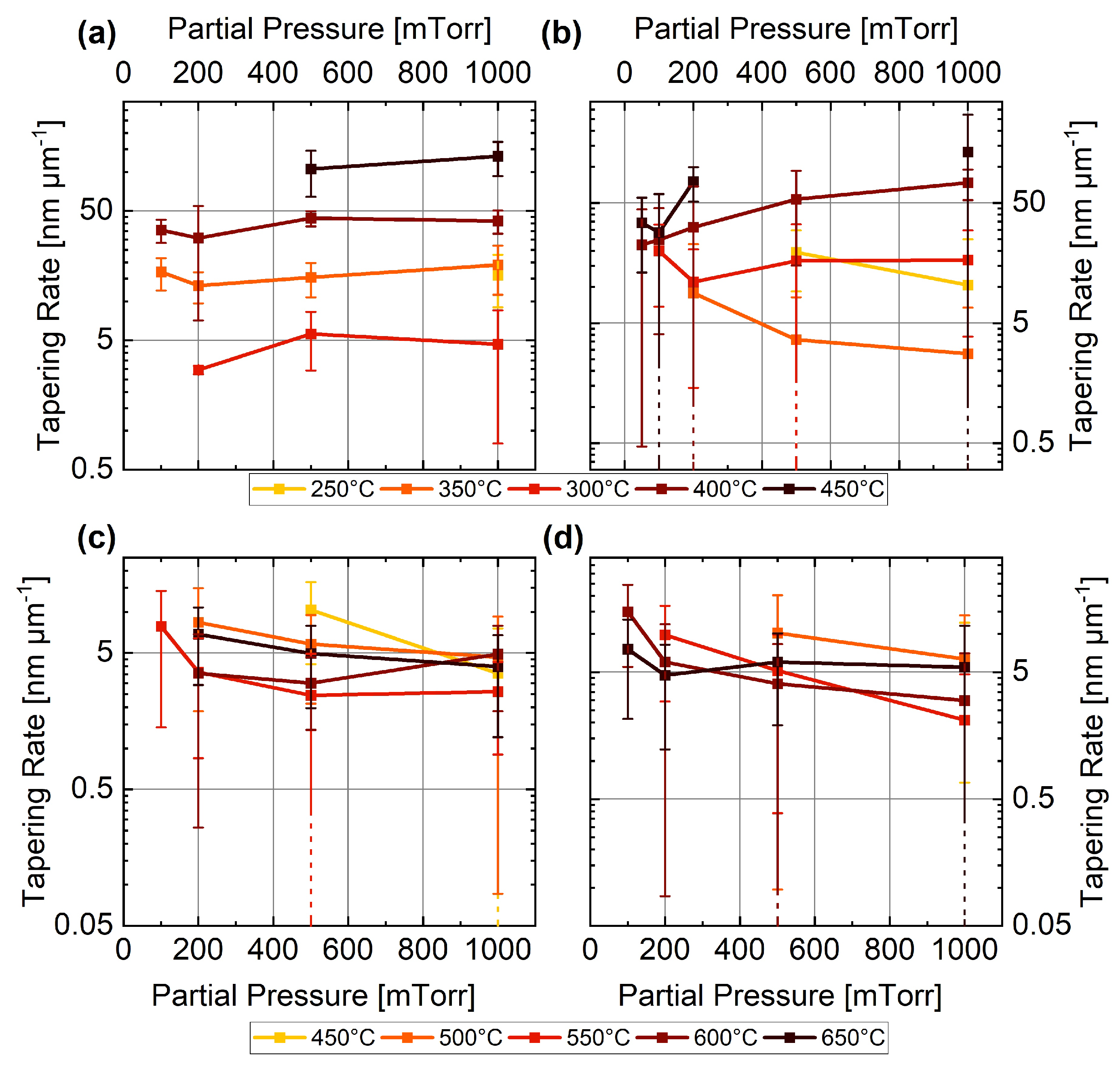
3. Results and Discussion

In order to investigate the influence of partial pressure and temperature on the growth rate and tapering rate of Ge and Si NWs, different growth conditions were evaluated by means of SEM imaging techniques.
In Figure 2, the dependence of the growth rate on the temperature and partial pressure of the precursor gas is presented for 10 % GeH 4 in Ar (a,c,e) and 10 % GeH 4 in H 2 (b,d,f). Qualitatively, a linear behaviour of the growth rate for increasing partial pressure can be observed for both carrier gases (Ar and H 2 in Figure 2a and Figure 2b, respectively). This observation is further highlighted in Figure 2c,d, and is related to a higher rate of Ge being incorporated into the liquid eutectic when the pressure is increased [82]. Interestingly, no growth could be observed when setting a growth temperature of 450 ° C and a partial pressure of 500 mTorr using H 2 as a precursor gas. While the reason for this is not yet clear, this result was reproduced multiple times.
By comparing the results obtained with the two carrier gases, another trend can be identified in Figure 2a,b. When H 2 is used as carrier gas, the growth rate is reduced for higher temperatures (e.g., 48 ± 15 nm/min in H 2 compared to 120 ± 43 nm/min in Ar at 450 ° C and 1 Torr) and enhanced for lower temperatures (e.g., 35 ± 24 nm/min in H 2 compared to 22 ± 15 nm/min in Ar at 300 ° C and 1 Torr). The high-temperature behaviour can be explained by the lower specific heat capacity of H 2 , which results in slower dissociation of GeH 4 and consequently in a reduced growth rate [83]. The low-temperature regime (below 350 ° C) investigated in this study is below the desorption temperature of H 2 [84,85], resulting in a more dominant enhancement of the growth rate. The overall observed growth range is enhanced with H 2 , especially for low partial pressures and high-temperature regions (above 350 ° C).
The growth rate for Si NWs and their dependence on the partial pressure of SiH 4 , temperature, and carrier gas are presented in Figure 3. As gas mixtures, we used 10 % SiH 4 in Ar (a,c,e) and 10 % SiH 4 in H 2 (b,d,f). Similar to the case of the Ge NWs, qualitatively, a linear dependence of the growth rate on pressure is observed for Si NWs (see Figure 3c,d). This dependence is due to a higher incorporation rate of Si into the liquid eutectic [82] at higher pressures. On the other hand, we observed an exponential dependence on temperature when using Ar as the carrier gas and a linear dependence when using H 2 (see Figure 3e and Figure 3f, respectively). This different dependence can be further explained by the larger enhancement of the growth rate with Ar due to its higher specific heat capacity [83].
For both material systems, two different temperature-dependent growth regimes can be identified for higher pressures (Figure 2c,d and Figure 3c,d), as is further discussed below and highlighted in Figure 4.
In the Arrhenius plots in Figure 4, the growth rate is plotted against the inverse of the temperature. Independent of the type of carrier gas, two different growth rate regimes can be observed for high-pressure conditions (partial pressure > 200 mTorr), as highlighted by the light grey line in panels (a) to (d), which indicates the transition temperature. The transition temperatures between the two regimes are at around 350 ° C for Ge NWs and 550 ° C for Si NWs in both Ar and H 2 , which is in good agreement with previously reported experiments [86,87]. These transition temperatures were ascertained using a quantitative method, for which two linear fits in the intervals of (350 ° C, N) and (N, 450 ° C) for Ge NWs and (450 ° C, N) and (N, 650 ° C) for Si NWs were computed, yielding the residual of squares. We linearly fitted the logarithm of the growth rates (data plotted in Figure 4) with the Arrhenius equation provided by
ln growth rate = E A R · 1 T ,
where R is the universal gas constant and E A is the activation energy. The calculated activation energies for the different regimes, precursors, and carrier gases are presented in Table 1.
For the Ge NWs, a lower activation energy can be observed for lower temperature (below 350 ° C) and a higher one for higher temperature (above 350 ° C). The increase in activation energy at higher temperatures can be related to a competing effect between the temperature-dependent decomposition of the precursor gas and the uncatalysed deposition on the side facets and the substrate, resulting in a higher tapering rate, as identified in Figure 2 [88]. The activation energy values of around 90 kJ · mol 1 estimated for GeH 4 for temperatures above 350 ° C (the high temperature in Table 1) are in good agreement with the values reported in the literature [89,90]. The values for the low-temperature region (the low temperature in Table 1) are three to six times smaller compared to the value of 138.07 kJ · mol 1 reported for thin film deposition in [86]. This reduction in activation energy is consistent with a catalysed reaction; therefore, it is coherent with the VLS mechanism leading to NW growth.
Considering the values of the activation energy, the estimate for SiH 4 is about half the value reported in the literature for similar temperature regions, ranging from 89 to 230 kJ · mol 1 below 550 ° C (the low temperature in Table 1) [12,75,87,91,92] and 74 to 89 kJ · mol 1 above 550 ° C (the high temperature in Table 1) [74,93]. However, our results are consistent with the trends observed previously, i.e., higher activation energy for lower temperatures and lower activation energy for higher temperatures. The catalytic effect of Au may be related to the lower activation energy for the lower temperatures compared to the thin film deposition reported in literature, ranging from 125 to 214 kJ · mol 1 [87,91]. Furthermore, it has previously been observed that the activation energy depends on the size of the catalyst [75]. In our study, we used Au particles with a small size (nominal colloid size of 5 nm), further increasing the consistency of our values for the activation energy compared to those reported in literature.
The tapering rates for Ge and Si NWs and their dependence on the partial pressure of GeH 4 and SiH 4 are presented in Figure 5. We used 10 % precursor gas ( GeH 4 and SiH 4 ) in Ar (a,b) and H 2 (c,d) as gas mixtures. Increasing the partial pressure did not have an effect on the tapering rate independent of the type of carrier gas; instead, we observed a dependence of the tapering rate on the temperature, especially for the Ge NWs. This dependence can be explained by the fact that uncatalysed decomposition is less dependent on the pressure, and is mainly dependent on the temperature [82].
Another important aspect of the growth of NWs is the possibility of controlling the growth direction. Figure 6 shows the nucleation maps for Ge NWs, providing an overview of the growth conditions. A high yield of NWs can be expected along specific growth directions. When using Ar as the carrier gas, Figure 6ac shows a clear preferred nucleation temperature around 350 ° C, including two favourable growth conditions at 1000 mTorr and 100 mTorr partial pressure. The observed temperature of 350 ° C corresponds well with the eutectic temperature for Si and Au [86,94]. A similar preferred temperature can be observed when using H 2 as the carrier gas (Figure 6cf), although in this case there is only one growth condition favourable to high nucleation at around 1000 mTorr partial pressure, which corresponds well with the lower specific heat of H 2 . This is consistent with previously reported experimental findings showing enhanced growth with Ar compared to H 2 [90]. The larger nucleation region for the high-pressure regime is related to the higher probability of the precursor gas reacting on the surface of the Au catalyst compared to lower pressures [82]. Another interesting observation is the decrease in nucleation for temperatures above 400 ° C. Here, the catalyzed nucleation from the gold particles must compete with the growth of thin films on the substrate, which bury the gold particles underneath and inhibit the growth effect caused by the gold.
We display the nucleation maps of Si NWs for Ar and H 2 as carrier gases in Figure 7. Clearly favourable growth conditions for Si NWs grown in Ar atmosphere can be identified at around 550 ° C and 200 mTorr partial pressure (c), and the effect is stronger for the <110> growth direction (a) than for the <111> direction (b). These results can be related to the higher binding energy of SiH 4 [95,96]. Using H 2 as the carrier gas shifts the favourable growth conditions to higher pressures (Figure 7d,e). This behaviour can be explained by the higher specific heat of Ar, which leads to a warmer environment due to less heat transport away from the sample.
Comparing the probability of obtaining Ge and Si NWs grown along the <110> and the <111> growth directions (Figure 6 and Figure 7), the <110> growth direction shows a nucleation rate two to three times higher for the favourable growth conditions established above; this results from minimization of the surface free energy, which strongly influences the growth direction [97] due to the small diameter of the colloids used in this study.

4. Conclusions

We carried out a study on the growth kinetics of Ge and Si nanowires for different precursor gases, temperatures, and partial pressures. The resulting data showed the expected linear behaviour when increasing the partial pressure, along with two different growth regimes as a function of temperature. The transition temperatures were 350 ° C and 550 ° C for and Ge and Si, respectively. A general enhancement of the growth rate was observed when using Ar as carrier gas compared to H 2 . Our results demonstrate that the tapering rate is almost constant as a function of the partial pressure, and as such is more sensitive to temperature variations. In particular, Si NWs exhibited low tapering, while Ge NWs exhibited a non-negligible increase in tapering with the temperature for both carrier gases. Favourable nucleation growth conditions were identified for the different precursor and carrier gases, showing a higher probability for the <110> growth direction.

Author Contributions

Conceptualization, N.F., G.G., and I.Z.; methodology, N.F., G.G., A.N. and I.Z.; validation, N.F. and I.Z.; formal analysis, N.F.; investigation, N.F., A.N., G.G. and I.Z.; resources, I.Z.; writing—original draft preparation, N.F.; writing—review and editing, A.N., G.G. and I.Z.; visualization, N.F.; supervision, I.Z. and G.G.; funding acquisition, I.Z. All authors have read and agreed to the published version of the manuscript.

Funding

This research was funded by the Swiss National Science Foundation and NCCR SPIN grant number 51NF40-180604.

Data Availability Statement

The data presented in this study are available on request from the corresponding author.

Acknowledgments

We thank Santhanu Panikar Ramanandan, Anna Fontcuberta i Morral, and Alicia Ruiz for the regular discussions.

Conflicts of Interest

The authors declare no conflict of interest.

Abbreviations

The following abbreviations are used in this manuscript:
ArArgon
CMOSComplementary Metal Oxide Semiconductor
CVDChemical Vapour Deposition
GeGermanium
GeH 4 Germane
H 2 Hydrogen
NWNanowire
SEMScanning Electron Microscope
SiH 4 Silane
SiSilicon
VLSVapour–Liquid–Solid

References

  1. Thombare, S.V. Kinetics of germanium nanowire growth by the vapor-solid-solid mechanism with a Ni-based catalyst. APL Mater. 2013, 1, 061101. [Google Scholar] [CrossRef]
  2. Ray, S.K. One-dimensional Si/Ge nanowires and their heterostructures for multifunctional applications—A review. Nanotechnology 2017, 28, 092001. [Google Scholar] [CrossRef] [PubMed]
  3. Amato, M. Silicon–Germanium Nanowires: Chemistry and Physics in Play, from Basic Principles to Advanced Applications. Chem. Rev. 2014, 114, 1371–1412. [Google Scholar] [CrossRef] [PubMed]
  4. Hiller, D. Group-IV Semiconductor Materials for Nanoelectronics and Cryogenic Electronics. Phys. Status Solidi A 2023, 220, 2300429. [Google Scholar] [CrossRef]
  5. Conesa-Boj, S. Boosting hole mobility in coherently strained [110]-oriented Ge–Si core–shell nanowires. Nano Lett. 2017, 17, 2259–2264. [Google Scholar] [CrossRef]
  6. Lauhon, L.J. Epitaxial core–shell and core–multishell nanowire heterostructures. Nature 2002, 420, 57–61. [Google Scholar] [CrossRef]
  7. Baraban, L. Hybrid silicon nanowire devices and their functional diversity. Adv. Sci. 2019, 6, 1900522. [Google Scholar] [CrossRef]
  8. Jia, C. Nanowire electronics: From nanoscale to macroscale. Adv. Sci. 2019, 119, 9074–9135. [Google Scholar] [CrossRef]
  9. LaPierre, R.R. III–V nanowire photovoltaics: Review of design for high efficiency. Phys. Status Solidi (RRL) Rapid Res. Lett. 2013, 7, 815–830. [Google Scholar] [CrossRef]
  10. Peng, K.-Q. Silicon nanowires for photovoltaic solar energy conversion. Adv. Mater. 2011, 23, 198–215. [Google Scholar] [CrossRef]
  11. Raman, S. Advances in silicon nanowire applications in energy generation, storage, sensing, and electronics: A review. Nanotechnology 2023, 34, 182001. [Google Scholar] [CrossRef] [PubMed]
  12. Schmid, H. Patterned epitaxial vapor-liquid-solid growth of silicon nanowires on Si (111) using silane. J. Appl. Phys. 2008, 103, 8972–9073. [Google Scholar] [CrossRef]
  13. Froning, F.N.M. Single, double, and triple quantum dots in Ge/Si nanowires. Appl. Phys. Lett. 2018, 113, 073102. [Google Scholar] [CrossRef]
  14. Rosenberg, E. Germanium: Environmental occurrence, importance and speciation. Rev. Environ. Sci. Bio/Technol. 2009, 8, 29–57. [Google Scholar] [CrossRef]
  15. Cui, Y. High performance silicon nanowire field effect transistors. Nano Lett. 2003, 3, 149–152. [Google Scholar] [CrossRef]
  16. Huang, Z. Microstructured silicon photodetector. Appl. Phys. Lett. 2006, 89, 033506. [Google Scholar] [CrossRef]
  17. Yu, B. One-dimensional germanium nanowires for future electronics. J. Clust. Sci. 2006, 17, 579–597. [Google Scholar] [CrossRef]
  18. Wang, D. Low-temperature synthesis of single-crystal germanium nanowires by chemical vapor deposition. Angew. Chem. Int. Ed. 2002, 41, 4783–4786. [Google Scholar] [CrossRef]
  19. Sistani, M. Polarity control in ge nanowires by electronic surface doping. J. Phys. Chem. C 2020, 124, 19858–19863. [Google Scholar] [CrossRef]
  20. Echresh, A. Electrical Characterization of Germanium Nanowires Using a Symmetric Hall Bar Configuration: Size and Shape Dependence. Nanomaterials 2021, 11, 2917. [Google Scholar] [CrossRef]
  21. Zhang, S. Relative influence of surface states and bulk impurities on the electrical properties of Ge nanowires. Nano Lett. 2009, 9, 3268–3274. [Google Scholar] [CrossRef] [PubMed]
  22. Das, K. Single Si nanowire (diameter ≤ 100 nm) based polarization sensitive near-infrared photodetector with ultra-high responsivity. Nanoscale 2014, 6, 11232–11239. [Google Scholar] [CrossRef] [PubMed]
  23. Mondal, S.P. Enhanced broadband photoresponse of Ge/CdS nanowire radial heterostructures. Appl. Phys. Lett. 2009, 94, 223119. [Google Scholar] [CrossRef]
  24. Liu, C. Semiconductor nanowires for artificial photosynthesis. Chem. Mater. 2014, 26, 415–422. [Google Scholar] [CrossRef]
  25. Li, Y. Emerging of heterostructure materials in energy storage: A review. Adv. Mater. 2021, 33, 2100855. [Google Scholar] [CrossRef]
  26. Kloeffel, C. Strong spin-orbit interaction and helical hole states in Ge/Si nanowires. Phys. Rev. B 2011, 84, 195314. [Google Scholar] [CrossRef]
  27. Froning, F.N.M. Strong spin-orbit interaction and g-factor renormalization of hole spins in Ge/Si nanowire quantum dots. Phys. Rev. Res. 2021, 3, 013081. [Google Scholar] [CrossRef]
  28. Giordano, S. The germanium quantum information route. Nat. Rev. Mater. 2021, 6, 926–943. [Google Scholar]
  29. Aliano, A. Ab initio DFT simulations of nanostructures. In Encyclopedia of Nanotechnology; Springer: Dordrecht, The Netherlands, 2012; pp. 11–17. [Google Scholar]
  30. Amato, M. SiGe nanowires: Structural stability, quantum confinement, and electronic properties. Phys. Rev. B 2009, 80, 235333. [Google Scholar] [CrossRef]
  31. Jiménez-Sánchez, R. Theoretical study of [111]-germanium nanowires as anode materials in rechargeable batteries: A density functional theory approach. Rev. Mex. Física 2023, 69, 031604. [Google Scholar] [CrossRef]
  32. Wang, Z. Strain Release Enabled Bandgap Scaling in Ge Nanowire and Tunnel FET Application. IEEE Trans. Electron Devices 2022, 69, 4725–4729. [Google Scholar] [CrossRef]
  33. Liu, S. Performance Limit of Gate-All-Around Si Nanowire Field-Effect Transistors: An Ab Initio Quantum Transport Simulation. Phys. Rev. Appl. 2022, 18, 054089. [Google Scholar] [CrossRef]
  34. Ng, M.-F. Theoretical investigation of silicon nanowires: Methodology, geometry, surface modification, and electrical conductivity using a multiscale approach. Phys. Rev. B 2007, 76, 155435. [Google Scholar] [CrossRef]
  35. Van de Walle, C.G. Theoretical study of Si/Ge interfaces. J. Abbr. 1985, 3, 1256–1259. [Google Scholar] [CrossRef]
  36. Van de Walle, C.G. Theoretical calculations of heterojunction discontinuities in the Si/Ge system. Phys. Rev. B 1986, 34, 5621. [Google Scholar] [CrossRef]
  37. Sarigiannidou, E. Hydrogen passivated V Zn- Ga Zn complexes as major defects in Ga-doped ZnO nanowires evidenced by X-ray linear dichroism and density functional theory. Phys. Rev. Mater. 2023, 7, 076001. [Google Scholar] [CrossRef]
  38. Nouri, N. A First-Principles study on the electronic and optical properties of ZnO nanowires toward detection of α-Amino acids. J. Photochem. Photobiol. A Chem. 2023, 10, 115237. [Google Scholar] [CrossRef]
  39. Saraswathy Vilasam, A.G. Epitaxial Growth of GaAs Nanowires on Synthetic Mica by Metal–Organic Chemical Vapor Deposition. ACS Appl. Mater. Interfaces 2022, 14, 3395–3403. [Google Scholar] [CrossRef]
  40. Moreno-Velarde, F. DFT Study on the Enhancement of Isobaric Specific Heat of GaN and InN Nanosheets for Use as Nanofluids in Solar Energy Plants. J. Abbr. 2023, 16, 915. [Google Scholar] [CrossRef]
  41. Yang, L. Quantum confinement effect in Si/Ge core-shell nanowires: First-principles calculations. Phys. Rev. B 2008, 77, 195325. [Google Scholar] [CrossRef]
  42. Nduwimana, A. Spatial carrier confinement in core- shell and multishell nanowire heterostructures. Nano Lett. 2008, 8, 3341–3344. [Google Scholar] [CrossRef] [PubMed]
  43. Amato, M. Band-offset driven efficiency of the doping of SiGe core- shell nanowires. Nano Lett. 2011, 11, 594–598. [Google Scholar] [CrossRef]
  44. Soussi, A. A DFT theoretical and experimental study of the effect of indium doping within electrochemical deposited ZnO. Vacuum 2023, 217, 112503. [Google Scholar]
  45. Lee, H. Single-impurity scattering and carrier mobility in doped Ge/Si core- shell nanowires. Nano Lett. 2010, 10, 2207–2210. [Google Scholar] [CrossRef] [PubMed]
  46. Amato, M. Electron transport in SiGe alloy nanowires in the ballistic regime from first-principles. Nano Lett. 2012, 12, 2717–2721. [Google Scholar] [CrossRef] [PubMed]
  47. Zhang, L. Genomic design of strong direct-gap optical transition in Si/Ge core/multishell nanowires. Nano Lett. 2012, 12, 984–991. [Google Scholar] [CrossRef]
  48. Migas, D.B. Structural, electronic, and optical properties of <001>-oriented SiGe nanowires. Phys. Rev. B 2007, 76, 035440. [Google Scholar]
  49. Wolfsteller, A. Comparison of the top-down and bottom-up approach to fabricate nanowire-based silicon/germanium heterostructures. Thin Solid Film. 2010, 518, 2555–2561. [Google Scholar] [CrossRef]
  50. Abid, N. Synthesis of nanomaterials using various top-down and bottom-up approaches, influencing factors, advantages, and disadvantages: A review. Adv. Colloid Interface Sci. 2022, 300, 102597. [Google Scholar] [CrossRef]
  51. McIntyre, P.C. Semiconductor nanowires: To grow or not to grow? Mater. Today Nano 2020, 9, 100058. [Google Scholar] [CrossRef]
  52. Westwater, J. Si nanowires grown via the vapour–liquid–solid reaction. Nphysica Status Solidi A 1998, 165, 37–42. [Google Scholar] [CrossRef]
  53. Wu, Y. Controlled growth and structures of molecular-scale silicon nanowires. Nano Lett. 2004, 4, 433–436. [Google Scholar] [CrossRef]
  54. Cui, Y. Diameter-controlled synthesis of single-crystal silicon nanowires. Appl. Phys. Lett. 2001, 78, 2214–2216. [Google Scholar] [CrossRef]
  55. Westwater, J. Growth of silicon nanowires via gold/silane vapor–liquid–solid reaction. J. Vac. Sci. Technol. Microelectron. Nanometer Struct. Process. Meas. Phenom. 1997, 15, 554–557. [Google Scholar] [CrossRef]
  56. Wagner, R.S. Vapor-liquid-solid mechanism of single crystal growth. Appl. Phys. Lett. 1964, 4, 89–90. [Google Scholar] [CrossRef]
  57. Glas, F. Strain in nanowires and nanowire heterostructures. In Semiconductors and Semimetals; Elsevier: Amsterdam, The Netherlands, 2015; Volume 93, pp. 79–123. [Google Scholar]
  58. Glas, F. Critical dimensions for the plastic relaxation of strained axial heterostructures in free-standing nanowires. Phys. Rev. B 2006, 74, 121302. [Google Scholar] [CrossRef]
  59. Algra, R.E. Crystal structure transfer in core/shell nanowires. Nano Lett. 2011, 11, 1690–1694. [Google Scholar] [CrossRef]
  60. Arif, O. GaAs/GaP superlattice nanowires: Growth, vibrational and optical properties. Nanoscale 2023, 15, 1145–1153. [Google Scholar] [CrossRef]
  61. Wagner, R.S. The vapor-liquid-solid mechanism of crystal growth and its application to silicon. Trans. Metallur. Soc. AIME 1965, 233, 1053–1064. [Google Scholar]
  62. Duan, X. Indium phosphide nanowires as building blocks for nanoscale electronic and optoelectronic devices. Nature 2001, 409, 66–69. [Google Scholar] [CrossRef]
  63. Gudiksen, M.S. Growth of nanowire superlattice structures for nanoscale photonics and electronics. Nature 2002, 415, 617–620. [Google Scholar] [CrossRef] [PubMed]
  64. Bootsma, G.A. A quantitative study on the growth of silicon whiskers from silane and germanium whiskers from germane. J. Cryst. Growth 1971, 10, 223–234. [Google Scholar] [CrossRef]
  65. Ross, F.M. Controlling nanowire structures through real time growth studies. Rep. Prog. Phys. 2010, 73, 114501. [Google Scholar] [CrossRef]
  66. Kodambaka, S. Diameter-independent kinetics in the vapor-liquid-solid growth of Si nanowires. Phys. Rev. Lett. 2006, 96, 096105. [Google Scholar] [CrossRef] [PubMed]
  67. Kwak, D.W. Dimensional evolution of silicon nanowires synthesized by Au–Si island-catalyzed chemical vapor deposition. Phys. E Low-Dimens. Syst. Nanostructures 2007, 37, 153–157. [Google Scholar] [CrossRef]
  68. Yu, J.-Y. Silicon nanowires: Preparation, device fabrication, and transport properties. J. Phys. Chem. B 2000, 104, 11864–11870. [Google Scholar] [CrossRef]
  69. Gangloff, L. Self-aligned, gated arrays of individual nanotube and nanowire emitters. Nano Lett. 2004, 4, 1575–1579. [Google Scholar] [CrossRef]
  70. Dayeh, S. Direct observation of nanoscale size effects in Ge semiconductor nanowire growth. Nano Lett. 2010, 10, 4032–4039. [Google Scholar] [CrossRef]
  71. Kim, J.H. Taper-free and vertically oriented Ge nanowires on Ge/Si substrates grown by a two-temperature process. Cryst. Growth Des. 2012, 12, 135–141. [Google Scholar] [CrossRef]
  72. Huo, D. One-dimensional metal nanostructures: From colloidal syntheses to applications. Chem. Rev. 2019, 119, 8972–9073. [Google Scholar] [CrossRef]
  73. Engbers, S. Understanding the Surprising Oxidation Chemistry of Au- OH Complexes. ChemPhysChem 2023, 24, e202200475. [Google Scholar] [CrossRef] [PubMed]
  74. Latu-Romain, L. Growth parameters and shape specific synthesis of silicon nanowires by the VLS method. J. Nanoparticle Res. 2008, 10, 1287–1291. [Google Scholar] [CrossRef]
  75. Pinion, C.W. Identifying crystallization-and incorporation-limited regimes during vapor–liquid–solid growth of Si nanowires. ACS Nano 2014, 8, 6081–6088. [Google Scholar] [CrossRef]
  76. Ressel, B. Wetting of Si surfaces by Au–Si liquid alloys. J. Appl. Phys. 2003, 93, 3886–3892. [Google Scholar] [CrossRef]
  77. Elliott, R.P. The Au- Ge system (Gold-Germanium). Bull. Alloy. Phase Diagr. 1980, 1, 51–54. [Google Scholar] [CrossRef]
  78. Adhikari, H. Germanium nanowire epitaxy: Shape and orientation control. Nano Lett. 2006, 6, 318–323. [Google Scholar] [CrossRef]
  79. Chou, Y.-C. Controlling the growth of Si/Ge nanowires and heterojunctions using silver–gold alloy catalysts. ACS Nano 2012, 6, 6407–6415. [Google Scholar] [CrossRef]
  80. O’Regan, C. Recent advances in the growth of germanium nanowires: Synthesis, growth dynamics and morphology control. J. Mater. Chem. C 2014, 2, 14–33. [Google Scholar] [CrossRef]
  81. Woodruff, J.H. Vertically oriented germanium nanowires grown from gold colloids on silicon substrates and subsequent gold removal. Nano Lett. 2007, 7, 1637–1642. [Google Scholar] [CrossRef]
  82. Jagannathan, H. Nature of germanium nanowire heteroepitaxy on silicon substrates. J. Appl. Phys. 2006, 100, 024318. [Google Scholar] [CrossRef]
  83. Tipler, P.A.; Mosca, G. Physik: Für Wissenschaftler und Ingenieure, 7th ed.; Springer: Berlin/Heidelberg, Germany, 2014; p. 585. [Google Scholar]
  84. Boland, J.J. Role of hydrogen desorption in the chemical-vapor deposition of Si (100) epitaxial films using disilane. Phys. Rev. B 1991, 44, 1383. [Google Scholar]
  85. Sakai, A. Ge growth on Si using atomic hydrogen as a surfactant. Appl. Phys. Lett. 1994, 64, 52–54. [Google Scholar]
  86. Cunningham, B. Heteroepitaxial growth of Ge on (100) Si by ultrahigh vacuum, chemical vapor deposition. Appl. Phys. Lett. 1991, 59, 3574–3576. [Google Scholar]
  87. Kikkawa, J. Growth rate of silicon nanowires. Appl. Phys. Lett. 2005, 86, 123109. [Google Scholar] [CrossRef]
  88. Dick, K. Growth of GaP nanotree structures by sequential seeding of 1D nanowires. J. Cryst. Growth 2004, 272, 131–137. [Google Scholar] [CrossRef]
  89. Li, C. Cold-wall ultrahigh vacuum chemical vapor deposition of doped and undoped Si and Si1-x Gex epitaxial films using SiH4 and Si2H6. J. Vac. Sci. Technol. A Vac. Surfaces Film 1996, 14, 170–183. [Google Scholar] [CrossRef]
  90. Nigro, A.; Forrer, N. High Quality CVD Deposition of Ge Layers for Ge/SiGe Quantum Well Heterostructures. ACS Appl. Electron. Mater. 2023; submitted. [Google Scholar]
  91. Lew, K.K. Growth characteristics of silicon nanowires synthesized by vapor–liquid–solid growth in nanoporous alumina templates. J. Cryst. Growth 2003, 254, 14–22. [Google Scholar] [CrossRef]
  92. Schmidt, V. Growth, thermodynamics, and electrical properties of silicon nanowires. Chem. Rev. 2010, 110, 361–388. [Google Scholar]
  93. Lugstein, A. Ga/Au alloy catalyst for single crystal silicon-nanowire epitaxy. Appl. Phys. Lett. 2007, 90, 023109. [Google Scholar] [CrossRef]
  94. Wolfenbuttel, R.F.; Wise, K.D. Low-temperature silicon wafer-to-wafer bonding using gold at eutectic temperature. Sens. Actuators A Phys. 1994, 43, 223–229. [Google Scholar]
  95. Das, K.K.; Balasubramanian, K. Geometries and energies of GeHn and GeH+n (n = 1–4). J. Chem. Phys. 1990, 93, 5883–5889. [Google Scholar] [CrossRef]
  96. Viswanathan, R. Theoretical investigations of elementary processes in the chemical vapor deposition of silicon from silane. Unimolecular decomposition of SiH4. J. Chem. Phys. 1985, 80, 4230–4240. [Google Scholar]
  97. Schmidt, V. Diameter-dependent growth direction of epitaxial silicon nanowires. Nano Lett. 2008, 5, 931–935. [Google Scholar] [CrossRef] [PubMed]
Figure 1. Typical SEM images of Ge and Si NWs grown under different conditions in an Ar atmosphere. The images were used to evaluate the growth rate, crystal direction, and nucleation rate. (a) Ge NWs grown at 350 ° C and 200 mTorr. Exemplary arrows indicate the growth direction of the NWs and which wires were taken into account (green and red arrows). The crystal orientation can be inferred from the angle of the line. The wind rose (top right) shows the main and statistically more probable growth directions. (b) Ge NWs grown at 350 ° C and 1 Torr, including a cross-sectional view of the sample in the inset. (c) Si NWs grown at 450 ° C and 1 Torr. (d) Si NWs grown at 600 ° C and 1 Torr, including a cross-sectional view of the sample in the inset.
Nanomaterials 13 02879 g001
Figure 2. Dependence of the growth rate of Ge NWs on GeH 4 partial pressure and temperature for (a,c,e) 10 % GeH 4 in Ar and (b,d,f) 10 % GeH 4 in H 2 .
Nanomaterials 13 02879 g002
Figure 3. Growth rate (af) dependence of Si NWs on SiH 4 partial pressure and temperature for (a,c,e) 10 % SiH 4 in Ar and (b,d,f) 10 % SiH 4 in H 2 . Note that the dashed error bars account for the standard deviation of the dataset; the end of the error bar is not visible within the displayed range.
Nanomaterials 13 02879 g003
Figure 4. Arrhenius plots for different precursors and carrier gases: (a) 10 % GeH 4 in Ar, (b) 10 % GeH 4 in H 2 , (c) 10 % SiH 4 in Ar, and (d) 10 % SiH 4 in H 2 . In each plot, the transition between the two growth regimes is indicated by the light grey line. Note that the dashed error bars account for the standard deviation of the dataset; the end of the error bar is not visible within the displayed range.
Nanomaterials 13 02879 g004
Figure 5. Dependence of the tapering rate on the temperature for (a) 10 % GeH 4 in Ar, (b) 10 % GeH 4 in H 2 , (c) 10 % SiH 4 in Ar, and (d) 10 % SiH 4 in H 2 . Note that the dashed error bars account for the standard deviation of the dataset; the end of the error bar is not visible within the displayed range.
Nanomaterials 13 02879 g005
Figure 6. Nucleation map of Ge NWs from Au catalysts for 10 % GeH 4 in Ar (ac) and 10 % GeH 4 in H 2 (df) for the growth directions <110> (a,d), <111> (b,e), and all observed wires (c,f).
Nanomaterials 13 02879 g006
Figure 7. Nucleation map of Si NWs from Au catalysts for 10 % SiH 4 in Ar (ac) and 10 % SiH 4 in H 2 (df) for the growth directions <110> (a,d), <111> (b,e), and all the observed wires (c,f).
Nanomaterials 13 02879 g007
Table 1. Extracted values for the activation energies of the high- and low-temperature regimes for the different carrier and precursor gases.
Gas MixtureLow Temperature [ kJ · mol 1 ]High Temperature [ kJ · mol 1 ]
10% GeH 4 in Ar 34.38 ± 20.60 93.06 ± 14.90
10% GeH 4 in H 2 19.88 ± 26.33 90.21 ± 15.04
10% SiH 4 in Ar 57.11 ± 46.59 34.00 ± 21.59
10% SiH 4 in H 2 56.42 ± 44.51 48.44 ± 22.86
Disclaimer/Publisher’s Note: The statements, opinions and data contained in all publications are solely those of the individual author(s) and contributor(s) and not of MDPI and/or the editor(s). MDPI and/or the editor(s) disclaim responsibility for any injury to people or property resulting from any ideas, methods, instructions or products referred to in the content.

