Article

TiO2/SnO2 Bilayer Electron Transport Layer for High Efficiency Perovskite Solar Cells

1
School of Aeronautical Engineering, Nanjing Vocational University of Industry Technology, Nanjing 210046, China
2
School of Electrical Engineering, Nanjing Vocational University of Industry Technology, Nanjing 210046, China
3
College of Electronic Engineering, Nanjing XiaoZhuang University, Nanjing 211100, China
*
Author to whom correspondence should be addressed.
Nanomaterials 2023, 13(2), 249; https://doi.org/10.3390/nano13020249
Submission received: 5 December 2022 / Revised: 27 December 2022 / Accepted: 30 December 2022 / Published: 6 January 2023

Abstract

:
The electron transport layer (ETL) has been extensively investigated as one of the important components to construct high-performance perovskite solar cells (PSCs). Among them, inorganic semiconducting metal oxides such as titanium dioxide (TiO2), and tin oxide (SnO2) present great advantages in both fabrication and efficiency. However, the surface defects and uniformity are still concerns for high performance devices. Here, we demonstrated a bilayer ETL architecture PSC in which the ETL is composed of a chemical-bath-deposition-based TiO2 thin layer and a spin-coating-based SnO2 thin layer. Such a bilayer-structure ETL can not only produce a larger grain size of PSCs, but also provide a higher current density and a reduced hysteresis. Compared to the mono-ETL PCSs with a low efficiency of 16.16%, the bilayer ETL device features a higher efficiency of 17.64%, accomplished with an open-circuit voltage of 1.041 V, short-circuit current density of 22.58 mA/cm2, and a filling factor of 75.0%, respectively. These results highlight the unique potential of TiO2/SnO2 combined bilayer ETL architecture, paving a new way to fabricate high-performance and low-hysteresis PSCs.

1. Introduction

The high-efficiency, low-cost and facile fabrication process of halide perovskite solar cells (PSCs) have attracted tremendous attention in the field of photovoltaics in the past decade [1,2,3,4,5] and been regarded as the most promising substitute for traditional silicon (Si) and copper indium gallium selenide (CIGS) solar cells [6,7,8]. The sandwich structure of hybrid organic-inorganic based PSCs includes the electron transport layer (ETL), perovskite absorber layer, hole transport layer (HTL) and electrodes. Among them, ETL and HTL are used for the electron and hole extraction, respectively. However, the Spiro-OMeTAD are widely used as HTL in PSCs because of the simple synthesis, high carrier mobility and suitable valance band. The HTL are always fabricated by spin-coating on the top of a perovskite absorber layer with a dense and uniform film. In contrast, the ETL in PSCs is usually fabricated in a planar and/or mesoporous structure under the perovskite absorber layer [9,10,11]. The surface quality of ETL can substantially influence the deposition of perovskite film. Therefore, the electron transport layer and the corresponding interface of ETL/perovskite are significantly important parts to fabricate high-quality PSCs. Titanium dioxide (TiO2) and/or tin oxide (SnO2) thin films have been extensively investigated as an effective ETL in the PSCs, which can be fabricated by several different methods such as spin-coating, sputtering and chemical bath deposition (CBD) [12,13,14,15,16], to pursue a higher performance device.
Due to the facile planar configuration of PSCs, fabricating uniform, and compact ETL thin layer, it is imperative to pursue high performance. The conventional spin-coating method shows a facile and efficient way to fabricate the TiO2-ETL. However, the uneven distribution of TiO2 nanoparticles result in the carrier accumulation between perovskite (PVSK) and the ETL interface and an insufficient carrier extraction, leading to a low efficiency of resultant device [17,18]. Moreover, the large hysteresis of TiO2-ETL also impedes the further application of TiO2 in the PSCs [19]. Alternatively, SnO2 presents a reduced hysteresis, high carrier mobility and good energy level towards perovskite, which can greatly improve the performance of PSCs [20,21,22]. For example, You et al. proposed SnO2 as a planar ETL in the PSCs, which not only reduces the energy barrier between ETL/PVSK, but also reduces the hysteresis of devices, resulting in a high performance PSC with a champion PCE of 20.5% [21]. However, uniformity of SnO2 nanoparticles is still a concern for the device fabrication because of its uneven distribution by spin-coating technique. Therefore, high-quality ETL plays a crucial role in the fabrication of devices, which paves a promising way for high-efficiency PSCs. To address this issue, Xu et al. introduced a bilayer ETL of TiO2/ZnO thin layers into PSCs, which produces a compact interfacial layer to avoid direct contact between the FTO substrate and PVSK, leading to a reduced carrier accumulation at ETL/PVSK interface [23].
In this work, we propose a bilayer of ETLs that is composed of a CBD TiO2 layer and a spin-coated SnO2 layer. The presence of the SnO2 thin layer on the top surface of CBD TiO2 film can provide a higher current density and reduce the hysteresis of PSCs simultaneously. In addition, the diffusion of the K ion from SnO2 can significantly improve the crystallinity of grains in the perovskite films. On the basis of this bilayer strategy, a higher power conversion efficiency (PCE) of 17.64% was achieved in comparison with the mono-TiO2 ETL based PSCs with a PCE of 16.16%.

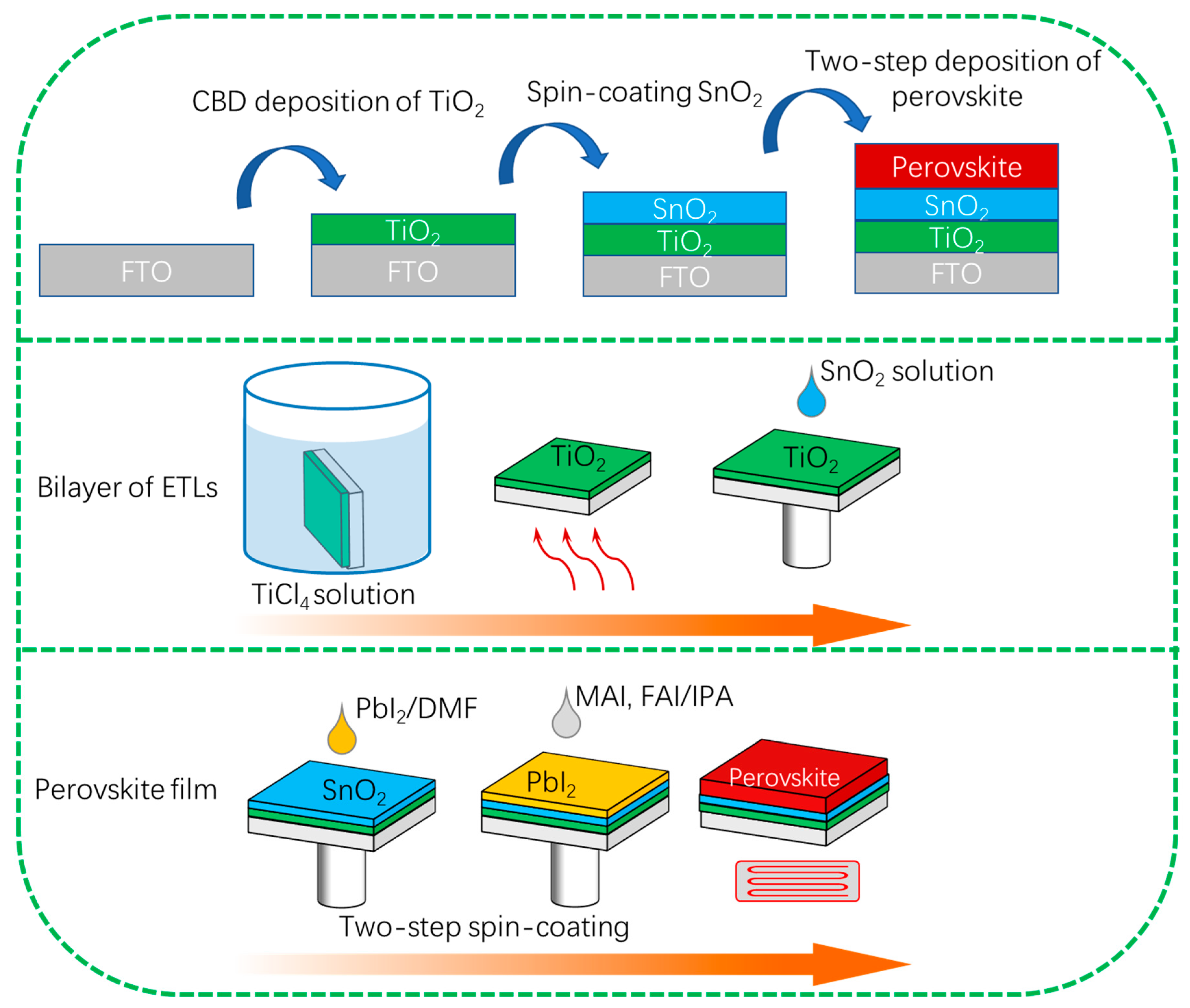
2. Materials and Methods

Materials: All reagents were used as received without further purification. Methylammonium iodide (MAI), methylammonium bromide (MABr), methylammonium chloride (MACl), formamidinium iodide (FAI), lead(II) iodide (PbI2) and 2,2′,7,7′-tetrakis(N,N-di-p-methoxyphenylamine)9,9′-spirobifluorene (Spiro-OMeTAD) (99.5%) were purchased from Xi’an Polymer Light Technology (Xi’an, China). Dimethylformamide (DMF), dimethyl sulfoxide (DMSO), isopropanol (IPA), chlorobenzene (CB), and titanium tetrachloride (TiCl4) were purchased from Sigma-Aldrich (Milwaukee, Germany).
Device Fabrication: The cleaned fluorine-doped tin oxide (FTO) substrates are treated using UV-ozone for 60 min. Then, the TiO2 thin layer was prepared by using the CBD method and the SnO2 thin layer was fabricated with spin-coating technologies, as shown in Figure 1. First, 2 M aqueous TiCl4 mother solution was prepared by dropping TiCl4 into distilled water. During the preparation, the mother solution was continuously stirred at a low temperature of around 0 °C. The as-prepared TiCl4 mother solution was stored in the refrigerator (<10 °C). Second, the as-prepared TiCl4 mother solution was diluted to a 0.2 M TiCl4 solution. The cleaned FTO substrates were placed vertically in the glassware. Then, 300 mL of 0.2 M TiCl4 solution was poured into the glassware. The glassware was put into an oven with a temperature of 75 °C. After 1 h heating, the glassware was taken out followed by rinsing the FTO substrates several times using distilled water. Finally, the FTO substrates were annealed at a high temperature of 450 °C for 30 min. The FTO substrates were washed by the acetone, distilled water, and ethyl alcohol for 20 min, respectively. Before the deposition of TiO2 thin films, the FTO substrates are treated by using UV-ozone for 60 min. SnO2 films were prepared by spin-coating Alfa Aesar SnO2 (diluted by H2O to 3%) at a speed of 3500 rpm for 30 s. The perovskite films were deposited by a two-step spin-coating method. Specifically, 1.35 M PbI2 and 0.0675 M CsI were dissolved in organic solvent (DMF/DMSO = 19:1). The PbI2 precursor solution was stirred at a temperature of 70 °C for 60 min. The mixed MAFA based organic cation precursor solution was prepared by dissolving 200 mg FAI, 100 mg MAI, 25 mg MABr and 25 mg MACl dissolved in 5 mL isopropanol. The PbI2 precursor solution was first spin-coated at a speed of 3000 rpm for 30 s. The MA/FA cation solution was spin-coated at 3000 rpm for 30s. After annealing at 150 °C for 10 min, the perovskite film of Cs0.05FA0.54MA0.41Pb(I0.98Br0.02)3 was obtained. The hole transport layer of the spiro-OMeTAD film was deposited by spin-coating the spiro-OMeTAD solution at a speed of 3500 rpm for 25 s. Finally, 80 nm Au film was deposited as a counter electrode by thermal evaporation.
Device Characterization: The diffraction data of perovskites are collected by using a Bruker D8 Discover diffractometer (Bruker AXS) from 10° to 60°. Surface and cross-section morphology images are recorded by a scanning electron microscope (SEM) (Helios NanoLab G3). The TRPL results were collected by using the Hamamatsu equipment which can provide an excitation wavelength of 450 nm. The photoluminescence (PL) spectra were acquired by a JASCO FP-8500 spectrometer with an excitation wavelength of 450 nm. The current-voltage (J-V) measurements were performed under one sun illumination (AM1.5G, 100 mW/cm2) by using a Keithley 2420. The devices were test by using a metal shadow mask with a dimension of 0.3 × 0.3 cm2. The EQE spectra of the devices were characterized by using Oriel IQE 200 equipment.

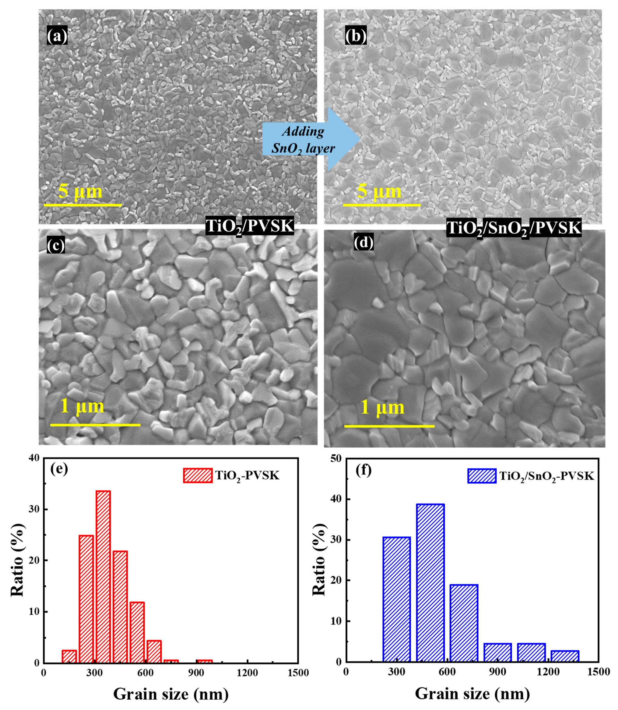
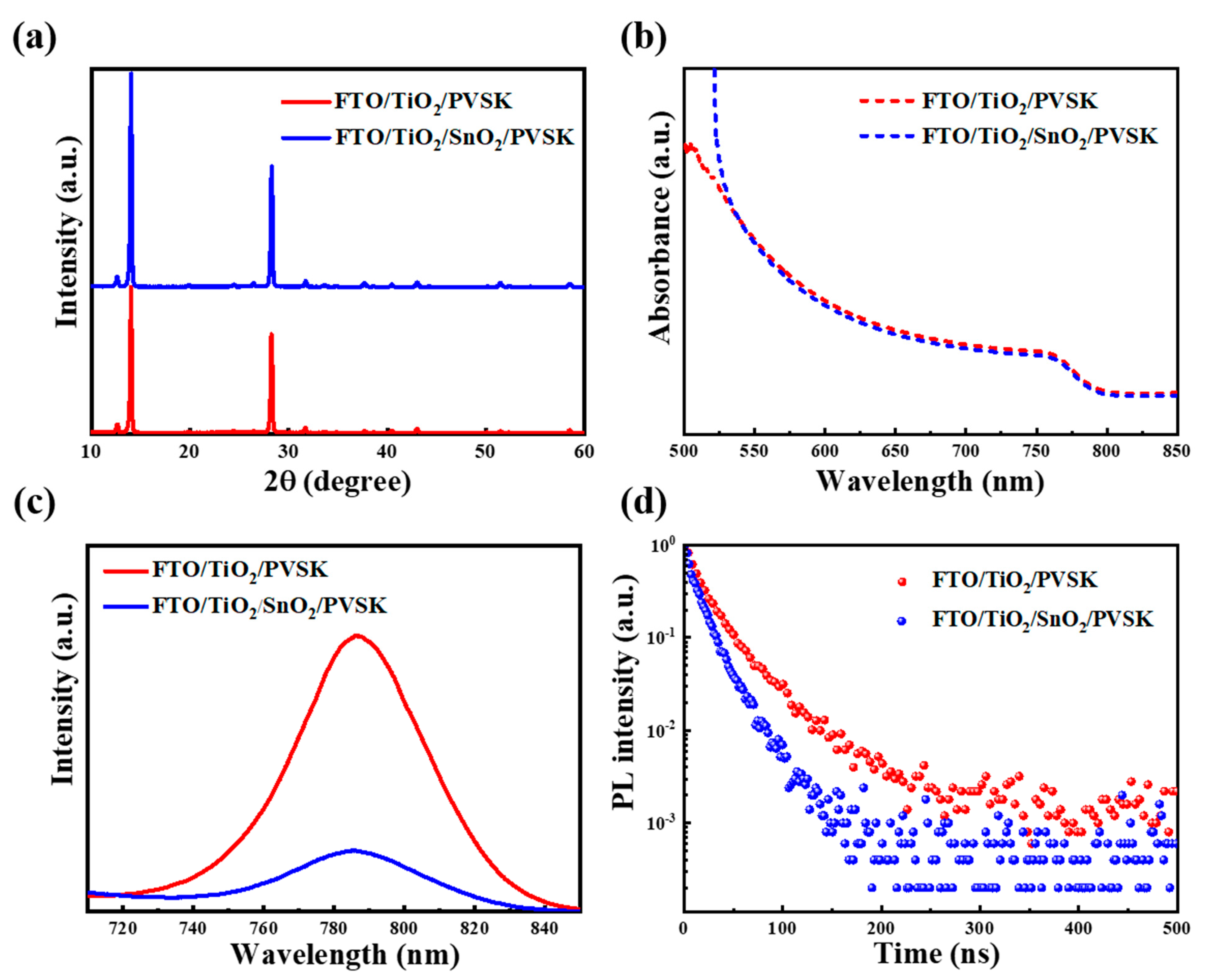
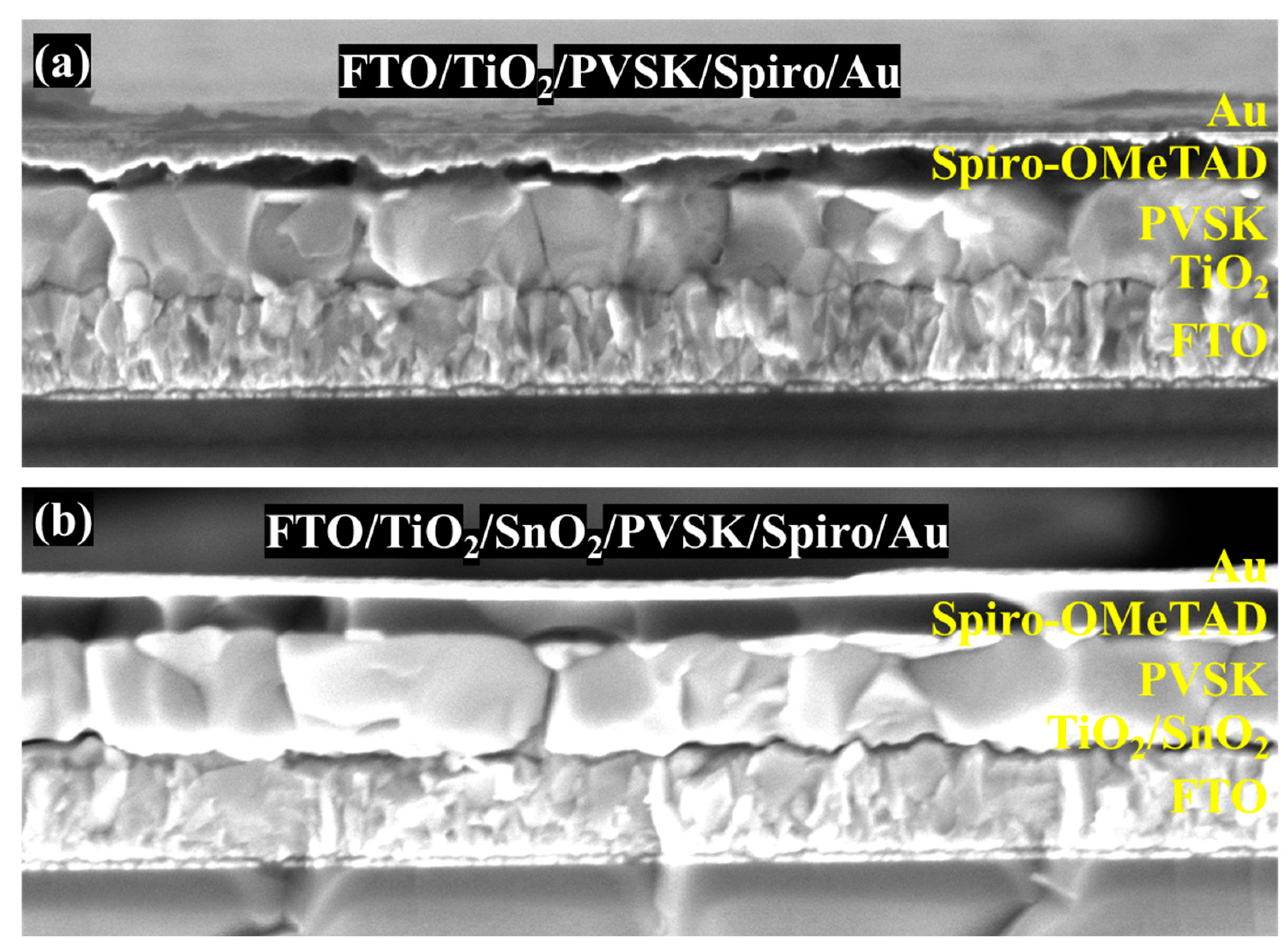
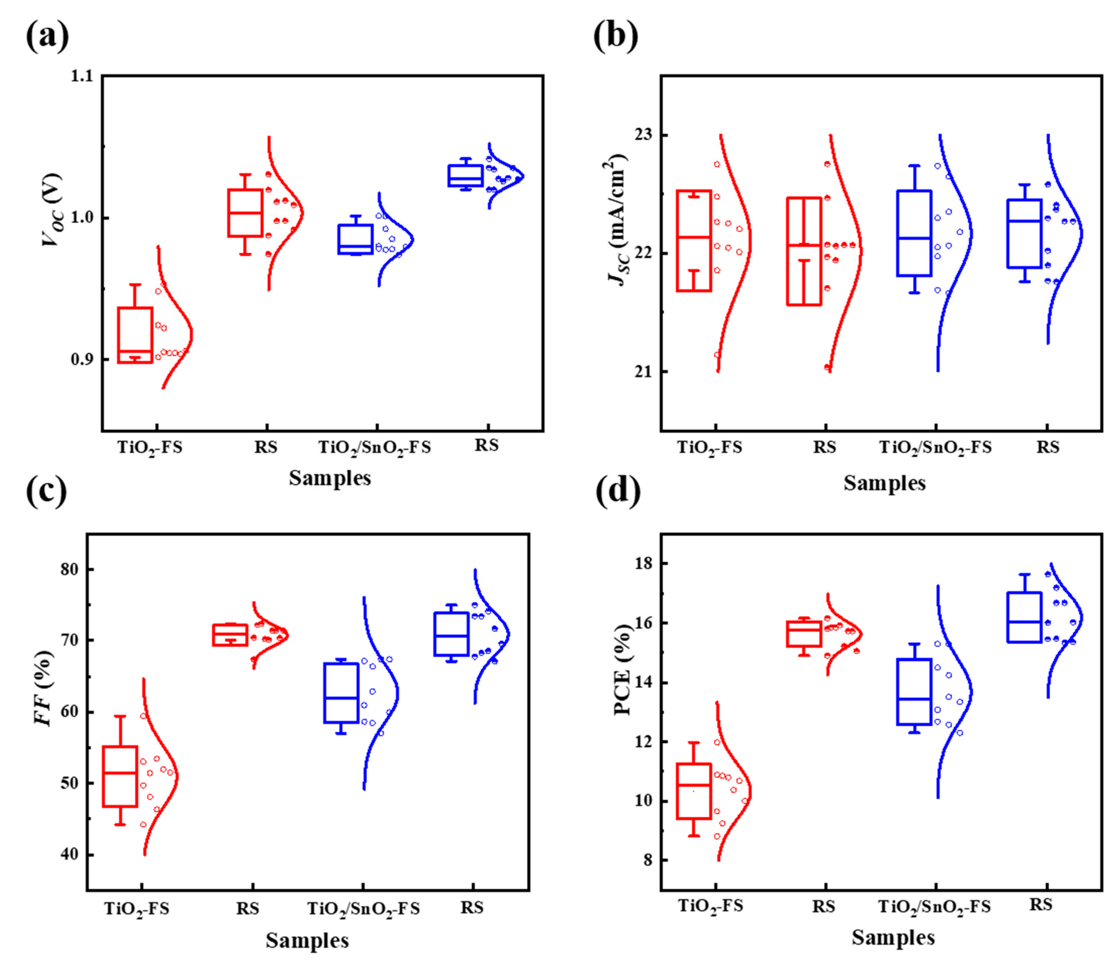
3. Results and Discussion

Figure 2a–d shows the top-view SEM images of the perovskite films fabricated on the TiO2 and TiO2/SnO2 substrates, which clearly shows a larger grain size of perovskite thin film based on the TiO2/SnO2 substrates, compared with that on the TiO2 substrates, with an average value changing from ~380 nm to ~540 nm, which can be verified by the statistics of perovskite grain size based on the TiO2 and TiO2/SnO2 substrates, as presented in Figure 2e,f. As is well-known, the commercial SnO2 colloid precursor is stabilized by incorporating potassium hydroxide (KOH) [24]. The presence of K ion in the SnO2 will diffuse into the perovskite thin film during the annealing process, which greatly enhances the crystallinity of perovskite grains, and reduces the hysteresis of resultant devices [25,26,27].
Furthermore, the phase structure of perovskite thin film deposited on the TiO2 and TiO2/SnO2 substrates was investigated by X-ray diffraction (XRD), as presented in Figure 3a. The increase of XRD intensity (on the TiO2/SnO2 substrate) verifies that the improved crystallinity of perovskites is accomplished with high absorption in a short-wavelength region (as shown in Figure 3b).
In addition, the steady-state photoluminescence (PL) and time-resolved photoluminescence (TRPL) experiments were carried out to investigate carrier transport behavior. As seen in Figure 3c,d, the faster PL quenching of the perovskite thin film on the TiO2/SnO2 substrate indicates an enhanced electron extraction capability [28]. Moreover, the lifetimes of the corresponding perovskite thin films were fitted by a biexponential decay function [29,30]. The lifetime of the TiO2/SnO2-based sample is 15.4 ns, which is shorter than that of the TiO2-based sample (22.2 ns), indicating a faster carrier extraction from the perovskite thin film to TiO2/SnO2 electron transport layer [31].
Figure 4a,b shows the cross-section SEM images of devices fabricated on TiO2 and TiO2/SnO2 substrates. The uniform and dense perovskite absorber layers not only ensure the light harvest, but also effectively impede the carrier recombination in the devices. The current density-voltage (J-V) curves of the devices were measured under standard AM 1.5 G illumination and are shown in Figure 5a and Table 1, while the key performance parameters of open-circuit voltage (VOC), short-circuit current (JSC), fill factor (FF), power conversion efficiency (PCE) and their statistical analyses are displayed in Figure 6a–d and Table 2, respectively. The PCE of 16.16% (VOC = 1.012 V, JSC = 22.06 mA/cm2 and FF = 72.4%) and 10.37% (VOC = 0.905 V, JSC = 22.06 mA/cm2 and FF = 51.9%) under reverse scan (RS) and forward scan (FS) indicate large hysteresis in the TiO2-based devices. In contrast, the high PCE of 17.64% (VOC = 1.041 V, JSC = 22.58 mA/cm2 and FF = 75.0%) and 15.29% (VOC = 1.001 V, JSC = 22.73 mA/cm2 and FF = 67.2%) under RS and FS were obtained for TiO2/SnO2-based solar cells. The improved efficiency of TiO2/SnO2-based solar cells can be attributed to a higher crystallinity of perovskite grains, which enhances light capture and reduces the defects at grain boundaries [14,25]. The EQE spectra of the corresponding devices were presented in Figure 5b. The improved EQE in the short wavelength in terms of TiO2/SnO2-based device indicates faster carrier extraction and reduced recombination at the TiO2/SnO2/PVSK interface [32]. Similarly, the enhanced EQE at the long wavelength region also suggests that reduced defects and carrier recombination in the perovskite bulk film, which can be explained by the enlarged grain size and improved crystallinity of the perovskite grains [32]. As a result, the integrated JSC from EQE of the TiO2/SnO2-based device is 21.59 mA/cm2, which is higher than that of the TiO2 based device (21.17 mA/cm2). Furthermore, the TiO2/SnO2-based device exhibited a stable output (under initial maximum power point (MPP) voltage) with a PCE of 17.65%. In contrast, the TiO2 based solar cell shows a poor output under MPP, yielding a low PCE of 15.74% (Figure 5c). More importantly, the hysteresis (hysteresis index (HI) = PCERS/PCEFS) of the TiO2/SnO2-based devices is also reduced, compared to TiO2-based devices [32,33,34]. The HI of the TiO2-based PSC is 1.56, which is decreased to 1.15 by incorporating SnO2 into devices to construct the TiO2/SnO2 bilayer ETL. Compared to TiO2 based devices with a large hysteresis of 1.51, the improved efficiency and reduced HI of 1.18 for TiO2/SnO2-based PSCs indicates the bilayer ETL can improve the reproducible fabrication and the device performance.

4. Conclusions

In summary, we developed a bilayer electron transport layer by combining CBD-TiO2 and spin-coated SnO2 in the perovskite solar cells. The TiO2/SnO2 bilayer ETLs provide not only a compact electron transport layer, but also accelerate the carrier transport in the solar cells. Furthermore, the presence of K ion from SnO2 can greatly improve the crystallinity of perovskite thin film and significantly reduce the hysteresis of resultant devices. Compared with the TiO2-based solar cells, the TiO2/SnO2-based solar cells demonstrate a higher PCE of 17.64% and a lower hysteresis index. These results highlight the potential fabrication of the TiO2/SnO2 bilayer electron transport layers and will be a beneficial strategy to fabricate a high-quality perovskite thin film solar cell.

Author Contributions

Conceptualization, X.S. and L.L.; methodology, X.S. and F.W.; software, X.S.; validation, X.S. and S.S.; formal analysis, X.S. and F.W.; investigation, X.S. and L.L.; resources, X.S.; data curation, S.S.; writing—original draft preparation, X.S.; writing—review and editing, L.L. and S.S.; project administration, F.W.; funding acquisition, X.S. and F.W. All authors have read and agreed to the published version of the manuscript.

Funding

This research was funded by the High-level Scientific Research Foundation for the introduction of talent of Nanjing Vocational University of Industry Technology under Nos. YK20-03-03 and YK20-03-02. The 2021 High-end training of professional leaders of teachers in higher vocational colleges in Jiangsu Province under No. 2021GRGDYX009. The National Natural Science Foundation of China under No. 32101535. The Jiangsu Postdoctoral Research Foundation under No. 2021K112B. The National Natural Science Foundation of China under No. 62205144. The Qing Lan project of Jiangsu Universities under No. QL078.

Data Availability Statement

The data is available on reasonable request from the corresponding author.

Conflicts of Interest

The authors declare no conflict of interest. The funders had no role in the design of the study; in the collection, analyses, or interpretation of data; in the writing of the manuscript; or in the decision to publish the results.

References

  1. Huang, H.-H.; Liu, Q.-H.; Tsai, H.; Shrestha, S.; Su, L.-Y.; Chen, P.-T.; Chen, Y.-T.; Yang, T.-A.; Lu, H.; Chuang, C.-H.; et al. A Simple One-Step Method with Wide Processing Window for High-Quality Perovskite Mini-module Fabrication. Joule 2021, 5, 958–974. [Google Scholar] [CrossRef]
  2. Tong, G.; Li, H.; Li, D.; Zhu, Z.; Xu, E.; Li, G.; Yu, L.; Xu, J.; Jiang, Y. Dual-phase CsPbBr3-CsPb2Br5 Perovskite Thin Films via Vapour Deposition for High-performance Rigid and Flexible Photodetectors. Small 2018, 14, 1702523–1702530. [Google Scholar] [CrossRef]
  3. Chao, L.; Niu, T.; Gao, W.; Ran, C.; Song, L.; Chen, Y.; Huang, W. Solvent Engineering of the Precursor Solution toward Large-Area Production of Perovskite Solar Cells. Adv. Mater. 2021, 33, 2005410. [Google Scholar] [CrossRef] [PubMed]
  4. Yoo, J.; Seo, G.; Chua, M.; Park, T.; Lu, Y.; Rotermund, F.; Kim, Y.-K.; Moon, C.; Jeon, N.; Correa-Baena, J.-P.; et al. Efficient Perovskite Solar Cells via Improved Carrier Management. Nature 2021, 590, 587–593. [Google Scholar] [CrossRef]
  5. Yang, H.; Xu, E.; Wu, C.; Li, J.; Liu, B.; Hong, F.; Zhang, L.; Chang, Y.; Zhang, Y.; Tong, G.; et al. Bifunctional Interface Engineering by Oxidating Layered TiSe2 for High-Performance CsPbBr3 Solar Cells. ACS Appl. Energy Mater. 2022, 5, 8254–8261. [Google Scholar] [CrossRef]
  6. Tong, G.; Son, D.; Ono, L.; Liu, Y.; Hu, Y.; Zhang, H.; Jamshaid, A.; Qiu, L.; Liu, Z.; Qi, Y. Scalable Fabrication of >90 cm2 Perovskite Solar Modules with 1000 h Operational Stability Based on the Intermediate Phase Strategy. Adv. Energy Mater. 2021, 11, 2003712. [Google Scholar] [CrossRef]
  7. Werner, J.; Boyd, C.C.; Moot, T.; Wolf, E.J.; France, R.M.; Johnson, S.A.; van Hest, M.F.A.M.; Luther, J.M.; Zhu, K.; Berry, J.J.; et al. Learning from Existing Photovoltaic Technologies to Identify Alternative Perovskite Module Designs. Energy Environ. Sci. 2020, 13, 3393. [Google Scholar] [CrossRef]
  8. Liu, Z.; Qiu, L.; Ono, L.; He, S.; Hu, Z.; Jiang, M.; Tong, G.; Wu, Z.; Jiang, Y.; Son, D.-Y.; et al. A Holistic Approach to Interface Stabilization for Efficient Perovskite Solar Modules with over 2,000-hour Operational Stability. Nat. Energy 2020, 5, 596–604. [Google Scholar] [CrossRef]
  9. Wu, T.; Liu, X.; Luo, X.; Segawa, H.; Tong, G.; Zhang, Y.; Ono, L.K.; Qi, Y.B.; Han, L. Heterogeneous FASnI3 Absorber with Enhanced Electric Field for High-Performance Lead-Free Perovskite Solar Cells. Nano-Micro Lett. 2022, 14, 99. [Google Scholar] [CrossRef]
  10. Jeon, N.; Na, H.; Jung, E.; Yang, T.-Y.; Lee, Y.; Kim, G.; Shin, H.-W.; Seok, S.I.; Lee, J.; Seo, J. A Fluorene-Terminated Hole-transporting Material for Highly Efficient and Stable Perovskite Solar Cells. Nat. Energy 2018, 3, 682–689. [Google Scholar] [CrossRef]
  11. Lin, L.; Jones, T.; Wang, J.; Cook, A.; Pham, N.; Duffy, N.; Mihaylov, B.; Grigore, M.; Anderson, K.; Duck, B.; et al. Strategically Constructed Bilayer Tin (IV) Oxide as Electron Transport Layer Boosts Performance and Reduces Hysteresis in Perovskite Solar Cells. Small 2020, 16, 1901466. [Google Scholar] [CrossRef] [PubMed]
  12. Chen, T.; Tong, G.; Xu, E.; Li, H.; Li, P.; Zhu, Z.; Tang, J.; Qi, Y.B.; Jiang, Y. Accelerating Hole Extraction by Inserting 2D Ti3C2-MXene Interlayer to All Inorganic Perovskite Solar Cells with Long-Term Stability. J. Mater. Chem. A 2019, 7, 20597–20603. [Google Scholar] [CrossRef]
  13. Wu, W.-Q.; Chen, D.; Caruso, R.; Cheng, Y.-B. Recent Progress in Hybrid Perovskite Solar Cells Based on N-type Materials. J. Mater. Chem. A 2017, 5, 10092–10109. [Google Scholar] [CrossRef]
  14. Tong, G.; Ono, L.; Liu, Y.; Zhang, H.; Bu, T.; Qi, Y. Up-Scalable Fabrication of SnO2 with Multifunctional Interface for High Performance Perovskite Solar Modules. Nano-Micro Lett. 2021, 13, 155. [Google Scholar] [CrossRef]
  15. Paik, M.; Lee, Y.; Yun, H.; Lee, S.; Hong, S.; Seok, S. TiO2 Colloid-Spray Coated Electron-Transporting Layers for Efficient Perovskite Solar Cells. Adv. Energy Mater. 2020, 10, 2001799. [Google Scholar] [CrossRef]
  16. Li, H.; Tong, G.; Chen, T.; Zhu, H.; Li, G.; Chang, Y.; Wang, L.; Jiang, Y. Interface Engineering Using Perovskite Derivative-Phase for Efficient and Stable CsPbBr3-Solar Cells. J. Mater. Chem. A 2018, 6, 14225. [Google Scholar] [CrossRef]
  17. Wang, P.; Li, R.; Chen, B.; Hou, F.; Zhang, J.; Zhao, Y.; Zhang, X. Gradient Energy Alignment Engineering for Planar Perovskite Solar Cells with Efficiency Over 23%. Adv. Mater. 2020, 32, 1905766. [Google Scholar] [CrossRef] [PubMed]
  18. Wojciechowski, K.; Stranks, S.; Abate, A.; Sadoughi, G.; Sadhanala, A.; Kopidakis, N.; Rumbles, G.; Li, C.-Z.; Friend, R.; Jen, A.-Y.; et al. Heterojunction Modification for Highly Efficient Organic–Inorganic Perovskite Solar Cells. ACS Nano 2014, 8, 12701–12709. [Google Scholar] [CrossRef]
  19. Shin, S.; Yeom, E.; Yang, W.; Hur, S.; Kim, M.; Im, J.; Seo, J.; Noh, J.; Seok, S. Colloidally Prepared La-doped BaSnO3 Electrodes for Efficient, Photostable Perovskite Solar Cells. Science 2017, 356, 167–171. [Google Scholar] [CrossRef] [PubMed]
  20. Jiang, Q.; Zhang, X.; You, J. SnO2: A Wonderful Electron Transport Layer for Perovskite Solar Cells. Small 2018, 14, 1801154. [Google Scholar] [CrossRef]
  21. Jiang, Q.; Zhang, L.; Wang, H.; Yang, X.; Meng, J.; Liu, H.; Yin, Z.; Wu, J.; Zhang, X.; You, J. Enhanced Electron Extraction Using SnO2 for High-Efficiency Planar-Structure HC(NH2)2PbI3-Based Perovskite Solar Cells. Nat. Energy 2016, 2, 16177. [Google Scholar] [CrossRef]
  22. Deng, K.; Chen, Q.; Li, L. Modification Engineering in SnO2 Electron Transport Layer toward Perovskite Solar Cells: Efficiency and Stability. Adv. Funct. Mater. 2020, 30, 2004209. [Google Scholar] [CrossRef]
  23. Xu, X.; Zhang, H.; Shi, J.; Dong, J.; Luo, Y.; Li, D.; Meng, Q. Highly Efficient Planar Perovskite Solar Cells with a TiO2/ZnO Electron Transport Bilayer. J. Mater. Chem. A 2015, 3, 19288–19293. [Google Scholar] [CrossRef]
  24. Bu, T.; Li, J.; Zheng, F.; Chen, W.; Wen, X.; Ku, Z.; Peng, Y.; Zhong, J.; Cheng, Y.; Huang, F. Universal Passivation Strategy to Slot-Die Printed SnO2 for Hysteresis-Free Efficient Flexible Perovskite Solar Module. Nat. Commun. 2018, 9, 4609. [Google Scholar] [CrossRef] [Green Version]
  25. Zhu, P.; Gu, S.; Luo, X.; Gao, Y.; Li, S.; Zhu, J.; Tan, H. Simultaneous Contact and Grain-Boundary Passivation in Planar Perovskite Solar Cells Using SnO2-KCl Composite Electron Transport Layer. Adv. Energy Mater. 2019, 10, 1903083. [Google Scholar] [CrossRef]
  26. Bu, T.; Li, J.; Li, H.; Tian, C.; Su, J.; Tong, G.; Ono, L.K.; Wang, C.; Lin, Z.; Chai, N.; et al. Lead Halide-Templated Crystallization of Methylamine-Free Perovskite for Efficient Photovoltaic Modules. Science 2021, 378, 1327–1332. [Google Scholar] [CrossRef] [PubMed]
  27. Bi, H.; Liu, B.; He, D.; Bai, L.; Wang, W.; Zang, Z.; Chen, J. Interfacial Defect Passivation and Stress Release by Multifunctional KPF6 Modification for Planar Perovskite Solar Cells with Enhanced Efficiency and Stability. Chem. Eng. J. 2021, 418, 129375. [Google Scholar] [CrossRef]
  28. Liu, Z.; Deng, K.; Hu, J.; Li, L. Coagulated SnO2 Colloids for High-Performance Planar Perovskite Solar Cells with Negligible Hysteresis and Improved Stability. Angew. Chem. 2019, 58, 11497–11504. [Google Scholar] [CrossRef]
  29. Tong, G.; Jiang, M.; Son, D.; Ono, L.; Qi, Y. 2D Derivative Phase Induced Growth of 3D All Inorganic Perovskite Micro–Nanowire Array Based Photodetectors. Adv. Funct. Mater. 2020, 30, 2002526. [Google Scholar] [CrossRef]
  30. Tong, G.; Chen, T.; Li, H.; Qiu, L.; Liu, Z.; Dang, Y.; Song, W.; Ono, L.K.; Jiang, Y.; Qi, Y.B. Phase Transition Induced Recrystallization and Low Surface Potential Barrier Leading to 10.91%-Efficient CsPbBr3 Perovskite Solar Cells. Nano Energy 2018, 65, 536–542. [Google Scholar] [CrossRef]
  31. Wang, Z.; Wu, T.; Xiao, L.; Qin, P.; Yu, X.; Ma, L.; Xiong, L.; Li, H.; Chen, X.; Wang, Z.; et al. Multifunctional Potassium Hexafluorophosphate Passivate Interface Defects for High Efficiency Perovskite Solar Cells. Power Sources 2021, 488, 229451. [Google Scholar] [CrossRef]
  32. Tong, G.; Son, D.-Y.; Ono, L.; Kang, H.-B.; He, S.; Qiu, L.; Zhang, H.; Liu, Y.; Hieulle, J.; Qi, Y. Removal of Residual Compositions by Powder Engineering for High Efficiency Formamidinium-Based Perovskite Solar Cells with Operation Lifetime over 2000 h. Nano Energy 2021, 87, 106152. [Google Scholar] [CrossRef]
  33. Domanski, K.; Alharbi, E.; Hagfeldt, A.; Grätzel, M.; Tress, W. Systematic Investigation of the Impact of Operation Conditions on the Degradation Behaviour of Perovskite Solar Cells. Nat. Energy 2018, 3, 61–67. [Google Scholar] [CrossRef]
  34. Habisreutinger, S.; Noel, N.; Snaith, H. Hysteresis Index: A Figure without Merit for Quantifying Hysteresis in Perovskite Solar Cells. ACS Energy Lett. 2018, 3, 2472–2476. [Google Scholar] [CrossRef]
Figure 1. Schematic illustration of the bilayer of ETLs (TiO2 and SnO2 films) and perovskite films fabricated by chemical bath deposition and spin-coating.
Nanomaterials 13 00249 g001
Figure 2. (a) Top-view SEM images of monolayer TiO2-ETL PSCs and bilayer TiO2/SnO2-ETL PSCs (ad), and their corresponding statistic of grain size (e,f).
Nanomaterials 13 00249 g002
Figure 3. (a) XRD patterns, (b) absorption spectra, (c) PL spectra and (d) TRPL curves of the perovskite films deposited on FTO/TiO2 and FTO/TiO2/SnO2 substrates.
Nanomaterials 13 00249 g003
Figure 4. Cross-section images of PSCs in (a) TiO2-PSCs and (b) TiO2/SnO2 PSCs.
Nanomaterials 13 00249 g004
Figure 5. (a) Measured current density-voltage curves of champion devices. (b) Corresponding EQE spectra and their integrated current density. (c) Stable output of perovskite solar cells based on based on TiO2 and TiO2/SnO2 ETLs.
Nanomaterials 13 00249 g005
Figure 6. Statistical distribution of TiO2 and TiO2/SnO2 based PSCs (10 devices). (a) VOC, (b) JSC, (c) FF and (d) PCE.
Nanomaterials 13 00249 g006
Table 1. Photovoltaics parameters of PSCs based on TiO2 and TiO2/SnO2 ETLs.
SampleScan DirectionVoc (V)Jsc (mA/cm2)FF PCE (%)HI
TiO2/SnO2 PSCFS.1.00122.730.67215.291.18
RS.1.04122.580.75017.64
TiO2-PSCsFS.0.90522.060.51910.371.51
RS.1.01222.060.72416.16
Table 2. Average photovoltaics parameters of PSCs based on TiO2 and TiO2/SnO2 ETLs.
SampleScan DirectionVoc (V)Jsc (mA/cm2)FFPCE (%)
TiO2/SnO2 PSCFS.0.985 ± 0.01022.17 ± 0.340.626 ± 0.03913.68 ± 1.04
RS.1.029 ± 0.00722.16 ± 0.270.709 ± 0.02816.18 ± 0.78
TiO2-PSCsFS.0.917 ± 0.01822.11 ± 0.400.5090 ± 0.04010.33 ± 0.88
RS.1.003 ± 0.01622.01 ± 0.430.707 ± 0.01415.61 ± 0.40
Disclaimer/Publisher’s Note: The statements, opinions and data contained in all publications are solely those of the individual author(s) and contributor(s) and not of MDPI and/or the editor(s). MDPI and/or the editor(s) disclaim responsibility for any injury to people or property resulting from any ideas, methods, instructions or products referred to in the content.

