
Rapid Production of Carbon Nanotube Film for Bioelectronic Applications

Abstract
:1. Introduction
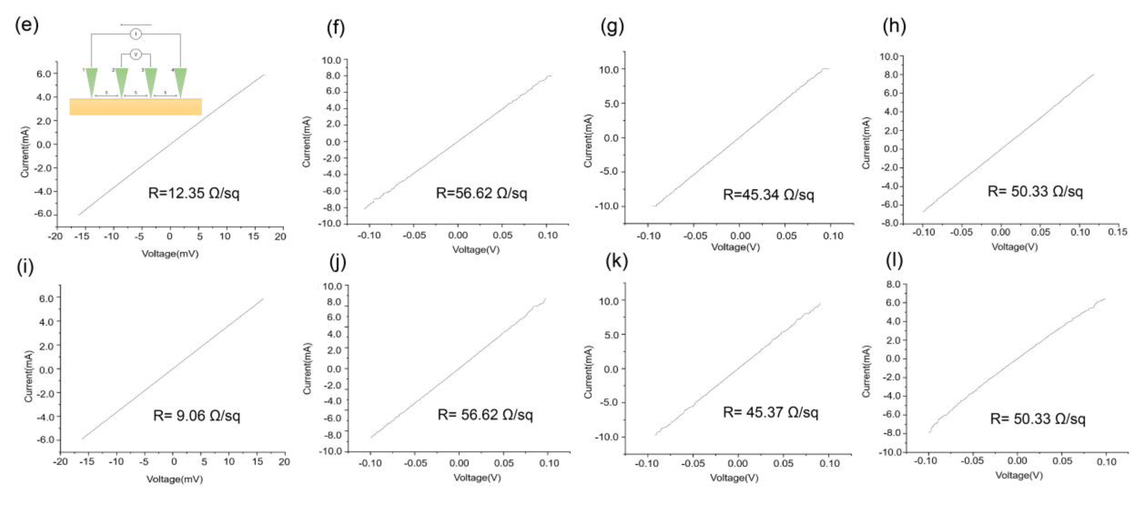
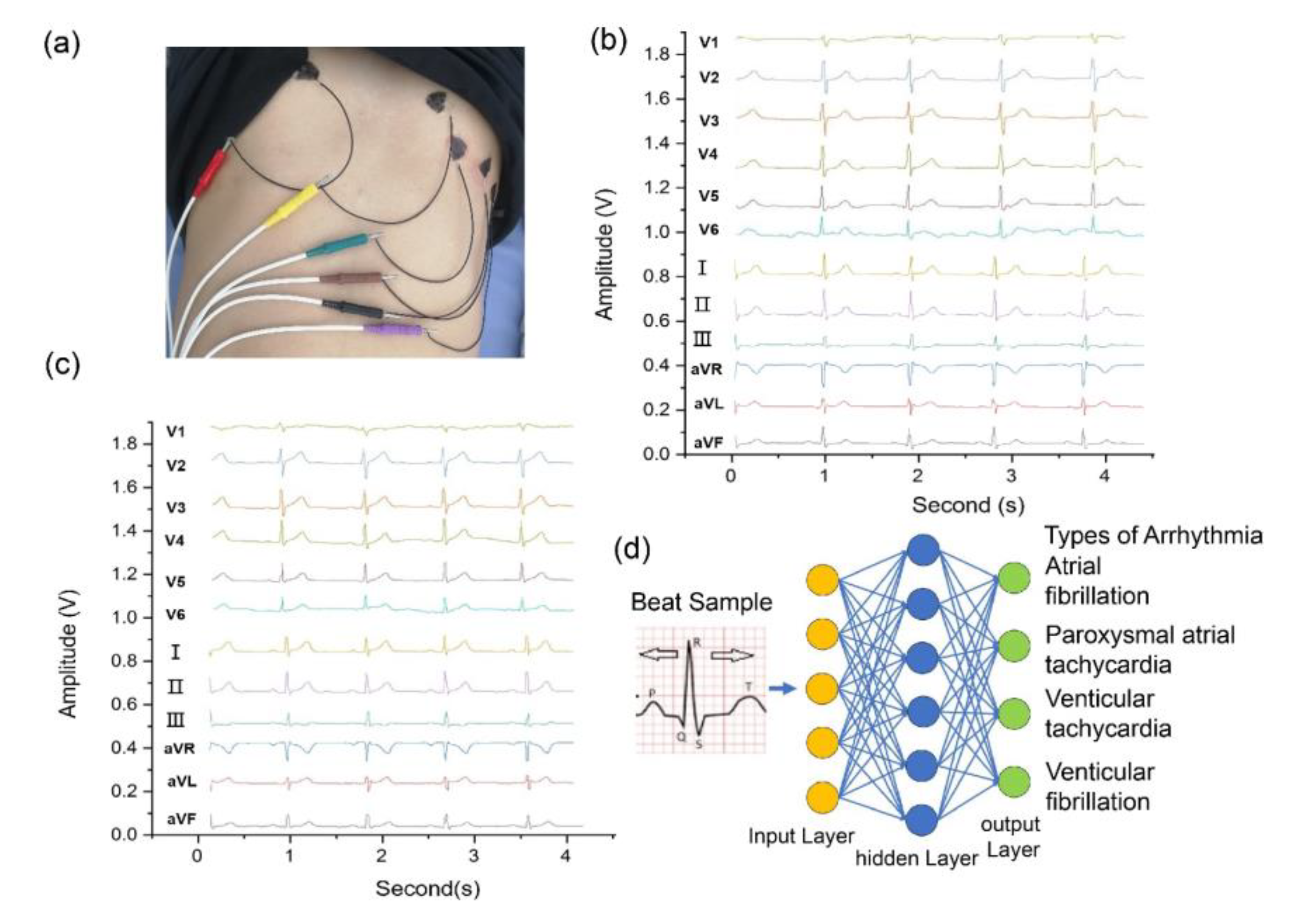
2. Results and Discussion
3. Method
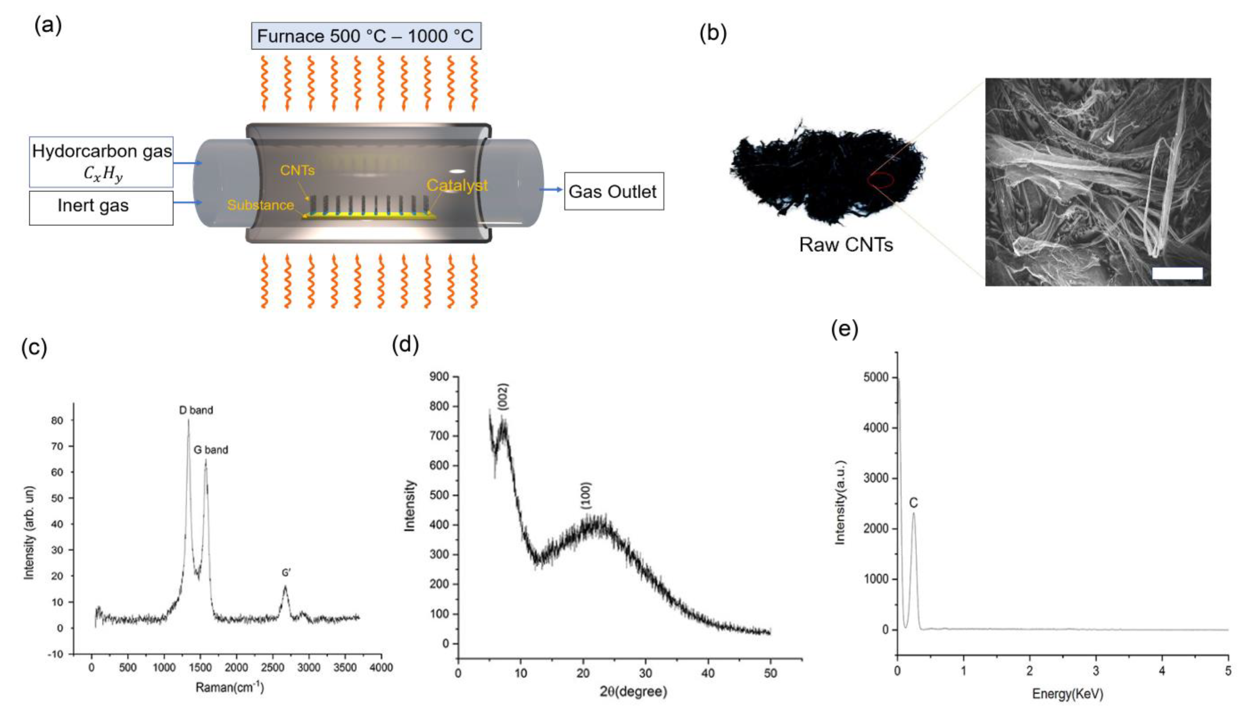
3.1. CNT Synthesis
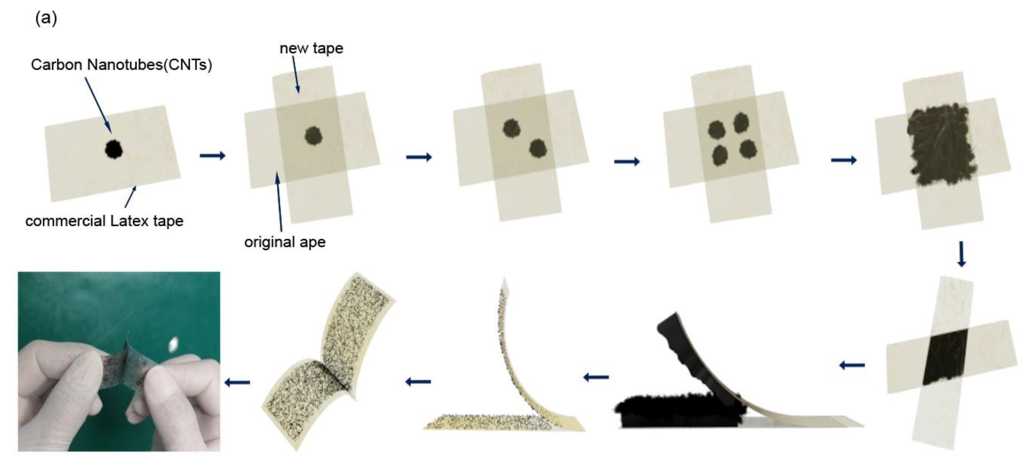
3.2. Conductive Tape Fabrication
3.3. Electrical Characterization
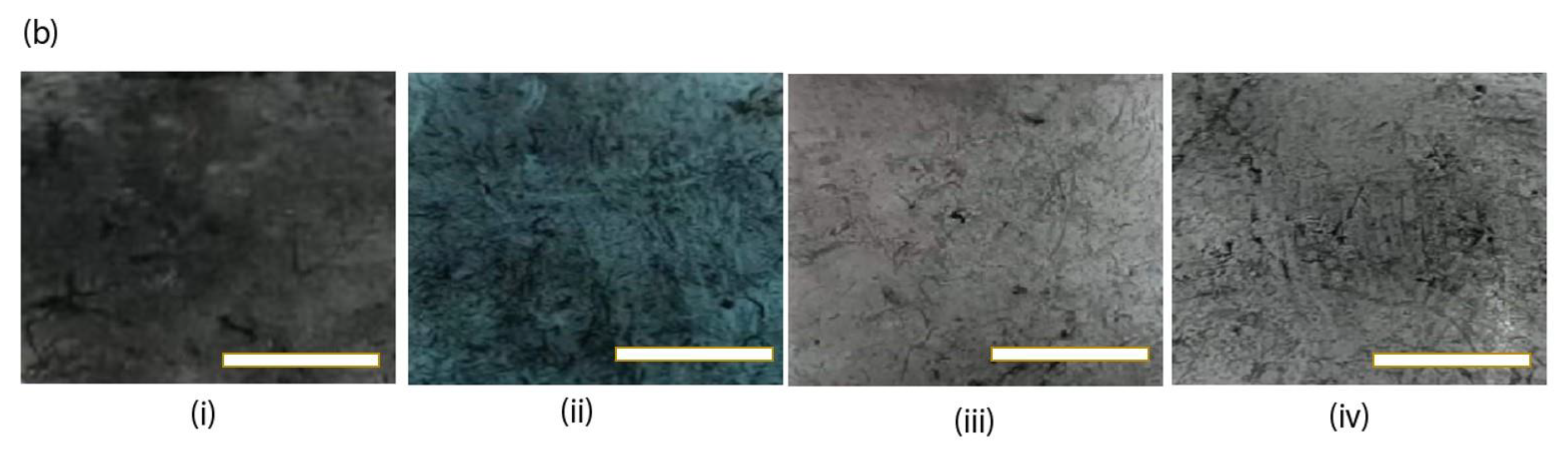
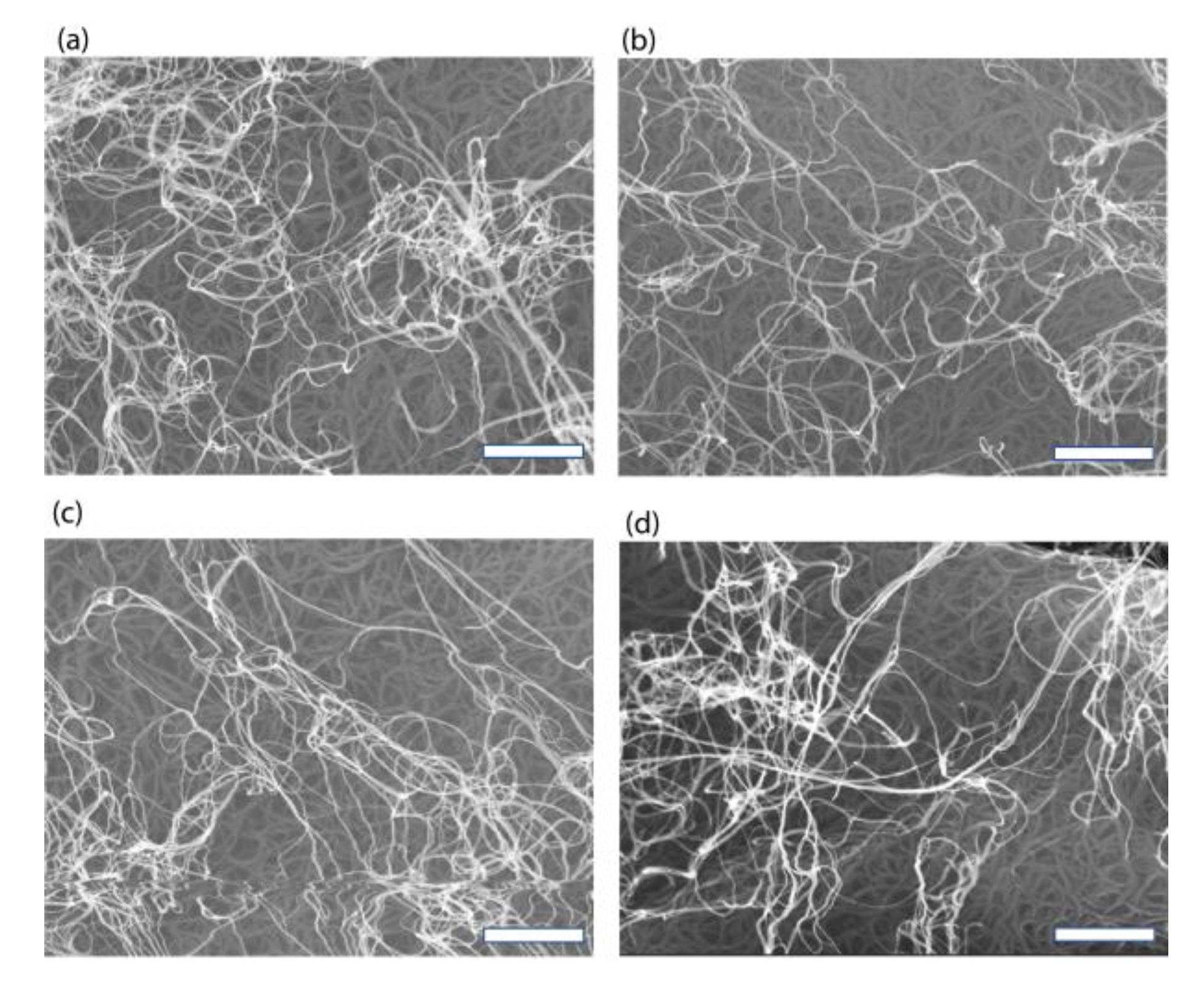
3.4. Morphology Characterization
3.5. Raman Spectroscopy, X-ray Diffraction, EDS Analysis and TEM Morphology
3.6. Electrocardiogram Measurement
4. Conclusions
Author Contributions
Funding
Institutional Review Board Statement
Informed Consent Statement
Acknowledgments
Conflicts of Interest
References
- Gates, B.D. Flexible electronics. Science 2009, 323, 1566–1567. [Google Scholar] [CrossRef] [PubMed]
- MacDonald, W.A.; Electronics, F. Latest advances in substrates for flexible electronics. Large Area Flex. Electron. 2015, 291–314. [Google Scholar]
- Nathan, A.; Ahnood, A.; Cole, M.T.; Lee, S.; Suzuki, Y.; Hiralal, P.; Bonaccorso, F.; Hasan, T.; Garcia-Gancedo, L.; Dyadyusha, A.; et al. Flexible electronics: The next ubiquitous platform. Proc. IEEE 100 2012, 100, 1486–1517. [Google Scholar] [CrossRef]
- Wong, W.S.; Chabinyc, M.L.; Ng, T.-N.; Salleo, A. Applications. Materials and novel patterning methods for flexible electronics. Flex. Electron. Mater. Appl. 2009, 11, 143–181. [Google Scholar]
- Choi, C.; Lee, J.A.; Choi, A.Y.; Kim, Y.T.; Lepró, X.; Lima, M.D.; Baughman, R.H.; Kim, S.J. Flexible supercapacitor made of carbon nanotube yarn with internal pores. Adv. Mater. 2014, 26, 2059–2065. [Google Scholar] [CrossRef] [PubMed]
- Gong, M.; Zhang, L.; Wan, P. Polymer nanocomposite meshes for flexible electronic devices. Prog. Polym. Sci. 2020, 107, 101279. [Google Scholar] [CrossRef]
- Pu, X.; Liu, M.; Chen, X.; Sun, J.; Du, C.; Zhang, Y.; Zhai, J.; Hu, W.; Wang, Z.L. Ultrastretchable, transparent triboelectric nanogenerator as electronic skin for biomechanical energy harvesting and tactile sensing. Sci. Adv. 2017, 3, e1700015. [Google Scholar] [CrossRef]
- Wu, M.; Yao, K.; Li, D.; Huang, X.; Liu, Y.; Wang, L.; Song, E.; Yu, J.; Yu, X. Self-powered skin electronics for energy harvesting and healthcare monitoring. Mater. Today Energy 2021, 21, 100786. [Google Scholar] [CrossRef]
- Aydın, E.B.; Sezgintürk, M.K. Indium tin oxide (ITO): A promising material in biosensing technology. TrAC Trends Anal. Chem. 2017, 97, 309–315. [Google Scholar] [CrossRef]
- Chen, S.F.; Deng, Y.; Xiong, H.; Lei, H.C. Research status of recovery of indium from indium-tin oxide (ITO) targets. In Materials Science Forum; Trans Tech Publications Ltd.: Zürich, Switzerland, 2019; pp. 1259–1264. [Google Scholar]
- Hayden, O.; Agarwal, R.; Lu, W. Semiconductor nanowire devices. Nano Today 2008, 3, 12–22. [Google Scholar] [CrossRef]
- Kim, D.H.; Xiao, J.; Song, J.; Huang, Y.; Rogers, J.A. Stretchable, curvilinear electronics based on inorganic materials. Adv. Mater. 2010, 22, 2108–2124. [Google Scholar] [CrossRef] [PubMed]
- Rogers, J.A.; Someya, T.; Huang, Y. Materials and mechanics for stretchable electronics. Science 2010, 327, 1603–1607. [Google Scholar] [CrossRef] [PubMed] [Green Version]
- Jang, H.; Park, Y.J.; Chen, X.; Das, T.; Kim, M.S.; Ahn, J.H. Graphene-based flexible and stretchable electronics. Adv. Mater. 2016, 28, 4184–4202. [Google Scholar] [CrossRef] [PubMed]
- Yoon, J.; Park, W.; Bae, G.Y.; Kim, Y.; Jang, H.S.; Hyun, Y.; Lim, S.K.; Kahng, Y.H.; Hong, W.K.; Lee, B.H.; et al. Flexible Electronics: Highly Flexible and Transparent Multilayer MoS2 Transistors with Graphene Electrodes. Small 2013, 9, 3185. [Google Scholar] [CrossRef]
- Arthur, D.; Glatkowski, P.; Wallis, P.; Trottier, M. P-86: Flexible Transparent Circuits from Carbon Nanotubes. In SID Symposium Digest of Technical Papers; Blackwell Publishing Ltd.: Oxford, UK, 2004; pp. 582–585. [Google Scholar]
- Hu, L.; Choi, J.W.; Yang, Y.; Jeong, S.; La Mantia, F.; Cui, L.-F.; Cui, Y. Highly conductive paper for energy-storage devices. Proc. Natl. Acad. Sci. USA 2009, 106, 21490–21494. [Google Scholar] [CrossRef] [PubMed] [Green Version]
- Majumder, M.; Rendall, C.; Li, M.; Behabtu, N.; Eukel, J.A.; Hauge, R.H.; Schmidt, H.K.; Pasquali, M. Insights into the physics of spray coating of SWNT films. Chem. Eng. Sci. 2010, 65, 2000–2008. [Google Scholar] [CrossRef]
- Show, Y.; Itabashi, H. Electrically conductive material made from CNT and PTFE. Diam. Relat. Mater. 2008, 17, 602–605. [Google Scholar] [CrossRef]
- Susi, T.; Kaskela, A.; Zhu, Z.; Ayala, P.; Arenal, R.; Tian, Y.; Laiho, P.; Mali, J.; Nasibulin, A.G.; Jiang, H.; et al. Nitrogen-doped single-walled carbon nanotube thin films exhibiting anomalous sheet resistances. Chem. Mater. 2011, 23, 2201–2208. [Google Scholar] [CrossRef]
- Tang, H.; Chen, J.; Yao, S.; Nie, L.; Kuang, Y.; Huang, Z.; Wang, D.; Ren, Z. Deposition and electrocatalytic properties of platinum on well-aligned carbon nanotube (CNT) arrays for methanol oxidation. Mater. Chem. Phys. 2005, 92, 548–553. [Google Scholar] [CrossRef]
- Tzeng, Y.; Chen, Y.; Liu, C. Electrical contacts between carbon-nanotube coated electrodes. Diam. Relat. Mater. 2003, 12, 774–779. [Google Scholar] [CrossRef]
- Wang, Y.; Liu, H.; Sun, X.; Zhitomirsky, I. Manganese dioxide–carbon nanotube nanocomposites for electrodes of electrochemical supercapacitors. Scr. Mater. 2009, 61, 1079–1082. [Google Scholar] [CrossRef]
- Williams, Q.L.; Liu, X.; Walters, W., Jr.; Zhou, J.-G.; Edwards, T.Y.; Smith, F.L.; Williams, G.E.; Mosley, B.L. Boron-doped carbon nanotube coating for transparent, conducting, flexible photonic devices. Appl. Phys. Lett. 2007, 91, 143116. [Google Scholar] [CrossRef] [Green Version]
- Xiao, G.; Tao, Y.; Lu, J.; Zhang, Z. Highly conductive and transparent carbon nanotube composite thin films deposited on polyethylene terephthalate solution dipping. Thin Solid Film. 2010, 518, 2822–2824. [Google Scholar] [CrossRef] [Green Version]
- Dürkop, T.; Getty, S.A.; Cobas, E.; Fuhrer, M.S. Extraordinary mobility in semiconducting carbon nanotubes. Nano Lett. 2004, 4, 35–39. [Google Scholar] [CrossRef]
- Treacy, M.J.; Ebbesen, T.W.; Gibson, J.M. Exceptionally high Young’s modulus observed for individual carbon nanotubes. Nature 1996, 381, 678–680. [Google Scholar] [CrossRef]
- Pop, E.; Mann, D.; Wang, Q.; Goodson, K.; Dai, H. Thermal conductance of an individual single-wall carbon nanotube above room temperature. Nano Lett. 2006, 6, 96–100. [Google Scholar] [CrossRef] [Green Version]
- Peng, B.; Locascio, M.; Zapol, P.; Li, S.; Mielke, S.L.; Schatz, G.C.; Espinosa, H.D. Measurements of near-ultimate strength for multiwalled carbon nanotubes and irradiation-induced crosslinking improvements. Nat. Nanotechnol. 2008, 3, 626–631. [Google Scholar] [CrossRef]
- Sun, D.-M.; Timmermans, M.Y.; Tian, Y.; Nasibulin, A.G.; Kauppinen, E.I.; Kishimoto, S.; Mizutani, T.; Ohno, Y. Flexible high-performance carbon nanotube integrated circuits. Nat. Nanotechnol. 2011, 6, 156–161. [Google Scholar] [CrossRef]
- Hecht, D.S.; Heintz, A.M.; Lee, R.; Hu, L.; Moore, B.; Cucksey, C.; Risser, S. High conductivity transparent carbon nanotube films deposited from superacid. Nanotechnology 2011, 22, 075201. [Google Scholar] [CrossRef]
- Yanagi, K.; Miyata, Y.; Kataura, H. Optical and conductive characteristics of metallic single-wall carbon nanotubes with three basic colors; cyan, magenta, and yellow. Appl. Phys. Express 2008, 1, 034003. [Google Scholar] [CrossRef]
- Fagan, J.A.; Becker, M.L.; Chun, J.; Nie, P.; Bauer, B.J.; Simpson, J.R.; Hight-Walker, A.; Hobbie, E.K. Centrifugal length separation of carbon nanotubes. Langmuir 2008, 24, 13880–13889. [Google Scholar] [CrossRef] [PubMed]
- Chi, Y.M.; Jung, T.-P.; Cauwenberghs, G. Dry-contact and noncontact biopotential electrodes: Methodological review. IEEE Rev. Biomed. Eng. 2010, 3, 106–119. [Google Scholar] [CrossRef] [PubMed] [Green Version]
- Lee, S.M.; Byeon, H.J.; Lee, J.H.; Baek, D.H.; Lee, K.H.; Hong, J.S.; Lee, S.-H. Self-adhesive epidermal carbon nanotube electronics for tether-free long-term continuous recording of biosignals. Sci. Rep. 2014, 4, 6074. [Google Scholar] [CrossRef] [PubMed] [Green Version]
- Miao, F.; Cheng, Y.; He, Y.; He, Q.; Li, Y. A wearable context-aware ECG monitoring system integrated with built-in kinematic sensors of the smartphone. Sensors 2015, 15, 11465–11484. [Google Scholar] [CrossRef] [Green Version]
- Searle, A.; Kirkup, L. A direct comparison of wet, dry and insulating bioelectric recording electrodes. Physiol. Meas. 2000, 21, 271. [Google Scholar] [CrossRef] [PubMed]
- Pantelopoulos, A.; Bourbakis, N.G. A survey on wearable sensor-based systems for health monitoring and prognosis. IEEE Trans. Syst. Man Cybern. Part C 2009, 40, 1–12. [Google Scholar] [CrossRef] [Green Version]
- Meziane, N.; Webster, J.; Attari, M.; Nimunkar, A. Dry electrodes for electrocardiography. Physiol. Meas. 2013, 34, R47. [Google Scholar] [CrossRef]
- Baek, J.-Y.; An, J.-H.; Choi, J.-M.; Park, K.-S.; Lee, S.-H. Flexible polymeric dry electrodes for the long-term monitoring of ECG. Sens. Actuators A Phys. 2008, 143, 423–429. [Google Scholar] [CrossRef]
- Gruetzmann, A.; Hansen, S.; Müller, J. Novel dry electrodes for ECG monitoring. Physiol. Meas. 2007, 28, 1375. [Google Scholar] [CrossRef] [Green Version]
- Liu, B.; Luo, Z.; Zhang, W.; Tu, Q.; Jin, X. Carbon nanotube-based self-adhesive polymer electrodes for wireless long-term recording of electrocardiogram signals. J. Biomater. Sci. Polym. Ed. 2016, 27, 1899–1908. [Google Scholar] [CrossRef]
- Dresselhaus, M.; Dresselhaus, G.; Jorio, A. Unusual properties and structure of carbon nanotubes. Annu. Rev. Mater. Res. 2004, 34, 247–278. [Google Scholar] [CrossRef]
- Souza Filho, A.; Jorio, A.; Samsonidze, G.G.; Dresselhaus, G.; Dresselhaus, M.; Swan, A.K.; Ünlü, M.; Goldberg, B.; Saito, R.; Hafner, J.; et al. Probing the electronic trigonal warping effect in individual single-wall carbon nanotubes using phonon spectra. Chem. Phys. Lett. 2002, 354, 62–68. [Google Scholar] [CrossRef]
- Coleman, J.N.; Khan, U.; Blau, W.J.; Gun’ko, Y.K. Small but strong: A review of the mechanical properties of carbon nanotube–polymer composites. Carbon 2006, 44, 1624–1652. [Google Scholar] [CrossRef]
- He, Z.; Alexandridis, P. Ionic liquid and nanoparticle hybrid systems: Emerging applications. Adv. Colloid Interface Sci. 2017, 244, 54–70. [Google Scholar] [CrossRef] [PubMed]
- Chen, J.; Hamon, M.A.; Hu, H.; Chen, Y.; Rao, A.M.; Eklund, P.C.; Haddon, R.C. Solution properties of single-walled carbon nanotubes. Science 1998, 282, 95–98. [Google Scholar] [CrossRef] [PubMed]
- Park, S.; Vosguerichian, M.; Bao, Z. A review of fabrication and applications of carbon nanotube film-based flexible electronics. Nanoscale 2013, 5, 1727–1752. [Google Scholar] [CrossRef] [PubMed]
- Zhou, Y.; Azumi, R. Carbon nanotube based transparent conductive films: Progress, challenges, and perspectives. Sci. Technol. Adv. Mater. 2016, 17, 493–516. [Google Scholar] [CrossRef] [PubMed] [Green Version]
- Shah, K.A.; Tali, B.A. Synthesis of carbon nanotubes by catalytic chemical vapour deposition: A review on carbon sources, catalysts and substrates. Mater. Sci. Semicond. Process. 2016, 41, 67–82. [Google Scholar] [CrossRef]


| Point | Element | Weight% | Atomic% | Totals |
|---|---|---|---|---|
| Point 1 | C K | 100.00% | 100.00% | 100.00 |
Disclaimer/Publisher’s Note: The statements, opinions and data contained in all publications are solely those of the individual author(s) and contributor(s) and not of MDPI and/or the editor(s). MDPI and/or the editor(s) disclaim responsibility for any injury to people or property resulting from any ideas, methods, instructions or products referred to in the content. |
© 2023 by the authors. Licensee MDPI, Basel, Switzerland. This article is an open access article distributed under the terms and conditions of the Creative Commons Attribution (CC BY) license (https://creativecommons.org/licenses/by/4.0/).
Share and Cite
Aung, H.H.; Qi, Z.; Niu, Y.; Guo, Y. Rapid Production of Carbon Nanotube Film for Bioelectronic Applications. Nanomaterials 2023, 13, 1749. https://doi.org/10.3390/nano13111749
Aung HH, Qi Z, Niu Y, Guo Y. Rapid Production of Carbon Nanotube Film for Bioelectronic Applications. Nanomaterials. 2023; 13(11):1749. https://doi.org/10.3390/nano13111749
Chicago/Turabian StyleAung, Hein Htet, Zhiying Qi, Yue Niu, and Yao Guo. 2023. "Rapid Production of Carbon Nanotube Film for Bioelectronic Applications" Nanomaterials 13, no. 11: 1749. https://doi.org/10.3390/nano13111749