Article

Funneling of Oblique Incident Light through Subwavelength Metallic Slits

1
Department of Physics, National Cheng Kung University, Tainan 70101, Taiwan
2
School of Electrical Engineering and Computer Science, The Pennsylvania State University, State College, PA 16802, USA
*
Author to whom correspondence should be addressed.
These authors contributed equally to this work.
Nanomaterials 2023, 13(1), 61; https://doi.org/10.3390/nano13010061
Submission received: 29 November 2022 / Revised: 19 December 2022 / Accepted: 21 December 2022 / Published: 23 December 2022

Abstract

:
Light funneling determines how enhanced energy flows into subwavelength slits. In contrast to the previous research on oblique incident light, this study reveals that light funneling in the slits can be highly asymmetric, even at small angles. This mechanism is explained by polarized fields and charges, which are induced using Poynting vectors. It is shown that when light is obliquely incident to the slits perforated in a perfect electric conductor, asymmetrical fields and charges accumulate at the upper apex corners of the left (right) sides. When light is incident from the left (right) side, more (less) induced fields and charges accumulate in the left (right) slit corner so that the funneling width, area, and energy flow at the left (right) side increases (decreases).

1. Introduction

According to traditional electromagnetic (EM) theory, it is difficult for EM waves to penetrate a hole patterned in subwavelength nanostructures [1,2]. Transmission through a metal screen with subwavelength-sized holes, however, can be drastically increased. This is so-called extraordinary optical transmission [2,3,4,5,6,7,8,9,10,11,12,13]. To understand the physics underlying this phenomenon, Porto et al. [3] studied the transmission of two-dimensional gratings and found that the capability to control the free electrons on the metal surface was driven by the ability of the alternating incident electric field to collectively oscillate as surface plasmons. Takakura [4] performed an analysis of a single slit in a perfect electric conductor (PEC) and obtained the Fabry–Perot resonance wavelength. The detailed mechanisms and many different subwavelength structures have been studied [14,15,16,17,18,19] because of their importance for academic research. It also has numerous applications [20,21,22,23,24,25,26,27,28,29,30], such as in plasmonic lattices used as couplers to guide energy in an underneath subwavelength titanium dioxide layer, resulting in photonic crystal slabs [30].
As a near-surface effect, light funneling is the main mechanism [4,5,6,10,11,12] for the extraordinary optical transmission phenomenon, in addition to surface plasmonics [2,3,4,5,10,11], and Fabry–Pérot resonance [4,5,6,10,11,12]. The charges accumulate at an interrupted surface [31,32,33,34,35,36,37,38] as illuminated by the incident light and draw the wave energy into its vicinity due to diffraction effects. The interaction between the incident fields and the radiation fields generated by the accumulated charge causes the incident energy to flow into the enhanced opening. This effect is inherent to the metallic structure and does not require surface plasmon coupling. Thus, a slit in a film of the perfect conductor is capable of magnifying light transmission. When the slit width is smaller than half the wavelength of the incident field, such as in small holes or very narrow gaps, only the fundamental mode can exist in the narrow apertures. Astilean et al. [12] analyzed the energy flow around a single slit using Poynting vectors and found that the energy near the entrance of the slit is concentrated into the slit. García-Vidal et al. [39] addressed how the grating collects the incident energy. Zeng et al. [40] observed light funneling at the entrance of a hole. Zeng et al. [41] studied light funneling into subwavelength grooves in metal-dielectric structures. Jazayeri et al. [42] studied all-dielectric structures for trapping nanoparticles via light funneling and nanofocusing. Kamalieva et al. [43] fabricated silicon nanostructures for application in photonics. Li et al. [6] studied the funneling profile of the enhanced transmission of normal incident light through a subwavelength slit in a perfect electric conductor. The horizontal boundary of the funneling profile was defined by the time-averaged Poynting vector in the x direction to explicitly indicate the area where the energy could be collected by the slit. They concluded that the funneling areas of both sides were symmetric. Pardo et al. [5] explained light funneling of an oblique incident light as a consequence of magnetoelectric interference (MEI) [4,44,45,46] effect. They considered an optimized device at the resonance wavelength so that no wave was reflected and the funnel widths of both sides were almost symmetrical even at large incident angles, such as 30° and 50°. The streamlines of their total Poynting vector consisted of three components: the Poynting vector of the incident field Si, the Poynting vector of the evanescent field Se, and the Poynting vector Sei of the interference between the incident wave and the evanescent field. When the light entered at an angle, the symmetry was broken, however Si did not funnel. The evanescent field Se was symmetrical, indicating that the electric field Ee and magnetic field He were symmetrical as well. The interference Sei, or the MEI, was what caused the funneling. While the region away from the slits was not symmetric due to the already nonsymmetric incident fields, the region at the immediate entrance of the slit was symmetric. While Se did not channel energy into the slit, it modified the funneling shape and overall profile to become almost symmetrical. In contrast, we found that light funneling is highly asymmetric, even at much smaller incident angles.
This paper investigates the interaction mechanism between an obliquely incident [47,48] p-polarized light and subwavelength slits pierced in a perfect electric conductor (PEC) film to understand the angle of incidence effect on funneling and its profile [49,50]. For simplicity, the Fabry–Perot effect was not considered. The wave dynamics, especially the EM fields and Poynting vectors, were simulated using the finite-difference time-domain (FDTD) method. When light was obliquely incident on the PEC, the Poynting vectors of light fields arriving at the layer at half a wavelength away from the metallic surface bent to a normal direction like those of normal incident. Interestingly, at a quarter wavelength away, the Poynting vectors bent again to form a funnel and the shape was asymmetric. We observed that the asymmetric polarized fields and charges accumulated at the upper apex corners. When light was incident from the left side, more (less) induced fields and charges accumulated in the left (right) slit corner so that the funneling width, area, and energy flow at the left (right) side increased (decreased). The physical mechanisms will be interpreted in detail.
The funneling area and the time-averaged Poynting vectors [51] of light funneling into the subwavelength slits under different incident light angles will be presented. The electric field amplitude and the magnitude of Poynting vectors of the y component at the PEC interface will be investigated.

2. Materials and Methods

We simulated a p-polarized plane wave with wavelength λ = 640 nm illuminating a PEC film perforated with subwavelength slits. The source was positioned one wavelength in the y direction above the PEC film at various incident angles θi, and its magnetic field in the z direction, Hz, was directed out of the page. A Drude model was employed with a damping coefficient of zero and a sufficiently high plasma frequency of ωp = 1.0 × 1030 Hz to approximate the property of PEC because conductivity is proportional to the plasma frequency squared [52]. The slit periodicity was λ/2, each slit width was 80 nm, and the film had a thickness of h = 13 μm to avoid wave reflection from the slit exit. The simulation system size was 26 × 14 μm2 and the cell size was 5 nm.
The directional energy flux of the EM field was studied using streamlines by normalizing time-averaged Poynting vectors:
S x ( x , y ) = 1 S 0 1 T t a t b S x ( x , y , z ) d t
S y ( x , y ) = 1 S 0 1 T t a t b S y ( x , y , z ) d t
where ta is the initial time, tb = ta + T is the final time of the average over one period, T is the period of the incident wave, and S0 is ½ the magnitude of the Poynting vector normalized to the incident electric and magnetic field amplitudes. For an obliquely incident light reflected by a perfect conductor similar to our case, the normalized time-averaged Poynting vector Savg has an analytical solution [53]:
S a v g = Re ( ( E i + E r ) × ( H i + H r ) * ) 2 = x ^ k ω μ 2   cos 2 ( k y cos θ i ) sin θ i
where Ei is the incident electric field, Er is the reflected electric field, Hi is the incident magnetic field, Hr is the reflected magnetic field, k is the wave number, ω is the angular frequency, and μ is the permittivity in the vacuum. The vector Savg is at a minimum at y = ( 2 n + 1 ) λ / ( 4 cos θ i ) , where n is a natural number, while Savg is at its maximum at y = n λ / ( 2 cos θ i ) .

3. Results

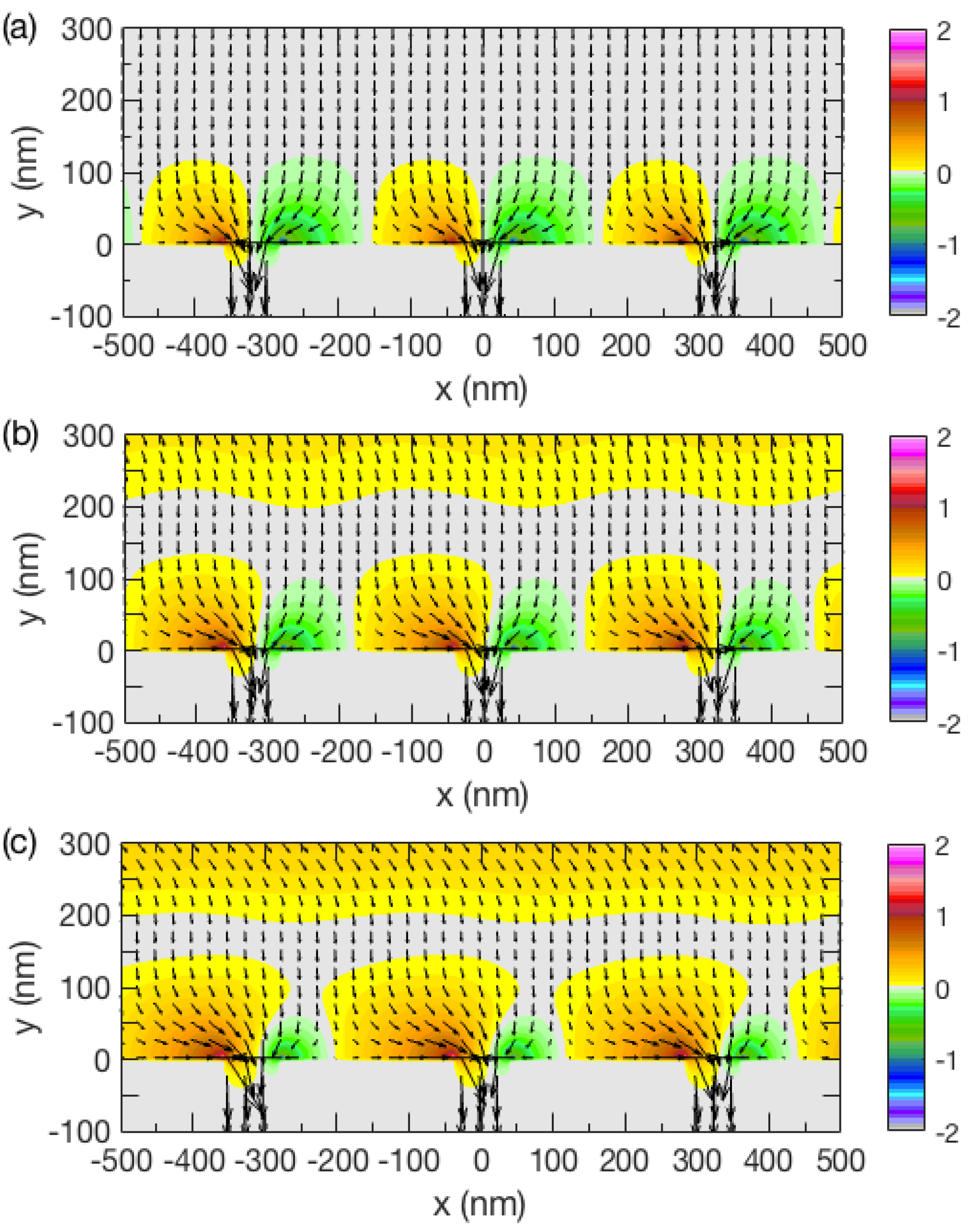
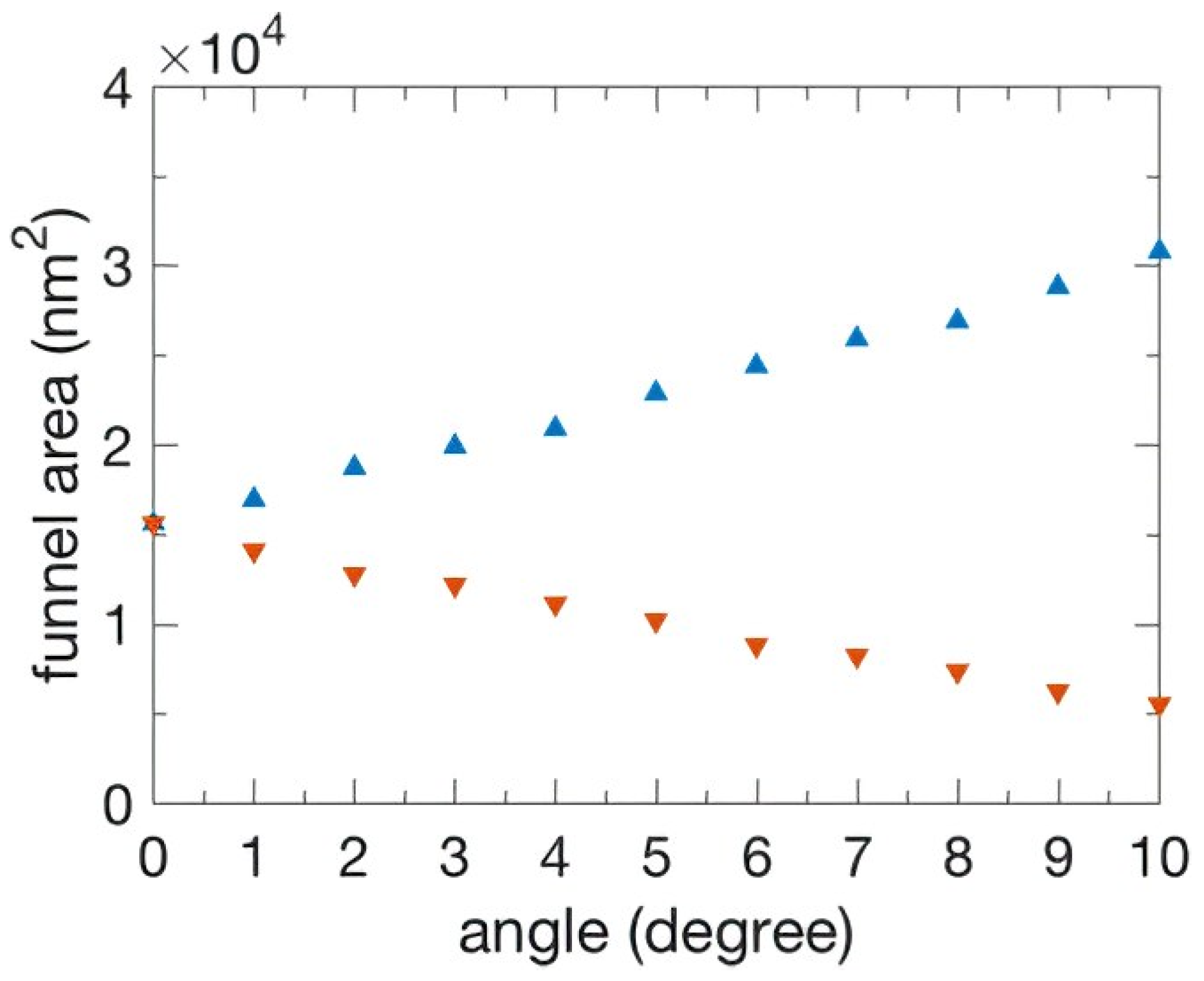
3.1. Asymmetric Funneling at Oblique Incidence

The simulation results of time-averaged Poynting vectors fields of a p-polarized plane wave illuminating a PEC film at different angles are shown in Figure 1. The colored contours represent where the Poynting vectors Sx ≠ 0. The funneling boundary is the region between the grey and colored contours where the wave flows into the slit. The boundary enclosing the colored contours is the funnel area.
At normal incidence, the time-averaged Poynting vectors for incident energy flow were equidistant as they flowed along the propagation direction as indicated in Figure 1a. As the energy flowed into the slits, the funneling sizes near the slits were symmetrical and equal in magnitude. When the fields penetrated into the metal, the field distribution was also symmetrical and equal in magnitude. In contrast, at small incident angles 5° and 10° to the normal, the penetrated field distributions inside the metal became highly asymmetrical as shown in Figure 1b,c. The funneling size and the magnitude to the left of each slit was increased while the size to the right was decreased. This was more evident as the angle of incidence was increased. For both cases, the energy flow entered at an angle until y ≈ 200 nm; it was turned to downward only in the case of normal incidence until y ≈ 125 nm; and it was then returned back to its original angle of incidence again before funneling into the slits. We found this to be an interesting continuation of normal incidence; as observed in the second region, (200 nm > y > 125 nm) would be expected. For example, when the angle of the incident wave was 10°, the field had a minima Savg = 0 at y ≈ 162 nm and 487 nm and a maxima Savg ≈ 0.35 at y ≈ 0 nm, 325 nm, and 650 nm. The energy flows were bent from y = 325 nm to 162 nm, straight at y = 162 nm, and bent again from y = 162 nm to 0 nm.
The symmetry of the funnel boundary was manipulated when the angle of the incident light was changed. At incident angles 0°, 5°, and 10°, the width of the left (right) boundary was 160 nm (160 nm), 198 nm (122 nm), and 230 nm (90 nm), respectively. The sum of the funnel widths was λ/2 = 320 nm due to the periodicity of the slits. When the left (right) width of the boundary became larger (smaller), the left (right) height of the boundary increased (decreased) as the incident angle simultaneously increased. As shown in Figure 2, the left (right) funnel area for incident angles 0°, 5°, and 10° was 1.56 × 10⁴ (1.56 × 10⁴) nm2, 2.29 × 10⁴ (1.02 × 10⁴) nm2, and 3.08 × 10⁴ (0.55 × 10⁴) nm2, respectively.
We found that more (less) EM wave energy flow redirected inside the left (right) funnel area under oblique incidence. An interesting feature was that, as the symmetry of the funnel widths was broken, the left (right) funnel width was increased (decreased) as the energy flow increased (decreased). Thus, the transmitted energy was positively correlated to the funnel area.

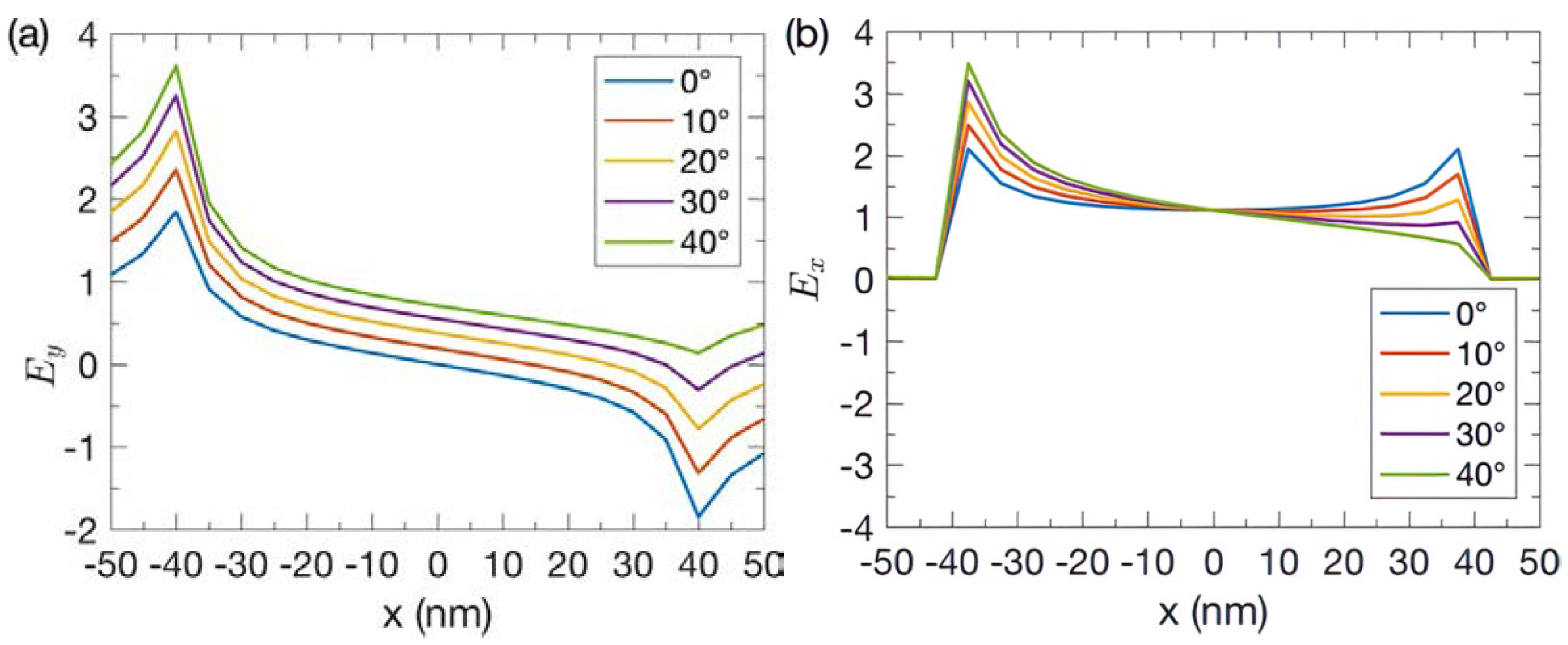
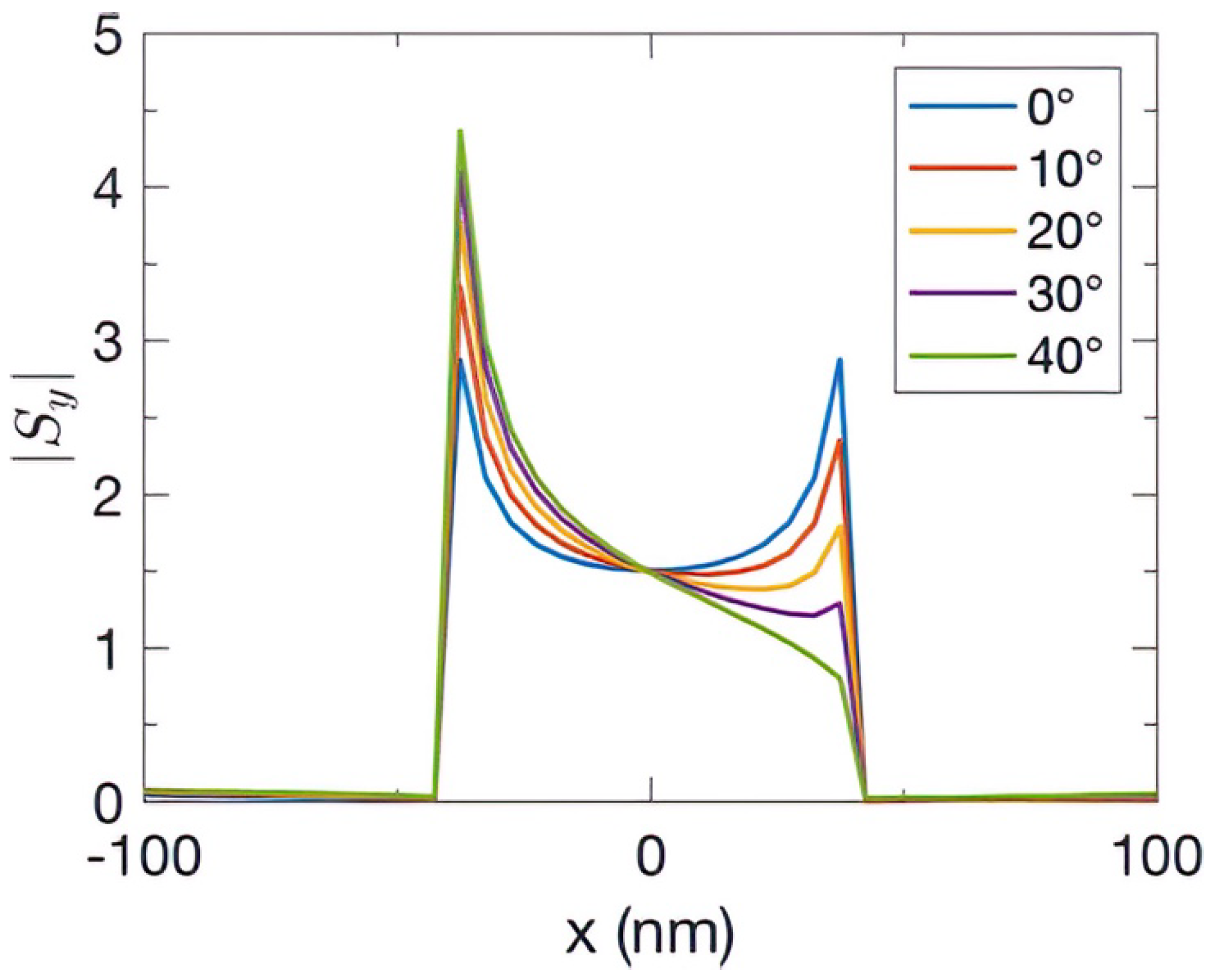
3.2. Mechanism of Asymmetrical Funneling

The light funneling effect is an interaction between the incident fields and charges induced around the corners [54]. As shown in Figure 1, the fields penetrated into the metal at the corners of the slits and we could clearly observe the penetrating field distributions. When the angle of incidence was normal to the PEC, the penetrating fields at both corners were symmetrical. As the angle was increased from 0° to 5° to 10°, the penetrating field distribution became nonsymmetrical; the penetrating fields in the left corner became greater than that of the right corner. The penetrating fields at the corners were linearly proportional to the accumulated induced charges as they had to be self-consistent to satisfy Maxwell’s equations. Thus, the field distribution corresponded to charge distributions at the corners.
When the incident wave reached the PEC at y = 0, its propagation path was changed. While the y component of the electric field changed, the magnetic field remained constant. As the angle of incidence was increased, the amplitude of their instant normalized electric field at the left (right) corner also increased (decreased), as shown in Figure 3, when the magnetic field at the left corner reached its positive maximum. The increase (decrease) of the vertical electric field Ey at the left (right) corner as indicated in Figure 3a changed the energy flow at the interface. This affected the funnel boundary as the horizontal boundary of the funneling profile was defined by the Poynting vector for the x component Sx, which is proportional to Ey × Hz. The phase of the vertical electric field Ey in the left (right) side decided the x component of the Poynting vector to be positive (negative). As the angle of incidence increased, the left (right) side boundary of the light funnel enlarged (decreased). The funnel width was determined by the electric field normal to the film.
The asymmetrical funneling effect was further examined quantitatively by studying the horizontal electric field Ex near the slit entrance, as shown in Figure 3b. The Poynting vector for the y component Sy was proportional to −Ex × Hz. As the angle of incidence was increased, the amplitude of the horizontal electric field Ex in the left (right) corner of the central subwavelength slit was increased (decreased) as well. The surface charges at the left corners accumulated. The edges further enhanced the local electric field, the Poynting vectors, and the funneling. Regarding the edge effect at the left corner, the horizontal electric field Ex moved the charges on the surface to form the current towards the +x direction. The vertical electric field induced the current on the slit surface in the +y direction so that more positive charges accumulated to enhance the local electric field. At oblique incidence, the electric field at the right corner had a different phase, which should be considered for understanding the detailed mechanism.
Figure 4 shows the magnitude of the normalized Poynting vector of the y component |Sy| at the interface y = 0 for different incident angles. At normal incidence, the magnitude of the directional energy flux at both the corners of the center slit were |Sy| = 2.87. When the angle of incidence was increased, e.g., 40°, |Sy| was 4.36 (0.80) in the left (right) hot spot. The magnitude of |Sy| was proportional to the magnetic field Hz of the incident wave, and the sharpness at the edges was directly proportional to the number of accumulated charges. If the intensity of the spike increased, the amount of local energy funneled into the slit increased. On the other hand, the total energy fluxes, calculated by the integration over x at t = 3.3 T, were 146.20, 145.48, 143.62, 142.11, and 139.56 for angles of incidence 0°, 10°, 20°, 30°, and 40°, respectively. The total energy flux only slightly decreased when the incident angle was increased. This insensitivity to the incident light angle is academically interesting because the flux of light passing through an oblique plane is well-known to decrease significantly with the angle. In addition, this funneling feature is important for photonic applications.

4. Conclusions

We studied the funneling mechanism of oblique light incidence at the entrances of metallic subwavelength slits using FDTD simulations. In contrast to previous studies, we found that the funneling can be highly asymmetric for obliquely incident light, although the energy flow turns to downward only at normal incidence at a region near the surface. The mechanism is explained by induced fields, which correspond to polarization charges, using Poynting vectors. Regarding the dynamics of wave-charge interaction, accumulated fields and charges at the sharp edges of the slits caused the nearby light energy to flow into the slit, further enhancing light transmission. When light is incident obliquely from the left (right) side of the nano slit, asymmetric and more (less) polarized fields and charges are accumulated at the upper apex corner of the left (right) side, respectively, thus increasing (decreasing) the funnel width, area, and energy flow on the left (right) side. The total transmitted energy flux is insensitive to the incident light angle, in contrast to the light flux passing through an oblique plane. In addition to the academic significance for further understanding of the angle of incidence effect on light funneling, this study is useful for the development of subwavelength-scale plasmonic applications.

Author Contributions

Conceptualization, K.-R.C., A.E.C., J.-S.H. and X.-Q.X.; software, J.-S.H., K.-R.C. and A.E.C.; investigation, K.-R.C., X.-Q.X., A.E.C. and J.-S.H.; data curation, X.-Q.X., A.E.C. and K.-R.C.; validation, A.E.C. and K.-R.C.; writing—original draft preparation, A.E.C. and X.-Q.X.; writing—review and editing, K.-R.C., A.E.C. and X.-Q.X.; supervision, A.E.C., J.-S.H. and K.-R.C.; project administration, K.-R.C.; funding acquisition, K.-R.C. All authors have read and agreed to the published version of the manuscript.

Funding

This research was funded by the Ministry of Science and Technology (MOST), grant numbers 107-2112-M-006-011, 108-2112-M-006-014, 110-2112-M-006-008, 111-2112-M-006-012.

Data Availability Statement

The authors confirm that the data supporting the findings of this study are available within this paper.

Acknowledgments

We gratefully acknowledge support from the Ministry of Science and Technology (MOST) (2112-M-006-011, 108-2112-M-006-014, 110-2112-M-006-008, 111-2112-M-006-012) and the computing resources provided on Taiwania, a high-performance computing cluster operated by the National Center for High-performance Computing (NCHC) at National Applied Research Laboratories (NARLabs).

Conflicts of Interest

The authors declare no conflict of interest.

References

  1. Bethe, H.A. Theory of Diffraction by Small Holes. Phys. Rev. 1944, 66, 163. [Google Scholar] [CrossRef]
  2. Ebbesen, T.W.; Lezec, H.J.; Ghaemi, H.F.; Thio, T.; Wolff, P.A. Extraordinary optical transmission through sub-wavelength hole arrays. Nature 1998, 391, 667–669. [Google Scholar] [CrossRef]
  3. Porto, J.A.; García-Vidal, F.J.; Pendry, J.B. Transmission Resonances on Metallic Gratings with Very Narrow Slits. Phys. Rev. Lett. 1999, 83, 2845–2848. [Google Scholar] [CrossRef] [Green Version]
  4. Takakura, Y. Optical Resonance in a Narrow Slit in a Thick Metallic Screen. Phys. Rev. Lett. 2001, 86, 5601–5603. [Google Scholar] [CrossRef] [PubMed]
  5. Pardo, F.; Bouchon, P.; Haïdar, R.; Pelouard, J.L. Light Funneling Mechanism Explained by Magnetoelectric Interference. Phys. Rev. Lett. 2011, 107, 093902. [Google Scholar] [CrossRef] [Green Version]
  6. Li, J.W.; Hong, J.S.; Chou, W.T.; Huang, D.J.; Chen, K.R. Light funneling profile during enhanced transmission through a subwavelength metallic slit. Plasmonics 2018, 13, 2249–2254. [Google Scholar] [CrossRef]
  7. Hong, J.S.; Chen, A.E.; Chen, K.R. Modulated light transmission through a subwavelength slit at early stage. Opt. Express 2015, 23, 9901–9910. [Google Scholar] [CrossRef] [Green Version]
  8. Chen, A.E.; Hong, J.S.; Chen, K.R. Physics of anomalous transient light transmission through subwavelength metallic slit. Plasmonics 2021, 16, 915–922. [Google Scholar] [CrossRef]
  9. Nikitin, A.Y.; Zueco, D.; García-Vidal, F.J.; Martín-Moreno, L. Electromagnetic wave transmission through a small hole in a perfect electric conductor of finite thickness. Phys. Rev. B 2008, 78, 165429. [Google Scholar] [CrossRef] [Green Version]
  10. Chang, S.H.; Su, Y.L. Mapping of transmission spectrum between plasmonic and nonplasmonic single slits. I: Resonant transmission. J. Opt. Soc. Am. B 2015, 32, 38–44. [Google Scholar] [CrossRef]
  11. Chang, S.H.; Su, Y.L. Mapping of transmission spectrum between plasmonic and nonplasmonic single slits. II: Nonresonant transmission. J. Opt. Soc. Am. B 2015, 32, 45–51. [Google Scholar] [CrossRef]
  12. Astilean, S.; Lalanne, P.; Palamaru, M. Light transmission through metallic channels much smaller than the wavelength. Opt. Commun. 2000, 175, 265–273. [Google Scholar] [CrossRef]
  13. Liu, H.T.; Lalanne, P. Microscopic theory of the extraordinary optical transmission. Nature 2008, 452, 728–731. [Google Scholar] [CrossRef] [PubMed]
  14. Pendry, J.B.; Martín-Moreno, L.; Garcia-Vidal, F.J. Mimicking Surface Plasmons with Structured Surfaces. Science 2004, 305, 847–848. [Google Scholar] [CrossRef] [PubMed]
  15. van Beijnum, F.; Retif, C.; Smiet, C.B.; Liu, H.T.; Lalanne, P.; van Exter, M.P. Quasi-cylindrical wave contribution in experiments on extraordinary optical transmission. Nature 2012, 492, 411–414. [Google Scholar] [CrossRef]
  16. Chen, K.R. Focusing of light beyond the diffraction limit of half the wavelength. Opt. Lett. 2010, 35, 3763–3765. [Google Scholar] [CrossRef] [PubMed] [Green Version]
  17. Chen, K.R.; Chu, W.H.; Fang, H.C.; Liu, C.P.; Huang, C.H.; Chui, H.C.; Chuang, C.H.; Lo, Y.L.; Lin, C.Y.; Hwung, H.H.; et al. Beyond-limit light focusing in the intermediate zone. Opt. Lett. 2011, 36, 4497–4499. [Google Scholar] [CrossRef] [PubMed] [Green Version]
  18. Novotny, L.; van Hulst, N. Antennas for light. Nat. Photonics. 2011, 5, 83–90. [Google Scholar] [CrossRef]
  19. Kim, K.Y.; Goncharenko, A.V.; Hong, J.S.; Chen, K.R. Near-field Characterization on Light Emanated from Subwavelength Plasmonic Double Slit of Finite Length. J. Opt. Soc. Korea 2011, 15, 196–201. [Google Scholar] [CrossRef] [Green Version]
  20. Fang, N.; Lee, H.; Sun, C.; Zhang, X. Diffraction-Limited Optical Imaging with a Silver Superlens. Science 2005, 308, 534. [Google Scholar] [CrossRef]
  21. Catrysse, P.B.; Wandell, B.A. Integrated color pixels in 0.18-µm complementary metal oxide semiconductor technology. J. Opt. Soc. Am. A 2003, 20, 2293–2306. [Google Scholar] [CrossRef] [PubMed]
  22. Goncharenko, A.V.; Kim, K.Y.; Hong, J.S.; Chen, K.R. Complex mechanism of enhanced optical transmission through a composite coaxilal/circular aperture. Plasmonics 2012, 7, 417–426. [Google Scholar] [CrossRef]
  23. Xu, T.; Wu, Y.K.; Luo, X.; Guo, L.J. Plasmonic nanoresonators for high-resolution colour filtering and spectral imaging. Nat. Commun. 2010, 1, 59. [Google Scholar] [CrossRef] [PubMed] [Green Version]
  24. Rodrigo, S.G.; de León-Pérez, F.; Martín-Moreno, L. Extraordinary Optical Transmission: Fundamentals and Applications. Proc. IEEE 2016, 104, 2288–2306. [Google Scholar] [CrossRef] [Green Version]
  25. Hong, J.S.; Chen, K.R. Light diffraction by a slit and grooves with a point source model based on wave dynamics. Phys. Rev. A 2017, 96, 043813. [Google Scholar] [CrossRef]
  26. Karelits, M.; Lozitsky, E.; Chelly, A.; Zalevsky, Z.; Karsenty, A. Advanced Surface Probing Using a Dual-Mode NSOM–AFM Silicon-Based Photosensor. Nanomaterials 2019, 9, 1792. [Google Scholar] [CrossRef] [Green Version]
  27. Nalimov, A.; Kotlyar, V. Ultra-Thin, Short-Focus, and High-Aperture Metalens for Generating and Detecting Laser Optical Vortices. Nanomaterials 2022, 12, 2602. [Google Scholar] [CrossRef]
  28. Luo, M.Y.; Li, X.; Zhang, Z.J.; Ma, H.S.; Du, T.; Jiang, X.P.; Zhang, Z.R.; Yang, J.B. Tunable Infrared Detection, Radiative Cooling and Infrared-Laser Compatible Camouflage Based on a Multifunctional Nanostructure with Phase-Change Material. Nanomaterials 2022, 12, 2261. [Google Scholar] [CrossRef]
  29. Shah, Y.D.; Connolly, P.W.R.; Grant, J.P.; Hao, D.; Accarino, C.; Ren, X.; Kenney, M.; Annese, V.; Rew, K.G.; Greener, Z.M.; et al. Ultralow-light-level color image reconstruction using high-efficiency plasmonic metasurface mosaic filters. Optica 2020, 7, 632–639. [Google Scholar] [CrossRef]
  30. Sarkar, S.; Gupta, V.; Tsuda, T.; Gour, J.; Singh, A.; Aftenieva, O.; Steiner, A.M.; Hoffmann, M.; Kumar, S.; Fery, A.; et al. Plasmonic Charge Transfers in Large-Scale Metallic and Colloidal Photonic Crystal Slabs. Adv. Funct. Mater. 2021, 31, 202011099. [Google Scholar] [CrossRef]
  31. Bludov, Y.V.; Peres, N.M.R.; Vasilevskiy, M.I. Symmetric Graphene Dielectric Nanowaveguides as Ultra-Compact Photonic Structures. Phys. Rev. B 2020, 101, 075415. [Google Scholar] [CrossRef] [Green Version]
  32. Hong, J.S.; Chen, K.R. Inward electromagnetic wave coupling in hybrid subwavelength structures illuminated with secondary imaging. Chin. J. Phys. 2021, 72, 688–699. [Google Scholar] [CrossRef]
  33. Elshorbagy, M.H.; Cuadrado, A.; Alda, J. Plasmonic Sensors Based on Funneling Light Through Nanophotonic Structures. Plasmonics 2020, 15, 915–921. [Google Scholar] [CrossRef] [Green Version]
  34. Chen, C.M.; Young, C.K.; Chen, K.R.; Lan, Y.C. Spiral surface plasmon modes on uniform and tapered metallic nanorods. J. Opt. Soc. Am. B 2013, 30, 2529–2534. [Google Scholar] [CrossRef]
  35. Salman, D.; Prince, B. Pyramid-shaped plasmonic slit for optical transmission. Opt. Mater. 2019, 88, 266–270. [Google Scholar]
  36. Hong, J.S.; Wang, T.K.; Chen, A.E.; Li, H.N.; Chen, K.R. Source Image Squeezing and Field Tunneling for Propagating Light Beyond-Limit Focusing to Reach the Intermediate Zone. Plasmonics 2020, 16, 619–628. [Google Scholar] [CrossRef]
  37. Novotny, L.; Hecht, B. Principles of Nano-Optics, 3rd ed.; Cambridge University Press: Cambridge, UK, 2006; pp. 154–196. [Google Scholar]
  38. Vincenti, M.A.; de Ceglia, D.; Buncick, M.; Akozbek, N.; Bloemer, M.J.; Scalora, M. Extraordinary transmission in the ultraviolet range from subwavelength slits on semiconductors. J. Appl. Phys. 2010, 107, 053101. [Google Scholar] [CrossRef] [Green Version]
  39. García-Vidal, F.J.; Martín-Moreno, L. Transmission and focusing of light in one-dimensional periodically nanostructured metals. Phy. Rev. B 2002, 66, 155412. [Google Scholar] [CrossRef]
  40. Zeng, Y.; Fu, Y.; Chen, X.S.; Lu, W.; Agren, H. Dynamics of the damping oscillator formed by the collective generation of surface polaritons for extraordinary light transmission through subwavelength hole arrays in thin metal films. Phy. Rev. B 2007, 76, 8. [Google Scholar] [CrossRef]
  41. Zhu, P.; Jin, P.; Shi, H.; Guo, L.J. Funneling light into subwavelength grooves in metal/dielectric multilayer films. Opt. Express 2013, 21, 3595–3602. [Google Scholar] [CrossRef]
  42. Jazayeri, A.M.; Mehrany, K. All-dielectric structure for trapping nanoparticles via light funneling and nanofocusing. J. Opt. Soc. Am. B 2017, 34, 2179–2184. [Google Scholar] [CrossRef]
  43. Kamalieva, A.N.; Toropov, N.A.; Vartanyan, T.A.; Baranov, M.A.; Parfenov, P.S.; Bogdanov, K.V.; Zharova, Y.A.; Tolmachev, V.A. Fabrication of Silicon Nanostructures for Application in Photonics. Semiconductors 2018, 52, 632–635. [Google Scholar] [CrossRef]
  44. Xi, Y.G.; Jung, Y.S.; Kim, H.K. Interaction of light with a metal wedge: The role of diffraction in shaping energy flow. Opt Express 2010, 18, 2588–2600. [Google Scholar] [CrossRef] [PubMed]
  45. Lee, J.W.; Seo, M.A.; Sohn, J.Y.; Ahn, Y.H.; Kim, D.S.; Jeoung, S.C.; Lienau, C.; Park, Q.H. Invisible plasmonic meta-materials through impedance matching to vacuum. Opt. Express 2005, 13, 10681–10687. [Google Scholar] [CrossRef]
  46. Han, Y.; Lin, Y.; Ma, W.; Korvink, J.G.; Duan, H.; Deng, Y. Nanoantennas Inversely Designed to Couple Free Space and a Metal–Insulator–Metal Waveguide. Nanomaterials 2021, 11, 3219. [Google Scholar] [CrossRef]
  47. Aminian, A.; Rahmat-Samii, Y. Spectral FDTD: A novel technique for the analysis of oblique incident plane wave on periodic structures. IEEE Trans. Antennas Propag. 2006, 54, 1818–1825. [Google Scholar] [CrossRef]
  48. Bortchagovsky, E.; des Francs, G.C.; Molenda, D.; Naber, A.; Fischer, U.C. Transmission of an obliquely incident beam of light through small apertures in a metal film. Appl. Phys. B 2006, 84, 49–53. [Google Scholar] [CrossRef]
  49. Kim, W.; Guo, J.; Hendrickson, J. Subwavelength metal grating metamaterial for polarization-selective optical antireflection coating. J. Opt. Soc. Am. B 2015, 32, 1392–1398. [Google Scholar] [CrossRef] [Green Version]
  50. Tsai, C.H.; Chang, S.H.; Tseng, S.H. Applying the Optical Theorem in a Finite-Difference Time-Domain Simulation of Light Scattering. IEEE Trans. Antennas Propag. 2010, 58, 3091–3094. [Google Scholar] [CrossRef]
  51. Derby, J.J.; Atherton, L.J.; Gresho, P.M. An integrated process model for the growth of oxide crystals by the Czochralski method. J. Cryst. Growth 1989, 97, 792–826. [Google Scholar] [CrossRef]
  52. Villora, E.G.; Morioka, Y.; Atou, T.; Sugawara, T.; Kikuchi, M.; Fukuda, T. Infrared Reflectance and Electrical Conductivity of β-Ga2O3. Phys. Stat. Sol. 2002, 193, 187–195. [Google Scholar] [CrossRef]
  53. Ida, N. Engineering Electromagnetics, 3rd ed.; Springer International Publishing: Cham, Switzerland, 2015; p. 691. [Google Scholar]
  54. Xie, Y.; Zakharian, A.R.; Moloney, J.V.; Mansuripur, M. Transmission of light through slit apertures in metallic films. Opt. Express 2004, 12, 6106–6121. [Google Scholar] [CrossRef] [PubMed]
Figure 1. The time-averaged Poynting vector fields of light energy funneling at incident angle (a) 0°, (b) 5°, and (c) 10° into subwavelength grooves etched in a perfect electric conductor.
Nanomaterials 13 00061 g001
Figure 2. The relationship between funnel area and the angle of incidence. The left (right) funnel area is indicated by the blue upward-triangle (orange downward-triangle).
Nanomaterials 13 00061 g002
Figure 3. The amplitude of instant normalized electric fields (a) Ey and (b) Ex at the PEC vacuum-interface (y = 0) at various incident angles.
Nanomaterials 13 00061 g003
Figure 4. The magnitude of normalized Poynting vector of the y component |Sy| at the PEC interface, y = 0, at various incident angles, when the magnetic field at the left corner reaches its positive maximum.
Nanomaterials 13 00061 g004
Disclaimer/Publisher’s Note: The statements, opinions and data contained in all publications are solely those of the individual author(s) and contributor(s) and not of MDPI and/or the editor(s). MDPI and/or the editor(s) disclaim responsibility for any injury to people or property resulting from any ideas, methods, instructions or products referred to in the content.

