
Recent Development in Metasurfaces: A Focus on Sensing Applications


Abstract
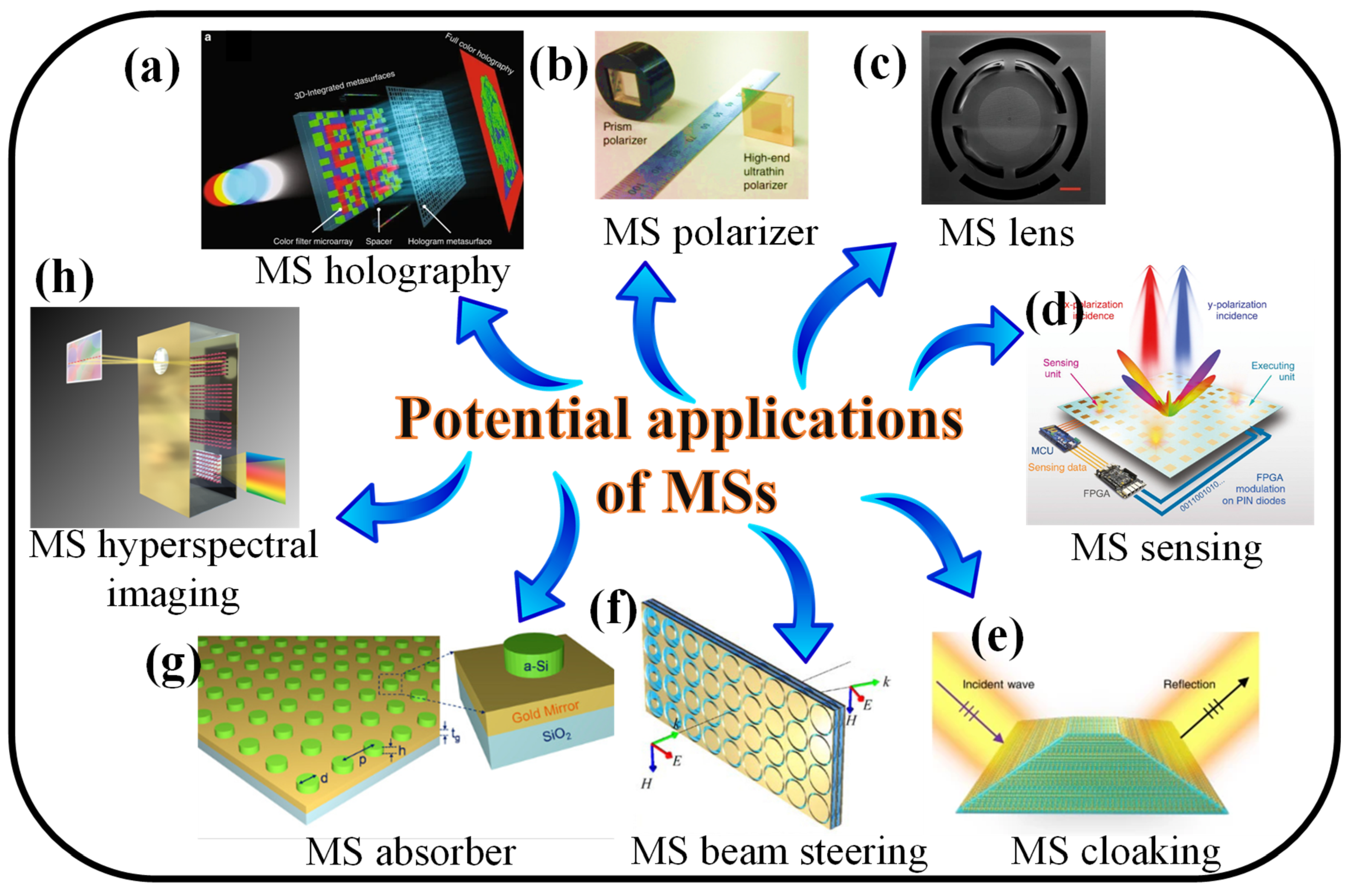
:1. Introduction

2. Requirements for Sensor Designing
3. Working Mechanism of the MS-Based Sensors
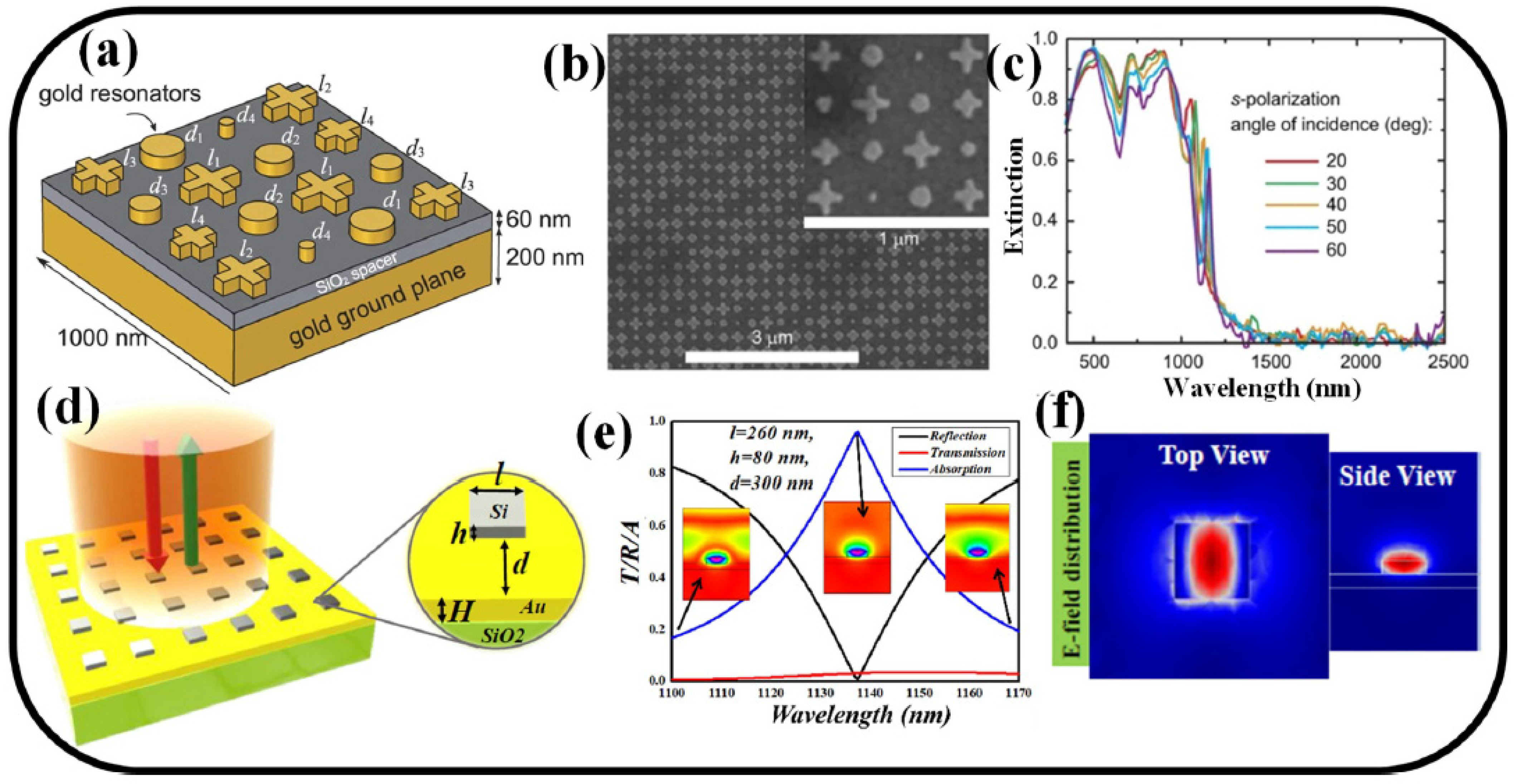
4. MS-Based Perfect Absorbers for Sensing Applications
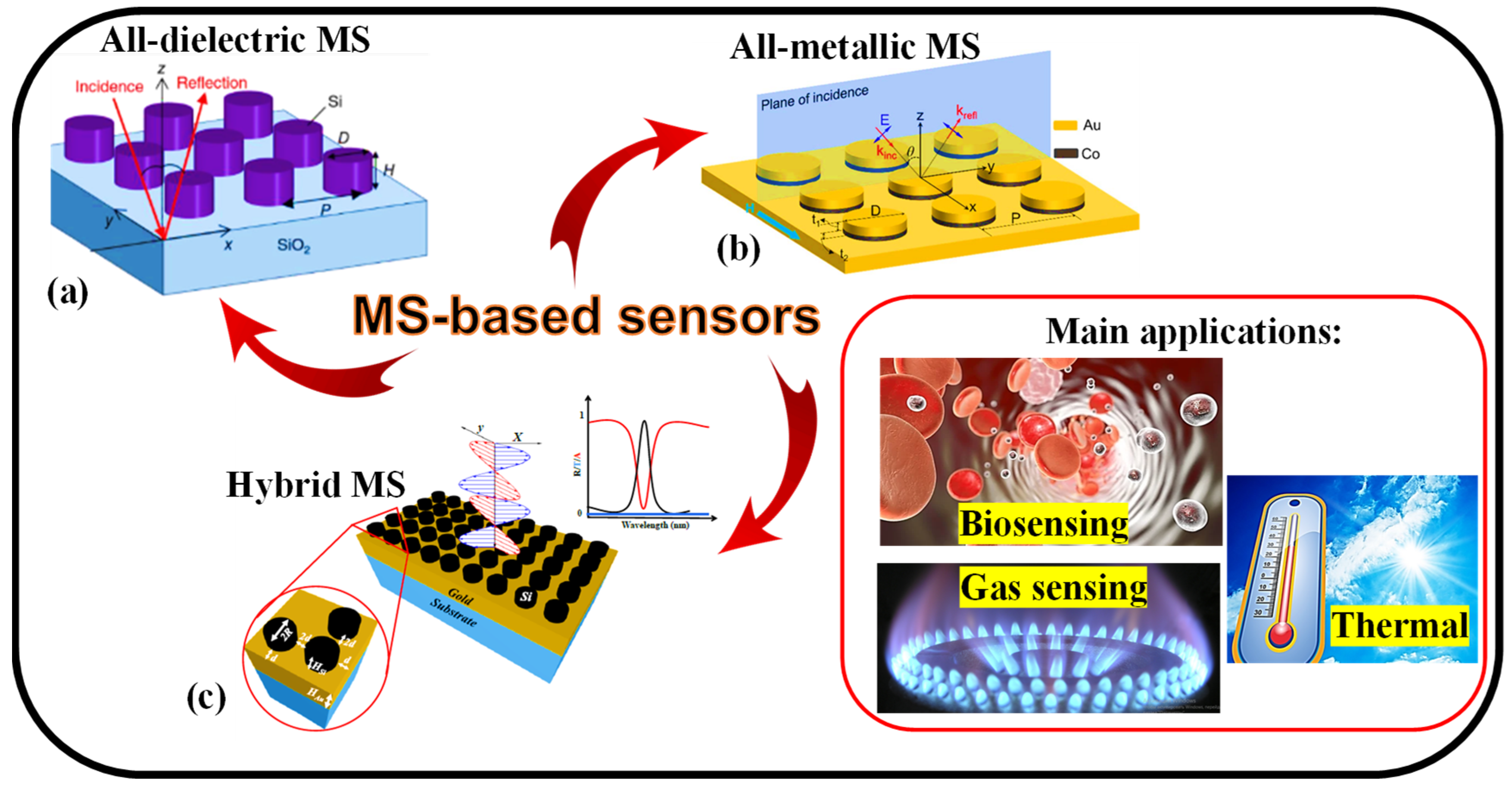
5. Types of MS-Based Sensors
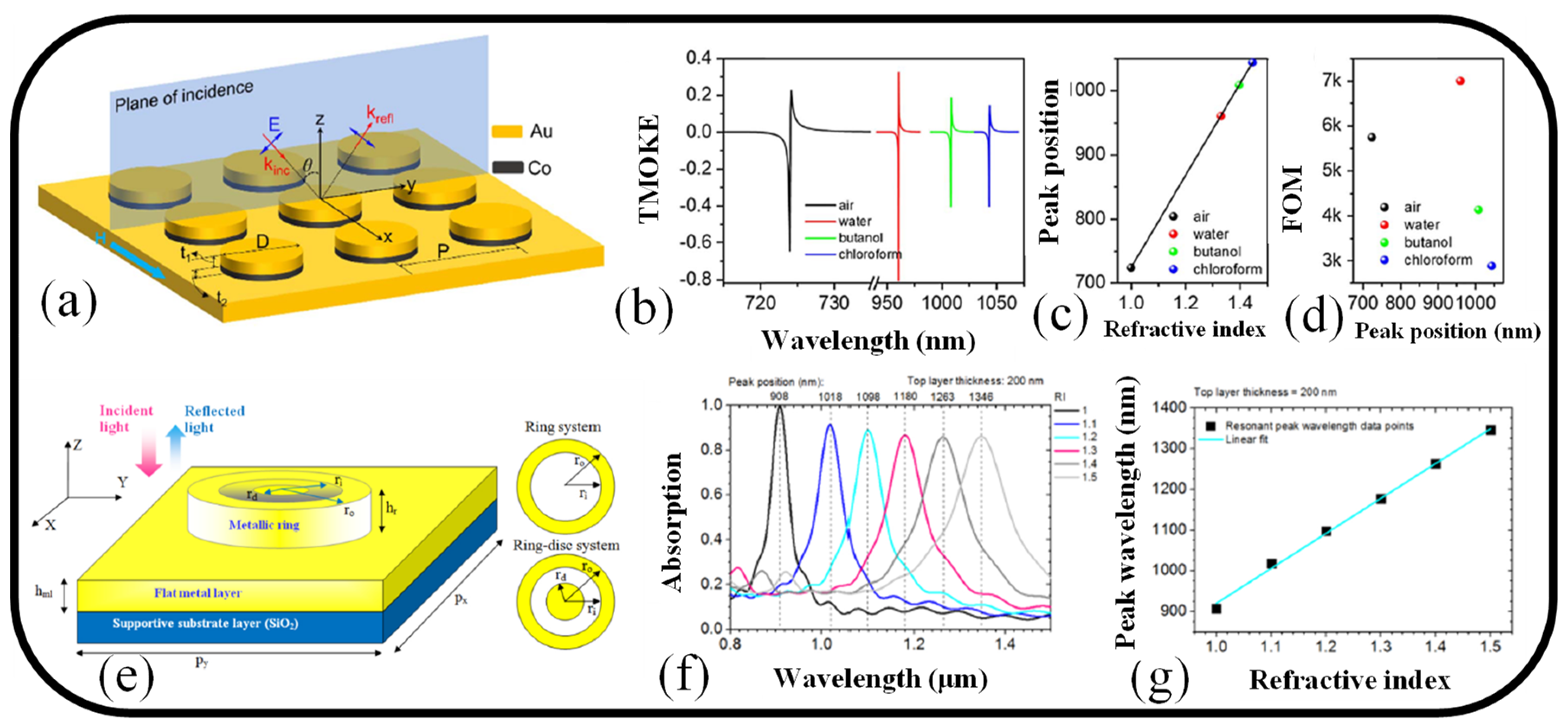
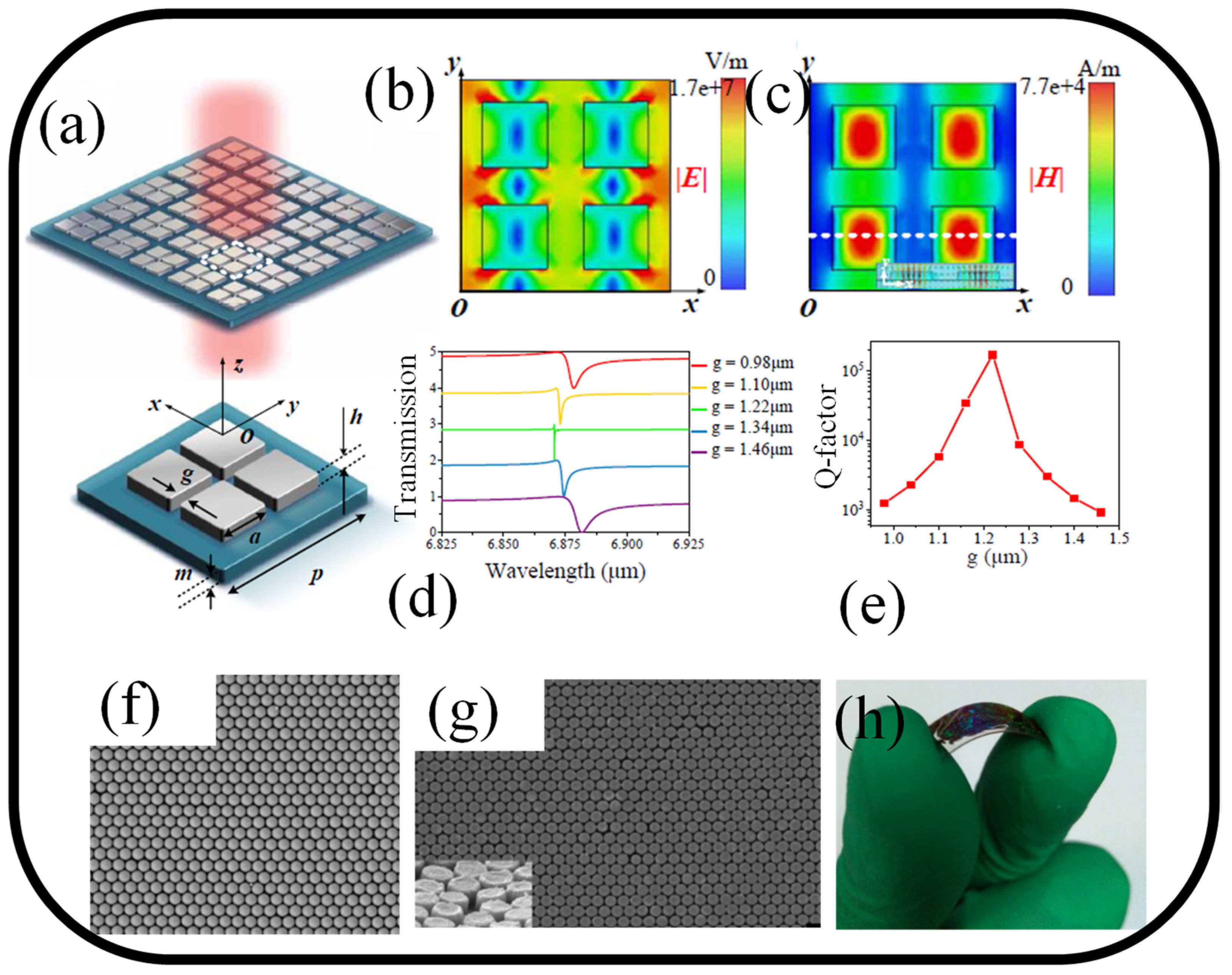
5.1. All-Metallic MS-Based Sensors
5.2. All-Dielectric MS-Based Sensors
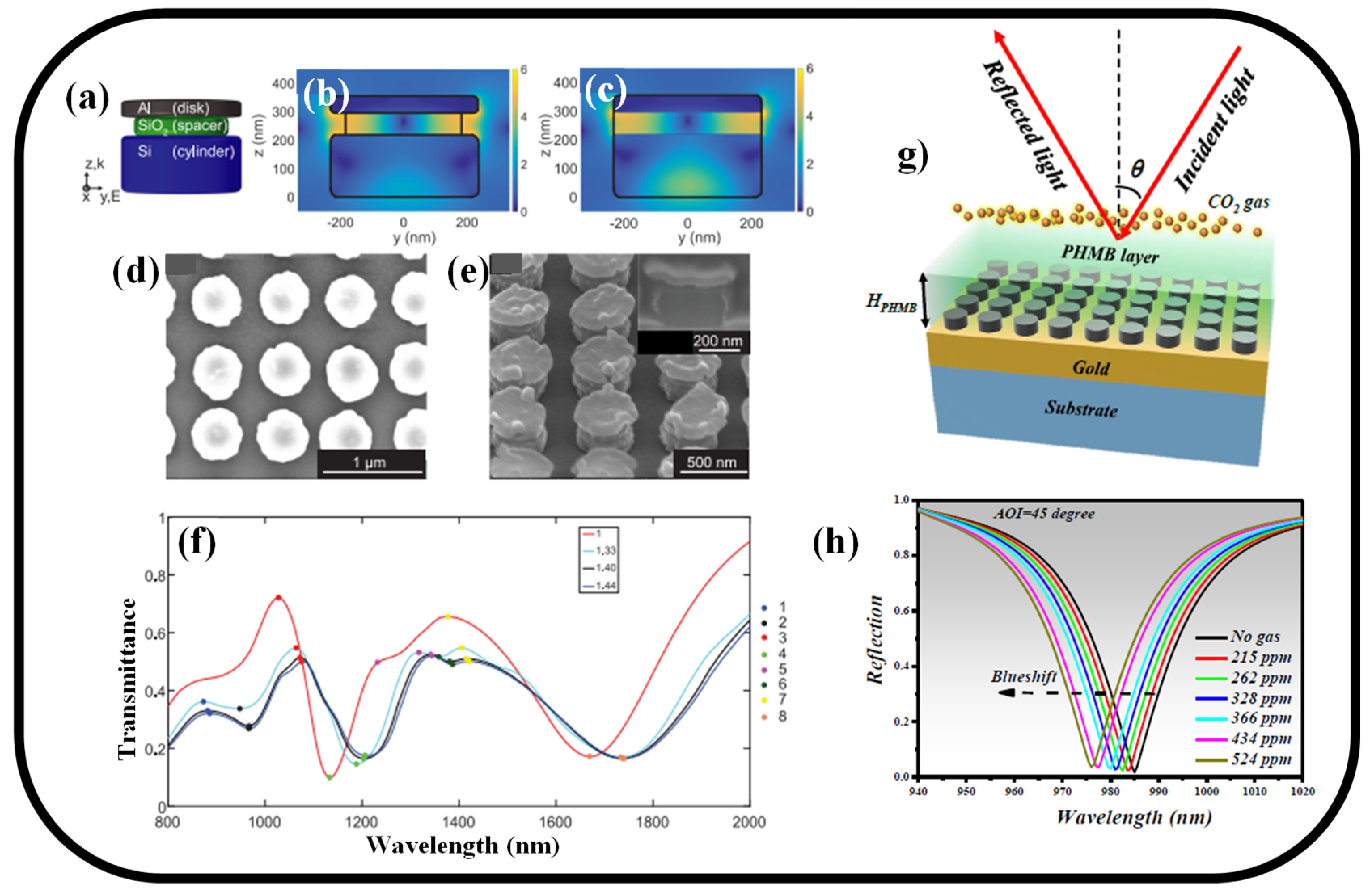
5.3. Hybrid MS-Based Sensors
6. Prospects and Challenges
7. Conclusions
Author Contributions
Funding
Institutional Review Board Statement
Informed Consent Statement
Data Availability Statement
Acknowledgments
Conflicts of Interest
Abbreviations
References
- Vargas, M.P. Fundamentals of metamaterial structures. In Planar Metamaterials Based Microwave Sensor Arrays for Biomedical Analysis and Treatment; Springer: Cham, Switzerland, 2014; pp. 7–31. [Google Scholar]
- Motcheyo, A.; Kanaa, T.; Essiane, S. Backward-energy propagation in nonlinear magnetic metamaterials. J. Supercond. Nov. Magn. 2021, 34, 2619–2626. [Google Scholar] [CrossRef]
- Zhai, S.; Zhao, X.; Liu, S.; Shen, F.; Li, L.; Luo, C. Inverse doppler effects in broadband acoustic metamaterials. Sci. Rep. 2016, 6, 32388. [Google Scholar] [CrossRef] [Green Version]
- Tyukhtin, A.; Vorobev, V. Cherenkov radiation in a metamaterial comprised of coated wires. J. Opt. Soc. Am. B 2013, 30, 1524–1531. [Google Scholar] [CrossRef]
- Valentine, J.; Zhang, S.; Zentgraf, T.; Ulin-Avila, E.; Genov, D.A.; Bartal, G.; Zhang, X. Three-dimensional optical metamaterial with a negative refractive index. Nature 2008, 455, 376–379. [Google Scholar] [CrossRef]
- Cheng, B.; Lan, Y.-C.; Tsai, D. Breaking optical diffraction limitation using optical hybrid-super-hyperlens with radially polarized light. Opt. Express 2013, 21, 14898–14906. [Google Scholar] [CrossRef]
- Cai, W.; Chettiar, U.; Kildishev, A.; Shalaev, V. Optical cloaking with metamaterials. Nat. Photonics 2007, 1, 224–227. [Google Scholar] [CrossRef] [Green Version]
- Orazbayev, B.; Beruete, M.; Khromova, I. Tunable beam steering enabled by graphene metamaterials. Opt. Express 2016, 24, 8848–8861. [Google Scholar] [CrossRef] [Green Version]
- Jaksic, Z.; Vukovic, S.; Matovic, J.; Tanaskovic, D. Negative refractive index metasurfaces for enhanced biosensing. Materials 2011, 4, 1–36. [Google Scholar] [CrossRef] [Green Version]
- Ishimaru, A.; Jaruwatanadilok, S.; Kuga, Y. Generalized surface plasmon resonance sensors using metamaterials and negative index materials. Progress Electromagn. Res. 2005, 51, 139–152. [Google Scholar] [CrossRef] [Green Version]
- Shamonin, M.; Radkovskaya, O.; Stevents, C.; Faulkner, G.; Edwards, D.; Sydoruk, O.; Zhuromskyy, O.; Shamonina, E.; Solymar, L. Waveguide and sensor systems comprising metamaterial element. In Proceedings of the DPG-Spring Meeting of the Division Condensed Matter, Dresden, Germany, 26–31 March 2006; pp. 114–118. [Google Scholar]
- Huang, M.; Yang, J. Microwave Sensor Using Metamaterials; Intech Press: Vienna, Austria, 2011; pp. 13–36. [Google Scholar]
- Evlyukhin, A.; Reinhardt, C.; Zywietz, U.; Chichkov, B. Collective resonances in metal nanoparticle arrays with dipole-quadrupole interactions. Phys. Rev. B 2012, 85, 245411. [Google Scholar] [CrossRef]
- Aristov, A.; Zywietz, U.; Evlyukhin, A.; Reinhardt, C.; Chichkov, B.; Kabashin, A. Laser-ablative engineering of phase singularities in plasmonic metamaterial arrays for biosensing applications. Appl. Phys. Lett. 2014, 104, 071101. [Google Scholar] [CrossRef]
- Hicks, E.; Zou, S.; Schatz, G.; Spears, K.; Duyne, R.; Gunnarsson, L.; Rindzevicius, T.; Kasemo, B.; Kall, M. Controlling plasmon line shapes through diffractive coupling in linear arrays of cylindrical nanoparticles fabricated by electron beam lithography. Nano Lett. 2005, 5, 1065–1070. [Google Scholar] [CrossRef]
- Li, F.; Hu, R. Metamaterials-enabled sensing for human-machine interfacing. Sensors 2021, 21, 161. [Google Scholar] [CrossRef]
- Li, L.; Ruan, H.; Liu, C.; Li, Y.; Shuang, Y.; Alu, A.; Qiu, C.-W.; Cui, T. Machine-learning reprogrammable metasurface imager. Nat. Commun. 2019, 10, 1082. [Google Scholar] [CrossRef] [Green Version]
- Khurgin, J. How to deal with the loss in plasmonics and metamaterials. Nat. Nano 2015, 10, 2–6. [Google Scholar] [CrossRef] [PubMed]
- Hu, J.; Bandyopadhyay, S.; Liu, Y.-H.; Shao, L.-Y. A Review on Metasurface: From Principle to Smart Metadevices. Front. Phys. 2021, 8, 1–20. [Google Scholar] [CrossRef]
- Sugimoto, H.; Fujii, M. Colloidal Mie resonators for all-dielectric metaoptics. Adv. Photonics Res. 2021, 2, 2000111. [Google Scholar] [CrossRef]
- Evlyukhin, A.; Reinhardt, C.; Seidel, A.; Luk’yanchuk, B.; Chichkov, B. Optical response features of Si-nanoparticle arrays. Phys. Rev. B 2010, 82, 045404. [Google Scholar] [CrossRef] [Green Version]
- Garcia-Etxarri, A.; Gomez-Medina, R.; Froufe-Perez, L.; Lopez, C.; Chantada, L.; Scheffold, F.; Aizpurua, J.; Nieto-Vesperinas, M.; Saenz, J. Strong magnetic response of submicron silicon particles in the infrared. Opt. Express 2011, 19, 4815–4826. [Google Scholar] [CrossRef] [Green Version]
- Kuznetsov, A.; Miroshnichenko, A.; Fu, Y.; Zhang, J.; Luk’yanchuk, B. Magnetic light. Sci. Rep. 2012, 2, 492. [Google Scholar] [CrossRef]
- Evlyukhin, A.; Novikov, S.; Zywietz, U.; Eriksen, R.; Reinhardt, C.; Bozhevolnyi, S.; Chichkov, B. Demonstration of magnetic dipole resonances of dielectric nanospheres in the visible region. Nano Lett. 2012, 12, 3749–3755. [Google Scholar] [CrossRef] [PubMed]
- Cardin, A.; Fan, K.; Padilla, W. Role of loss in all-dielectric metasurfaces. Opt. Express 2018, 26, 17669–17679. [Google Scholar] [CrossRef] [PubMed]
- Genevet, P.; Capasso, F.; Aieta, F.; Khorasaninejad, M.; Devlin, R. Recent advances in planar optics: From plasmonic to dielectric metasurfaces. Optica 2017, 4, 139–152. [Google Scholar] [CrossRef] [Green Version]
- Yang, Y.; Kravchenko, I.; Briggs, D.; Valentine, J. All-dielectric metasurface analogue of electromagnetically induced transparency. Nat. Commun. 2014, 5, 5753. [Google Scholar] [CrossRef] [Green Version]
- Liu, Y.-C.; Li, B.-B.; Xiao, Y.-F. Electromagnetically induced transparency in optical microcavities. Nanophotonics 2017, 6, 789–811. [Google Scholar] [CrossRef]
- Huang, Y.; Luo, J.; Pu, M.; Guo, Y.; Zhao, Z.; Ma, X.; Li, X.; Luo, X. Catenary electromagnetics for ultra-broadband lightweight absorbers and large-scale flat antennas. Adv. Sci. 2019, 6, 1801691. [Google Scholar] [CrossRef] [Green Version]
- Javaid, M.; Haleem, A.; Singh, R.; Rab, S.; Suman, R. Significance of sensors for industry 4.0: Roles, capabilities, and applications. Sens. Int. 2021, 2, 100110. [Google Scholar] [CrossRef]
- Hu, Y.; Luo, X.; Chen, Y.; Liu, Q.; Li, X.; Wang, Y.; Liu, N.; Duan, H. 3D-integrated metasurfaces for full-colour holography. Light Sci. Appl. 2019, 8, 86. [Google Scholar] [CrossRef] [Green Version]
- Kurosawa, H.; Choi, B.; Sugimoto, Y.; Iwanaga, M. High-performance metasurface polarizers with extinction ratios exceeding 12000. Opt. Express 2017, 25, 4446–4455. [Google Scholar] [CrossRef]
- Arbabi, E.; Arbabi, A.; Kamali, S.; Horie, Y.; Faraji-Dana, M.; Faraon, A. MEMS-tunable dielectric metasurface lens. Nat. Commun. 2018, 9, 812. [Google Scholar] [CrossRef]
- Ma, Q.; Hong, Q.; Gao, X.; Jing, H.; Liu, C.; Bai, G.; Cheng, Q.; Cui, T. Smart sensing metasurface with self-defined functions in dual polarizations. Nanophotonics 2020, 9, 3271–3278. [Google Scholar] [CrossRef]
- Xu, H.-X.; Hu, G.; Wang, Y.; Wang, C.; Wang, M.; Wang, S.; Huang, Y.; Genevet, P.; Huang, W.; Qiu, C.-W. Polarization-insensitive 3D conformal-skin metasurface cloak. Light Sci. Appl. 2021, 10, 75. [Google Scholar] [CrossRef]
- Wei, Z.; Cao, Y.; Su, X.; Gong, Z.; Long, Y.; Li, H. Highly efficient beam steering with a transparent metasurface. Opt. Express 2013, 21, 10739–10745. [Google Scholar] [CrossRef]
- Rifat, A.; Rahmani, M.; Xu, L.; Miroshnichenko, A. Hybrid Metasurface Based Tunable Near-Perfect Absorber and Plasmonic Sensor. Materials 2018, 11, 1091. [Google Scholar] [CrossRef] [Green Version]
- Faraji-Dana, M.; Arbabi, E.; Kwon, H.; Kamali, S.; Arbabi, A.; Bartholomew, J.; Faraon, A. Hyperspectral imager with folded metasurface optics. ACS Photonics 2019, 6, 2161–2167. [Google Scholar] [CrossRef] [Green Version]
- Lee, B.; Kim, Y.; Park, K.; Eom, J.; Kim, M.; Rho, B.; Choi, H. Interferometric fiber optic sensors. Sensors 2012, 12, 2467–2486. [Google Scholar] [CrossRef] [Green Version]
- Butt, M.A.; Degtyarev, S.A.; Khonina, S.N.; Kazanskiy, N.L. An evanescent field absorption gas sensor at mid-IR 3.39 um wavelength. J. Mod. Opt. 2017, 64, 1892–1897. [Google Scholar] [CrossRef] [Green Version]
- Leal-Junior, A.; Avellar, L.; Biazi, V.; Soares, M.; Frizera, A. Multifunctional flexible optical waveguide sensor: On the bioinspiration for ultrasensitive sensors development. Opto-Electron. Adv. 2022, 5, 210098. [Google Scholar] [CrossRef]
- Butt, M.A.; Khonina, S.N.; Kazanskiy, N.L. A highly sensitive design of subwavelength grating double-slot waveguide microring resonator. Laser Phys. Lett. 2020, 17, 076201. [Google Scholar] [CrossRef]
- Rao, Y.-J. In-fibre Bragg grating sensors. Meas. Sci. Technol. 1997, 8, 355. [Google Scholar]
- Hu, H.; Bayanheshig. Exploration of a flexible metasurface for strain sensors: A perspective from 2D grating fabrication to spectral characterization. Appl. Sci. 2022, 12, 10007. [Google Scholar] [CrossRef]
- Gao, G.; Zhang, Y.; Zhang, H.; Wang, Y.; Huang, Q.; Xia, J. Air-mode photonic crystal ring resonator on silicon-on-insulator. Sci. Rep. 2016, 6, 19999. [Google Scholar] [CrossRef] [Green Version]
- Claes, T.; Molera, J.G.; De Vos, K.; Schacht, E.; Baets, R.; Bienstman, P. Label-free biosensing with a slot-waveguide-based ring resonator in silicon on insulator. IEEE Photonics J. 2009, 1, 197–204. [Google Scholar] [CrossRef]
- Butt, M.A.; Khonina, S.N.; Kazanskiy, N.L. Device performance of standard strip, slot and hybrid plasmonic micro-ring resonator: A comparative study. Waves Random Complex Media 2020, 31, 2397–2406. [Google Scholar] [CrossRef]
- Piliarik, M.; Homola, J. Surface plasmon resonance (SPR) sensors: Approaching their limits? Opt. Express 2009, 17, 16505–16517. [Google Scholar] [CrossRef]
- Wang, Y.; Zhu, D.; Cui, Z.; Hou, L.; Lin, L.; Qu, F.; Liu, X.; Nie, P. All-dielectric terahertz plasmonic metamaterial absorbers and high-sensitivity sensing. ACS Omega 2019, 4, 18645–18652. [Google Scholar] [CrossRef] [Green Version]
- Yu, W.; Yao, N.; Pan, J.; Fang, W.; Li, X.; Tong, L.; Zhang, L. Highly sensitive and fast response strain sensor based on evanescently coupled micro/nanofibers. Opto-Electron. Adv. 2022, 5, 210101. [Google Scholar] [CrossRef]
- Karawdeniya, B.; Damry, A.; Murugappan, K.; Manjunath, S.; Nuwan, Y.; Bandara, D.; Jackson, C.; Tricoli, A.; Neshev, D. Surface functionalization and texturing of optical metasurfaces for sensing applications. Chem. Rev. 2022, 122, 14990–15030. [Google Scholar] [CrossRef]
- Zhao, X.; Sun, Z.; Zhang, L.; Wang, Z.; Xie, R.; Zhao, J.; You, R.; You, Z. Review on metasurfaces: An alternative approach to advanced devices and instruments. Adv. Devices Instrum. 2022, 2022, 9765089. [Google Scholar] [CrossRef]
- Tabassum, S.; Nayemuzzaman, S.; Kala, M.; Mishra, A.; Mishra, S. Metasurfaces for Sensing Applications: Gas, Bio and Chemical. Sensors 2022, 22, 6896. [Google Scholar] [CrossRef]
- Zhang, S.; Wong, C.L.; Zeng, S.; Bi, R.; Tai, K.; Dholakia, K.; Olivo, M. Metasurfaces for biomedical applications:imaging and sensing from a nanophotonics perspective. Nanophotonics 2020, 10, 259–293. [Google Scholar] [CrossRef]
- Ali, A.; Mitra, A.; Aissa, B. Metamaterials and Metasurfaces: A Review from the Perspectives of Materials, Mechanisms and Advanced Metadevices. Nanomaterials 2022, 12, 1027. [Google Scholar] [CrossRef] [PubMed]
- Grebenchukov, A.; Masyukov, M.; Zaitsev, A.; Khodzitsky, M. Asymmetric graphene metamaterial for narrowband terahertz modulation. Opt. Commun. 2020, 476, 126299. [Google Scholar] [CrossRef]
- Butt, M.A.; Kazanskiy, N.L. Narrowband perfect metasurface absorber based on impedance matching. Photonics Lett. Pol. 2020, 12, 88–90. [Google Scholar] [CrossRef]
- Azad, A.; Kort-Kamp, W.; Sykora, M.; Weisse-Bernstein, N.; Luk, T.; Taylor, A.; Dalvit, D.; Chen, H.-T. Metasurface Broadband Solar Absorber. Sci. Rep. 2016, 6, 20347. [Google Scholar] [CrossRef]
- Lalbakhsh, A.; Afzal, M.; Hayat, T.; Esselle, K.; Mandal, K. All-metal wideband metasurface for near-field transformation of medium-to-high gain electromagnetic sources. Sci. Rep. 2021, 11, 9421. [Google Scholar] [CrossRef]
- Khan, Y.; Rehman, A.; Batool, B.; Noor, M.; Butt, M.; Kazanskiy, N.; Khonina, S. Fabrication and Investigation of Spectral Properties of a Dielectric Slab Waveguide Photonic Crystal Based Fano-Filter. Crystals 2022, 12, 226. [Google Scholar] [CrossRef]
- Deng, Y.; Cao, G.; Yang, H.; Li, G.; Chen, X.; Lu, W. Tunable and high-sensitivity sensing based on Fano resonance with coupled plasmonic cavities. Sci. Rep. 2017, 7, 10639. [Google Scholar] [CrossRef] [Green Version]
- Xu, Z.; Li, N.; Dong, Y.; Fu, Y.; Hu, T.; Zhong, Q.; Zhou, Y.; Li, D.; Zhu, S.; Singh, N. Metasurface-based substractive color filter fabricated on a 12-inch glass wafer using a CMOS platform. Photonics Res. 2021, 9, 13–20. [Google Scholar] [CrossRef]
- Intaravanne, Y.; Chen, X. Recent advances in optical metasurfaces for poalrization detection and engineered polarization profiles. Nanophotonics 2020, 9, 1003–1014. [Google Scholar] [CrossRef]
- Kim, G.; Kim, Y.; Yun, J.; Moon, S.-W.; Kim, S.; Kim, J.; Park, J.; Badloe, T.; Kim, I.; Rho, J. Metasurface-driven full-space structured light for three-dimensional imaging. Nat. Commun. 2022, 13, 5920. [Google Scholar] [CrossRef]
- Passaro, V.; Dell’Olio, F.; Leonardis, F. Electromagnetic field photonic sensors. Prog. Quantum Electron. 2006, 30, 45–73. [Google Scholar] [CrossRef]
- Mehrotra, P.; Chatterjee, B.; Sen, S. EM-wave biosensors: A review of RF, microwave, mm-wave and optical sensing. Sensors 2019, 19, 1013. [Google Scholar] [CrossRef] [PubMed] [Green Version]
- Fahimi-Kashani, N.; Ghasemi, F.; Bigdeli, A.; Abbasi-Moayed, S.; Hormozi-Nezhad, M. Nanostructure-based optical sensor arrays: Principles and applications. In Sensing and Biosensing with Optically Active Nanomaterials; Elsevier: Amsterdam, The Netherlands, 2022; pp. 523–565. [Google Scholar]
- McGrath, M.; Ni’Scanaill, C. Sensing and sensor fundamentals. In Sensors Technologies; Apress: Berkeley, CA, USA, 2013; pp. 15–50. [Google Scholar]
- Viskadourakis, Z.; Grammatikakis, K.; Katsara, K.; Drymiskianaki, A.; Kenanakis, G. Fabrication of metasurfaces on building construction materials for potential electromagnetic applications in the microwave band. Materials 2022, 15, 7315. [Google Scholar] [CrossRef] [PubMed]
- Lan, G.; Jin, Z.; Nong, J.; Luo, P.; Guo, C.; Sang, Z.; Dong, L.; Wei, W. Narrowband perfect absorber based on dielectric-metal metasurface for surface-enhanced infrared sensing. Appl. Sci. 2020, 10, 2295. [Google Scholar] [CrossRef] [Green Version]
- Cheng, Y.Z.; Luo, H.; Chen, F.; Gong, R.Z. Triple narrow-band plasmonic perfect absorber for refractive index sensing applications of optical frequency. OSA Contin. 2019, 2, 2113–2122. [Google Scholar] [CrossRef]
- Khonina, S.; Butt, M.; Kazanskiy, N. Numerical investigation of metasurface narrowband perfect absorber and a plasmonic sensor for a near-infrared wavelength range. J. Opt. 2021, 23, 065102. [Google Scholar] [CrossRef]
- Huang, Y.-X.; Xie, Y.-Y.; Zhao, W.-L.; Che, H.-J.; Xu, W.-H.; Li, X.; Li, J.-C. A plasmonic refractive index sensor based on a MIM waveguide with a side-coupled nanodisk resonator. In Proceedings of the IEEE 20th International Conference on Embedded and Real-Time Computing Systems and Applications, Chongqing, China, 20–22 August 2014; pp. 1–5. [Google Scholar]
- Butt, M.A.; Khonina, S.N.; Kazanskiy, N.L. Highly sensitive refractive index sensor based on hybrid plasmonic waveguide microring resonator. Waves Random Complex Media 2020, 30, 292–299. [Google Scholar] [CrossRef]
- Butt, M.A.; Kazanskiy, N.L.; Khonina, S.N. Highly integrated plasmonic sensor design for the simultaneous detection of multiple analytes. Curr. Appl. Phys. 2020, 20, 1274–1280. [Google Scholar] [CrossRef]
- Butt, M.; Khonina, S.; Kazanskiy, N.; Piramidowicz, R. Hybrid metasurface perfect absorbers for temperature and biosensing applications. Opt. Mater. 2022, 123, 111906. [Google Scholar] [CrossRef]
- Zhang, Y.; Zhang, A. Additive printing of gold/silver nanostructures towards plasmonic metasurfaces. In Proceedings of the Plasmonics: Design, Materials, Fabrication, Characterization, and Applications XX, SanDiego, CA, USA, 3 October 2022. [Google Scholar]
- Choudhury, S.; Wang, D.; Chaudhuri, K.; Devault, C.; Kildishev, A.; Boltasseva, A.; Shalaev, V. Material platforms for optical metasurfaces. Nanophotonics 2018, 7, 130. [Google Scholar] [CrossRef]
- Monfared, Y.; Dasog, M. Computational investigation of the plasmonic properties of TiN, ZrN, and HfN nanoparticles: The role of particle size, medium, and surface oxidation. Can J. Chem. 2021, 99, 576–584. [Google Scholar] [CrossRef]
- Traver, E.; Karaballi, R.; Monfared, Y.; Daurie, H.; Gagnon, G.; Dasog, M. TiN, ZrN, and HfN nanoparticles on nanoporous aluminum oxide membranes for solar-driven water evaporation and desalination. ACS Appl Nano Mater. 2020, 3, 2787–2794. [Google Scholar] [CrossRef]
- Iwanaga, M. All-Dielectric Metasurfaces with High-Fluorescence-Enhancing Capability. Appl. Sci. 2018, 8, 1328. [Google Scholar] [CrossRef] [Green Version]
- Li, L.; Zong, X.; Liu, Y. All-metallic metasurfaces towards high-performance magneto-plasmonic sensing devices. Photonics Res. 2020, 8, 1742. [Google Scholar] [CrossRef]
- Kazanskiy, N.L.; Butt, M.A.; Khonina, S.N. Carbon dioxide gas sensor based on polyhexamethylene biguanide polymer deposited on silicon nano-cylinders metasurface. Sensors 2021, 21, 378. [Google Scholar] [CrossRef] [PubMed]
- What Are Electrochemical Biosensors? Available online: https://www.news-medical.net/life-sciences/What-are-Electrochemical-Biosensors.aspx (accessed on 22 December 2022).
- Ten Ways Methane Gas Companies Are Misleading the Public. Available online: https://environmentamerica.org/articles/ten-ways-methane-gas-companies-are-misleading-public/ (accessed on 22 December 2022).
- Available online: https://pixabay.com/illustrations/heat-summer-sun-heat-record-834468/ (accessed on 22 December 2022).
- Tittl, A.; Leitis, A.; Liu, M.; Yesilkoy, F.; Choi, D.-Y.; Neshev, D.N.; Kivshar, Y.S.; Altug, H. Imaging-based molecular barcoding with pixelated dielectric metasurfaces. Science 2018, 360, 1105. [Google Scholar] [CrossRef] [Green Version]
- Ciminelli, C.; Campanella, C.; Dell’Olio, F.; Campanella, C.; Armenise, M. Label-free optical resonant sensors for biochemical applications. Prog. Quantum. Electron. 2013, 37, 51–107. [Google Scholar] [CrossRef]
- Chen, Y.; Li, Y.; Hu, Z.; Wang, Z.; Li, Z.; Wang, J. High-performance quality factor based sensor with diagonal cylinder metasurface of the bound state in the continuum. Photonic Sens. 2023, 13, 230232. [Google Scholar] [CrossRef]
- Jumat, S.Z.B.H.; Chao, C.-T.C.; Chau, Y.-F.C.; Mahadi, A.H.; Kooh, M.R.R.; Kumara, N.T.R.N.; Chiang, H.P. Plasmonic refractive index sensor based on the combination of rectangular and circular resonators including baffles. Chin. J. Phys. 2021, 71, 286–299. [Google Scholar] [CrossRef]
- Butt, M.A.; Khonina, S.N.; Kazanskiy, N.L. A plasmonic colour filter and refractive index sensor applications based on metal-insulator-metal square micro-ring cavities. Laser Phys. 2020, 30, 016205. [Google Scholar] [CrossRef]
- Butt, M.A.; Kazanskiy, N.L.; Khonina, S.N. Label-free detection of ambient refractive index based on plasmonic Bragg gratings embedded resonator cavity sensor. J. Mod. Opt. 2019, 66, 1920–1925. [Google Scholar] [CrossRef]
- Kazanskiy, N.L.; Khonina, S.N.; Butt, M.A. Plasmonic sensors based on Metal-insulator-metal waveguides for refractive index sensing applications: A brief review. Phys. E Low-Dimens. Syst. Nanostruct. 2020, 117, 113798. [Google Scholar] [CrossRef]
- Maystre, D.; Petit, R. Brewster incidence for metallic gratings. Opt. Commun. 1976, 17, 196–200. [Google Scholar] [CrossRef]
- Huang, Y.; Liu, L.; Pu, M.; Li, X.; Ma, X.; Luo, X. Refractory metamaterial absorber for ultra-broadband, omnidirectional and polarization-independent absorption in the UV-NIR spectrum. Nanoscale 2018, 10, 8298–8303. [Google Scholar] [CrossRef]
- Kivshar, Y.; Miroshnichenko, A. Meta-optics with Mie resonances. Opt. Photonics News 2017, 28, 24–31. [Google Scholar] [CrossRef]
- Qian, Q.; Sun, T.; Yan, Y.; Wang, C. Large-area wide-incident-angle metasurface perfect absorber in total visible band based on coupled mie resonances. Adv. Opt. Mater. 2017, 5, 1700064. [Google Scholar] [CrossRef]
- Heidari, M.; Sedighy, S. Broadband wide-angle polarization-insensitive metasurface solar absorber. JOSA A 2018, 35, 522–525. [Google Scholar] [CrossRef] [PubMed]
- Li, J.; Yu, P.; Yang, C.; Cheng, H.; Li, J.; Chen, S.; Tian, J. Bidirectional perfect absorber using free substrate plasmonic metasurfaces. Adv. Opt. Mater. 2017, 5, 1700152. [Google Scholar] [CrossRef]
- Kim, H.; Lee, D.; Lim, S. A fluidically tunable metasurface absorber for flexible large-scale wireless ethanol sensor applications. Sensors 2016, 16, 1246. [Google Scholar] [CrossRef] [Green Version]
- Yao, Y.; Shankar, R.; Kats, M.; Song, Y.; Kong, J.; Loncar, M.; Capasso, F. Electrically tunable metasurface perfect absorbers for ultrathin mid-infrared optical modulators. Nano Lett. 2014, 14, 6526–6532. [Google Scholar] [CrossRef] [PubMed]
- Badloe, T.; Mun, J.; Rho, J. Metasurfaces-based absorption and reflection control: Perfect absorbers and reflectors. J. Nanomater. 2017, 2017, 2361042. [Google Scholar] [CrossRef] [Green Version]
- Samadi, M.; Abshari, F.; Algorri, J.; Roldan-Varona, P.; Rodriguez-Cobo, L.; Lopez-Higuera, J.; Sanchez-Pena, J.; Zografopoulos, D.; Dell’Olio, F. All-Dielectric Metasurface Based on Complementary Split-Ring resonators for refractive index sensing. Photonics 2022, 9, 130. [Google Scholar] [CrossRef]
- Son, H.; Kim, S.-J.; Hong, J.; Sung, J.; Lee, B. Design of highly perceptible dual-resonance all-dielectric metasurface colorimetric sensor via deep neural networks. Sci. Rep. 2022, 12, 8512. [Google Scholar] [CrossRef]
- Irfan, M.; Khan, Y.; Rehman, A.; Butt, M.; Khonina, S.; Kazanskiy, N. Plasmonic Refractive Index and Temperature Sensor Based on Graphene and LiNbO3. Sensors 2022, 22, 7790. [Google Scholar] [CrossRef] [PubMed]
- Luo, S.; Zhao, J.; Zuo, D.; Wang, X. Perfect narrow band absorber for sensing applications. Opt. Express 2016, 24, 9288–9294. [Google Scholar] [CrossRef]
- Liao, Y.-L.; Zhao, Y. Ultra-narrowband dielectric metamaterial absorber with ultra-sparse nanowire grids for sensing applications. Sci. Rep. 2020, 10, 1480. [Google Scholar] [CrossRef] [Green Version]
- Shi, L.; Shang, J.; Liu, Z.; Li, Y.; Fu, G.; Liu, X.; Pan, P.; Luo, H.; Liu, G. Ultra-narrow multi-band polarization-insensitive plasmonic perfect absorber for sensing. Nanotechnology 2020, 31, 465501. [Google Scholar] [CrossRef]
- Papasimakis, N.; Thongrattanasiri, S.; Zheludev, N.; de Abajo, F. The magnetic response of graphene split-ring metamaterials. Light Sci. Appl. 2013, 2, e78. [Google Scholar] [CrossRef] [Green Version]
- Zheng, Z.; Li, J.; Ma, T.; Fang, H.; Ren, W.; Chen, J.; She, J.; Zhang, Y.; Liu, F.; Chen, H. Tailoring of electromagnetic field localizations by two-dimensional graphene nanostructures. Light Sci. Appl. 2017, 6, e17057. [Google Scholar] [CrossRef] [Green Version]
- Qi, Y.; Zhang, Y.; Liu, C.; Zhang, T.; Zhang, B.; Wang, L.; Deng, X.; Wang, X.; Yu, Y. A tunable terahertz metamaterial absorber composed of hourglass-shaped graphene arrays. Nanomaterials 2020, 10, 533. [Google Scholar] [CrossRef]
- Aoni, R.; Rahmani, M.; Kamali, K.; Komar, A.; Yan, J.; Neshev, D.; Miroshnichenko, A. High-efficiency visible light manipulation using dielectric metasurfaces. Sci. Rep. 2019, 9, 6510. [Google Scholar] [CrossRef] [Green Version]
- Miyata, M.; Nakajima, M.; Hashimoto, T. Impedance-matched dielectric metasurfaces for non-discrete wavefront engineering. J. Appl. Phys. 2019, 125, 103106. [Google Scholar] [CrossRef]
- Callewaert, F.; Chen, S.; Butun, S.; Aydin, K. Narrow band absorber based on a dielectric nanodisk array on silver film. J. Opt. 2016, 18, 075006. [Google Scholar] [CrossRef]
- Liao, Y.; Zhao, Y. An ultra-narrowband absorber with a compound dielectric grating and metal substrate. Opt. Commun. 2017, 385, 172–176. [Google Scholar] [CrossRef]
- Fan, K.; Suen, J.; Liu, X.; Padilla, W. All-dielectric metasurface absorbers for uncooled terahertz imaging. Optica 2017, 4, 601–604. [Google Scholar] [CrossRef]
- Yan, J.-C.; Li, Z.-K.; Zhang, Y.; Wang, Y.-L.; Huang, C.-P. Trapped-mode resonances in all-metallic metasurfaces comprising rectangular-hole dimers with broken symmetry. J. Appl. Phys. 2019, 126, 213102. [Google Scholar] [CrossRef]
- Sun, P.; Zhou, C.; Jia, W.; Wang, J.; Xiang, C.; Xie, Y.; Zhao, D. Narrowband absorber based on magnetic dipole resonances in two-dimensional metal–dielectric grating for sensing. Opt. Commun. 2020, 459, 124946. [Google Scholar] [CrossRef]
- Zhang, H.; Cheng, Y.; Chen, F. Quad-band plasmonic perfect absorber using all-metal nanostructure metasurface for refractive index sensing. Optik 2021, 229, 166300. [Google Scholar] [CrossRef]
- Solanki, U.; Mandal, P. All-metal plasmonic metasurface at NIR wavelengths for optical absorption manipulation and refractive index sensing. Optik 2022, 260, 169107. [Google Scholar] [CrossRef]
- Jahani, S.; Jacob, Z. All-dielectric metamaterials. Nat. Nanotechnol. 2016, 11, 23–36. [Google Scholar] [CrossRef]
- Yuan, L.; Qiu, C.; Gong, M.; Long, Y.; Yang, R.; Zhang, Z. Nanoscale refractive index sensor with ultrahigh figure of merit based on toroidal dielectric metasurfaces. Opt. Commun. 2023, 528, 128988. [Google Scholar] [CrossRef]
- Kuznetsov, A.; Miroshnichenko, A.; Brongersma, M.; Kivshar, Y.; Lukyanchuk, B. Optically resonant dielectric nanostructures. Science 2016, 354, aag2472. [Google Scholar] [CrossRef] [PubMed] [Green Version]
- Smirnova, D.; Kivshar, Y. Multipolar nonlinear nanophotonics. Optica 2016, 3, 1241–1255. [Google Scholar] [CrossRef] [Green Version]
- Zhao, Q.; Zhou, J.; Zhang, F.; Lippens, D. with subwavelength spatial resolution and high transmission. Mater. Today 2009, 12, 60–69. [Google Scholar] [CrossRef]
- Arbabi, A.; Horie, Y.; Bagheri, M.; Faraon, A. Dielectric metasurfaces for complete control of phase and polarization with subwavelength spatial resolution and high transmission. Nat. Nanotechnol. 2015, 10, 937–943. [Google Scholar] [CrossRef] [Green Version]
- Khorasaninejad, M.; Aieta, F.; Kanhaiya, P.; Kats, M.; Genevet, P.; Rousso, D.; Capasso, F. Achromatic metasurface lens at telecommunication wavelengths. Nano Lett. 2015, 15, 5358–5362. [Google Scholar] [CrossRef]
- West, P.; Stewart, J.; Kildishev, A.; Shalaev, V.; Shkunov, V.; Strohkendl, F.; Zakharenkov, Y.; Dodds, R.; Byren, R. All-dielectric subwavelength metasurface focusing lens. Opt. Express 2014, 22, 26212–26221. [Google Scholar] [CrossRef] [Green Version]
- Wang, L.; Kruk, S.; Tang, H.; Li, T.; Kravchenko, I.; Neshev, D.; Kivshar, Y. Grayscale transparent metasurface holograms. Optica 2016, 3, 1504–1505. [Google Scholar] [CrossRef]
- Cao, S.; Wang, Q.; Gao, X.; Zhang, S.; Hong, R.; Zhang, D. Fano resonances for high performance sensing in an asymmetric resonator based on hybrid graphene/dielectric metasurfaces. AIP Adv. 2021, 11, 085123. [Google Scholar] [CrossRef]
- Khan, Y.; Butt, M.; Khonina, S.; Kazanskiy, N. Thermal sensor based on polydimethylsiloxane polymer deposited on low-index-contrast dielectric photonic crystal structure. Photonics 2022, 9, 770. [Google Scholar] [CrossRef]
- Chen, J.; Zhang, M.; Gu, P.; Weng, Z.; Yan, Z.; Gao, F.; Tang, C.; Yan, B.; Zhu, M. Silver mirror for enhancing the magnetic plasmon resonance and sensing performance in plasmonic metasurface. Appl. Phys. Express 2022, 15, 102003. [Google Scholar] [CrossRef]
- Chen, X.; Zhang, Y.; Cai, G.; Zhuo, J.; Lai, K.; Ye, L. All-dielectric metasurfaces with high Q-factor Fano resonances enabling multi-scenario sensing. Nanphotonics 2022, 11, 4537–4549. [Google Scholar] [CrossRef]
- Tseng, M.; Jahani, A.; Leitis, A.; Altug, H. Dielectric metasurfaces enabling advanced optical biosensors. ACS Photonics 2021, 8, 47–60. [Google Scholar] [CrossRef]
- Zhang, J.; Cao, C.; Xu, X.; Liow, C.; Li, S.; Tan, P.; Xiong, Q. Tailoring alphabetical metamaterials in optical frequency: Plasmonic coupling, dispersion, and sensing. ACS Nano 2014, 8, 3796–3806. [Google Scholar] [CrossRef]
- Lee, Y.; Kim, S.; Park, H.; Lee, B. Metamaterials and metasurfaces for sensor applications. Sensors 2017, 17, 1726. [Google Scholar] [CrossRef] [Green Version]
- Neubrech, F.; Huck, C.; Weber, K.; Pucci, A.; Giessen, H. Surface-enhanced infrared spectroscopy using resonant nanoantennas. Chem. Rev. 2017, 117, 5110–5145. [Google Scholar] [CrossRef]
- Rodrigo, D.; Tittl, A.; Ait-Bouziad, N.; John-Herpin, A.; Limaj, O.; Kelly, C.; Yoo, D.; Wittenberg, N.J.; Oh, S.-H.; Lashuel, H.; et al. Resolving molecule-specific information in dynamic lipid membrane processes with multi-resonant infrared metasurfaces. Nat. Commun. 2018, 9, 2160. [Google Scholar] [CrossRef] [Green Version]
- Hsiao, H.-H.; Hsu, Y.-C.; Liu, A.-Y.; Hsieh, J.-C.; Lin, Y.-H. Ultrasensitive refractive index sensing based on the Quasi-Bound States in the continuum of all-dielectric metasurfaces. Adv. Opt. Mater. 2022, 10, 2200812. [Google Scholar] [CrossRef]
- Wu, P.; Qu, S.; Zeng, X.; Su, N.; Chen, M.; Yu, Y. High-Q refractive index sensors based on all-dielectric metasurfaces. RSC Adv. 2022, 12, 21264–21269. [Google Scholar] [CrossRef]
- Zhang, G.; Lan, C.; Bian, H.; Gao, R.; Zhou, J. Flexible, all-dielectric metasurface fabricated via nanosphere lithography and its applications in sensing. Opt. Express 2017, 25, 22038. [Google Scholar] [CrossRef]
- Fan, Q.; Huo, P.; Wang, D.; Liang, Y.; Yan, F.; Xu, T. Visible light focusing flat lenses based on hybrid dielectric-metal metasurface reflector-arrays. Sci. Rep. 2017, 7, 45044. [Google Scholar] [CrossRef] [Green Version]
- Sultan, M.; Balli, F.; Lau, D.; Hastings, J. Hybrid metasurfaces for simultaneous focusing and filtering. Opt. Lett. 2021, 46, 214–217. [Google Scholar] [CrossRef]
- Ray, D.; Raziman, T.; Santschi, C.; Etezadi, D.; Altug, H.; Martin, O. Hybrid metal-dielectric metasurfaces for refractive index sensing. Nano Lett. 2020, 20, 8752–8759. [Google Scholar] [CrossRef]
- Gupta, M.; Singh, R. Active energy-efficient terahertz metasurfaces based on enhanced in-plane electric field density. Adv. Opt. Mater. 2022, 10, 2200327. [Google Scholar] [CrossRef]
- Li, C.; Yang, R. Generating different polarized multiple Fano resonances for highly sensitive sensing using hybrid graphene-dielectric metasurfaces. Opt. Lett. 2022, 47, 5833–5836. [Google Scholar] [CrossRef]
- Chen, T.; Xiang, T.; Wang, J.; Xu, M.; Lei, T. Tunable toroidal resonance based on hybrid graphene-metal metasurfaces. J. Appl. Phys. 2022, 132, 165103. [Google Scholar] [CrossRef]
- Dayal, G.; Solanki, A.; Chin, X.; Sum, T.; Soci, C.; Singh, R. High-Q plasmonic infrared absorber for sensing of molecular resonances in hybrid lead halide perovskites. J. Appl. Phys. 2017, 122, 073101. [Google Scholar] [CrossRef]
- Maguid, E.; Yulevich, I.; Yannai, M.; Kleiner, V.; Brongersma, M.L.; Hasman, E. Multifunctional interleaved geometric-phase dielectric metasurfaces. Light Sci. Appl. 2017, 6, e17027. [Google Scholar] [CrossRef]
- Dey, R.; Cui, B. Stitching error reduction in electron beam lithography with in-situ feedback using self-developing resist. J. Vac. Sci. Technol. B 2013, 31, 06F409. [Google Scholar] [CrossRef] [Green Version]
- Ohta, H.; Matsuzaka, T.; Saitou, N.; Kawasaki, K.; Nakamura, K.; Kohno, T.; Hoga, M. Error analysis in Electron beam lithography system-thermal effects on positioning accuracy. Jpn. J. Appl. Phys. 1992, 31, 4253. [Google Scholar] [CrossRef]
- Miyazaki, M.; Saitou, N.; Munakata, C. Deflection errors due to sample potential in electron beam lithography machine. J. Phys. E Sci. Instrum. 1981, 14, 194. [Google Scholar] [CrossRef]
- Schift, H.; Kristensen, A. Nanoimprint lithography. In Handbook of Nanotechnology; Springer: Berlin/Heidelberg, Germany, 2007; pp. 239–278. [Google Scholar]
- Sreenivasan, S. Nanoimprint lithography steppers for volume fabrication of leading-edge semiconductor integrated circuits. Microsyst. Nanoeng. 2017, 3, 17075. [Google Scholar] [CrossRef] [Green Version]
- Vasic, B.; Isic, G. Refractive index sensing with hollow metal-insulator-metal metasurfaces. J. Phys. D Appl. Phys. 2021, 54, 285106. [Google Scholar] [CrossRef]
- Roostaei, N.; Hamidi, S. All-dielectric achiral etalon-based metasurface: Ability for glucose sensing. Opt. Commun. 2023, 527, 128971. [Google Scholar] [CrossRef]
- Cheng, Y.; Chen, F.; Luo, H. Triple-band perfect light absorber based on hybrid metasurface for sensing application. Nanoscale Res. Lett. 2020, 15, 103. [Google Scholar] [CrossRef]
- Li, Z.; Cheng, Y.; Luo, H.; Chen, F.; Li, X. Dual-band tunable terahertz perfect absorber based on all-dielectric InSb resonator structure for sensing application. J. Alloy. Compd. 2022, 925, 166617. [Google Scholar] [CrossRef]
- Li, H.; Xing, J.; Shi, Y.; Yu, S.; Zhao, T. Performance analysis and optimization of high Q-factor toroidal resonance refractive index sensor based on all-dielectric metasurface. Opt. Laser Technol. 2023, 157, 108752. [Google Scholar] [CrossRef]
- Liu, Z.; Zhuo, S.; Zhou, F.; Zhang, X.; Qin, Y.; Luo, X.; Ji, C.; Yang, G. Double narrowband induced perfect absorption photonic sensor based on graphene-dielectric-gold hybrid metamaterial. Nanoscale Res. Lett. 2022, 17, 85. [Google Scholar] [CrossRef]
- Lin, Y.-S. Near-UV-enhanced sensitivity of plasmonic metasurface device for volatile organic sensing. In Proceedings of the 2017 Conference on Lasers and Electro-Optics Pacific Rim (CLEO-PR), Singapore, 23 November 2017; pp. 1–4. [Google Scholar]
- Zeng, S.; Liang, G.; Gheno, A.; Vedraine, S.; Ratier, B.; Ho, H.-P.; Yu, N. Plasmonic metasensors based on 2D hybrid atomically thin perovskite nanomaterials. Nanomaterials 2020, 10, 1289. [Google Scholar] [CrossRef]


| Type of MS | Application | Materials | Sensitivity | FOM | Reference |
|---|---|---|---|---|---|
| Hybrid | Biosensing | Si, SiO2, Au | 460–492 nm/R.I.U | 76.7–82 R.I.U−1 | [72] |
| All-dielectric | Biosensing | Si, SiO2 | 1.43 μm/R.I.U | - | [133] |
| Hybrid | Gas sensing | Si, Au, PHMB | 17.3 pm/ppm | - | [83] |
| All-dielectric | Biosensing | Si, SiO2 | 155 nm/R.I.U | 387,000 R.I.U−1 | [103] |
| All-metallic | Biosensing | Au | >850 nm/R.I.U | - | [120] |
| Hybrid | Temperature and Biosensing | Si, Au, PDMS | −0.18 nm/°C and 355 nm/R.I.U | - | [76] |
| All-metallic | Biosensing | Au, Co | 717 nm/R.I.U | 7000 R.I.U−1 | [82] |
| All-metallic | Biosensing | - | 700 GHz/R.I.U | 0.6 R.I.U−1 | [155] |
| Hybrid | Biosensing | Si, SiO2, Au | 350 nm/R.I.U | - | [37] |
| All-dielectric | Biosensing | PDMS, TiO2 | - | - | [156] |
| Hybrid | Biosensing | Si, Au | 25.3, 41.3 and 31.9 THz/R.I.U | - | [157] |
| All-dielectric | Temperature and Biosensing | InSb | 5.9 GHz/K and 6.4 GHz/K, 1.3 THz/R.I.U and 1.0 THz/R.I.U | - | [158] |
| All-dielectric | Biosensing | Si, SiO2 | 500.75 nm/R.I.U | 3013.33 R.I.U−1 | [159] |
| All-dielectric | Biosensing | TiO2, SiO2 | 82.29 nm/R.I.U | 433.1 R.I.U−1 | [140] |
| Hybrid | Biosensing | Graphene, dielectric, gold | 9.8°/R.I.U | - | [160] |
| All-metallic | Biosensing | Gold | 4367 nm/R.I.U, 2162 nm/R.I.U, 1059 nm/R.I.U, 908 nm/R.I.U | - | [119] |
| All-dielectric | Biosensing | Silicon, Quart | 70 nm/R.I.U | 2970 R.I.U−1 | [122] |
| All-dielectric | Biosensing | Silicon, Graphene | 430 nm/R.I.U to 595 nm/R.I.U | 956 R.I.U−1 to 4577 R.I.U−1 | [130] |
| Hybrid | Biosensing | Silicon, Gold, SiO2 | 68.6 nm/R.I.U | 3.5 R.I.U−1 | [161] |
| Hybrid | Biosensing | Aluminium, CaF2, silicon | 1800 nm/R.I.U | 62 R.I.U−1 | [70] |
| Hybrid | Biosensing | Silver, hBN, graphene | 1.5458 × 109 μm/R.I.U | - | [162] |
| Hybrid | Biosensing, temperature | LiNbO3, graphene, gold, quartz | 981 nm/R.I.U, −0.23 nm/°C | 61.31 R.I.U−1 | [105] |
Disclaimer/Publisher’s Note: The statements, opinions and data contained in all publications are solely those of the individual author(s) and contributor(s) and not of MDPI and/or the editor(s). MDPI and/or the editor(s) disclaim responsibility for any injury to people or property resulting from any ideas, methods, instructions or products referred to in the content. |
© 2022 by the authors. Licensee MDPI, Basel, Switzerland. This article is an open access article distributed under the terms and conditions of the Creative Commons Attribution (CC BY) license (https://creativecommons.org/licenses/by/4.0/).
Share and Cite
Kazanskiy, N.L.; Khonina, S.N.; Butt, M.A. Recent Development in Metasurfaces: A Focus on Sensing Applications. Nanomaterials 2023, 13, 118. https://doi.org/10.3390/nano13010118
Kazanskiy NL, Khonina SN, Butt MA. Recent Development in Metasurfaces: A Focus on Sensing Applications. Nanomaterials. 2023; 13(1):118. https://doi.org/10.3390/nano13010118
Chicago/Turabian StyleKazanskiy, Nikolay L., Svetlana N. Khonina, and Muhammad A. Butt. 2023. "Recent Development in Metasurfaces: A Focus on Sensing Applications" Nanomaterials 13, no. 1: 118. https://doi.org/10.3390/nano13010118