
High-Efficiency Crystalline Silicon-Based Solar Cells Using Textured TiO2 Layer and Plasmonic Nanoparticles


Abstract
:1. Introduction
2. Numerical Analysis
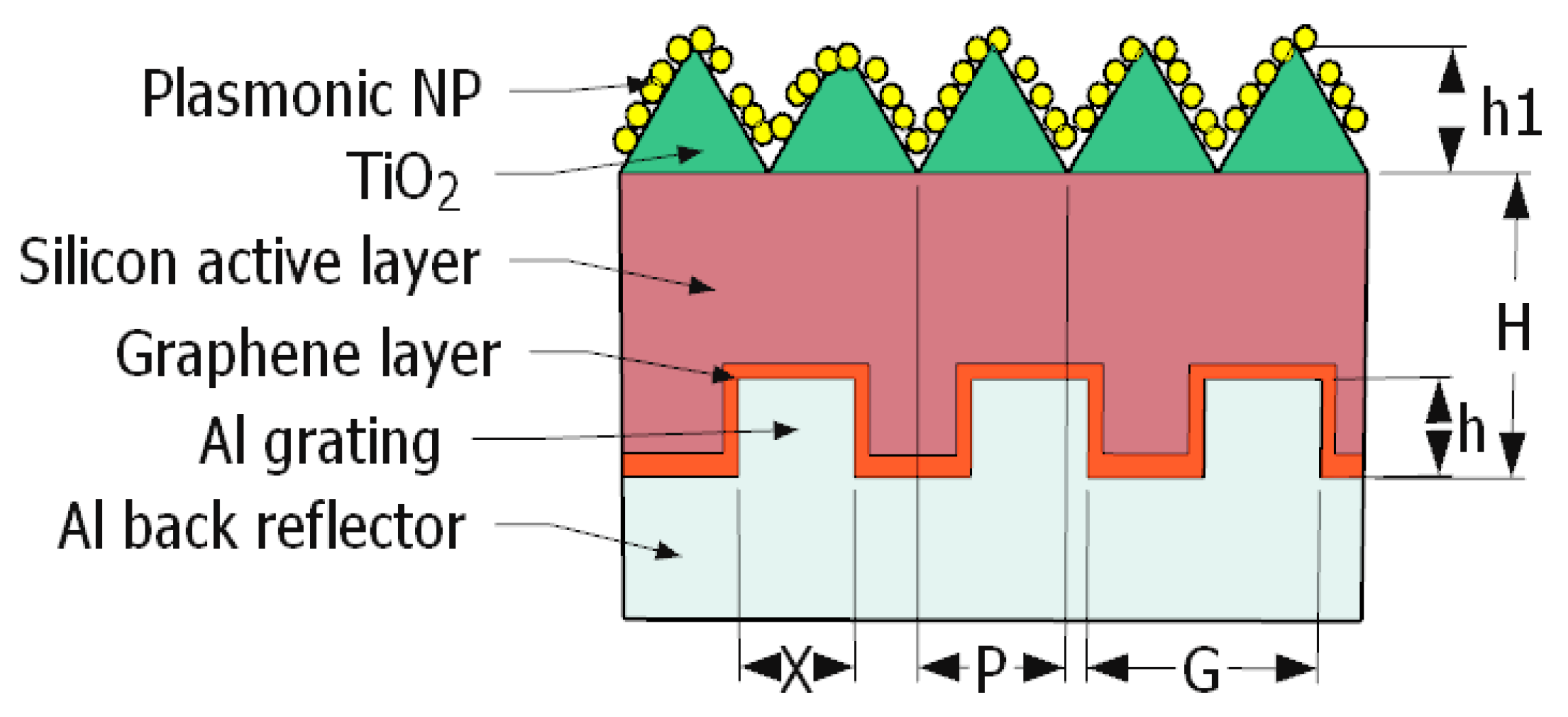
3. Proposed Structure
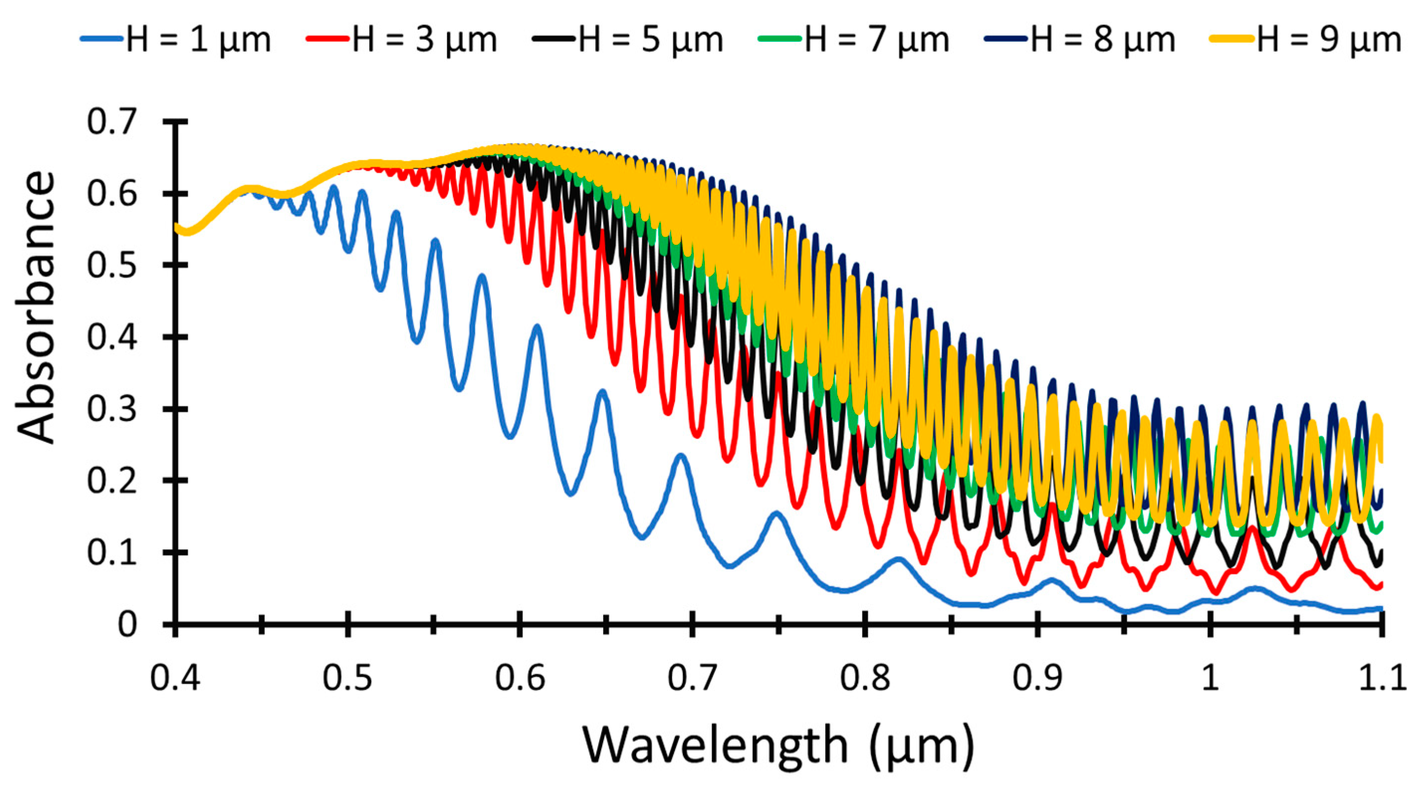
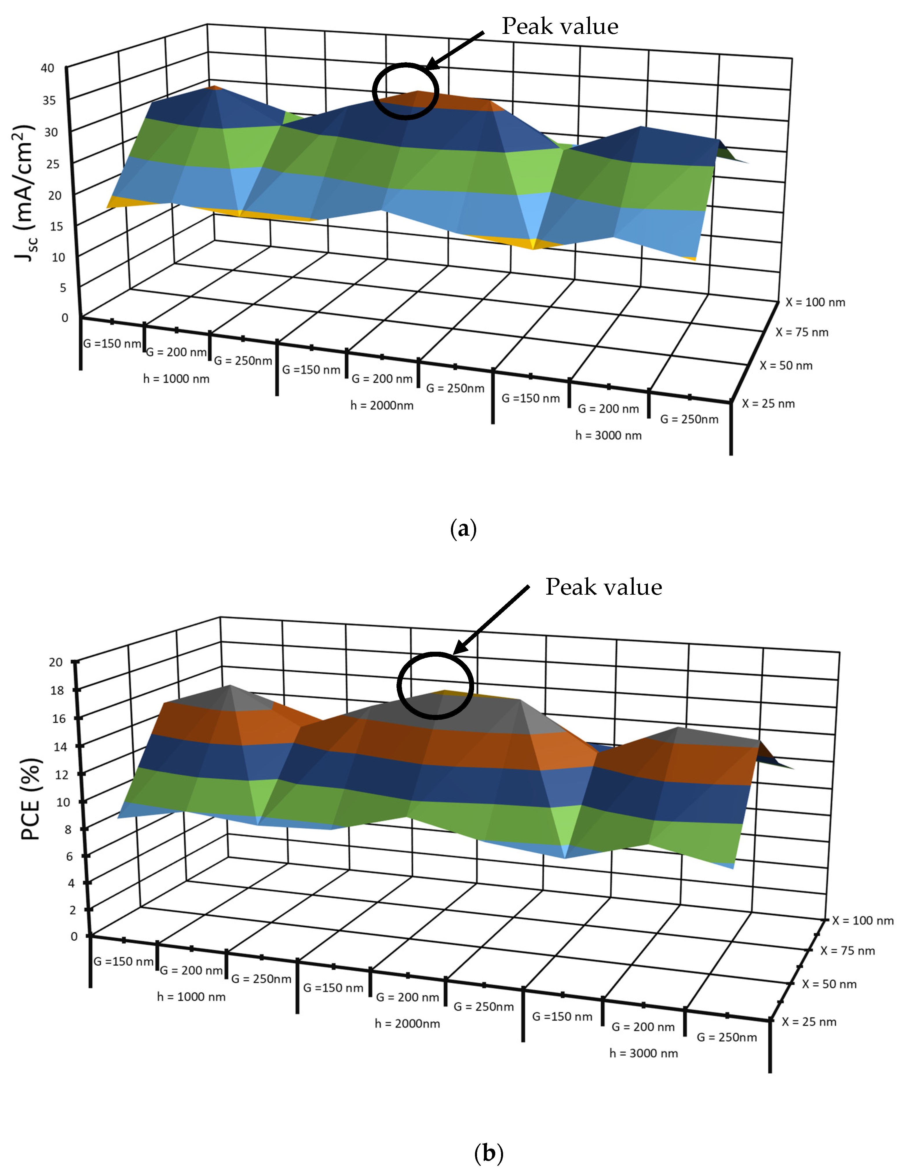
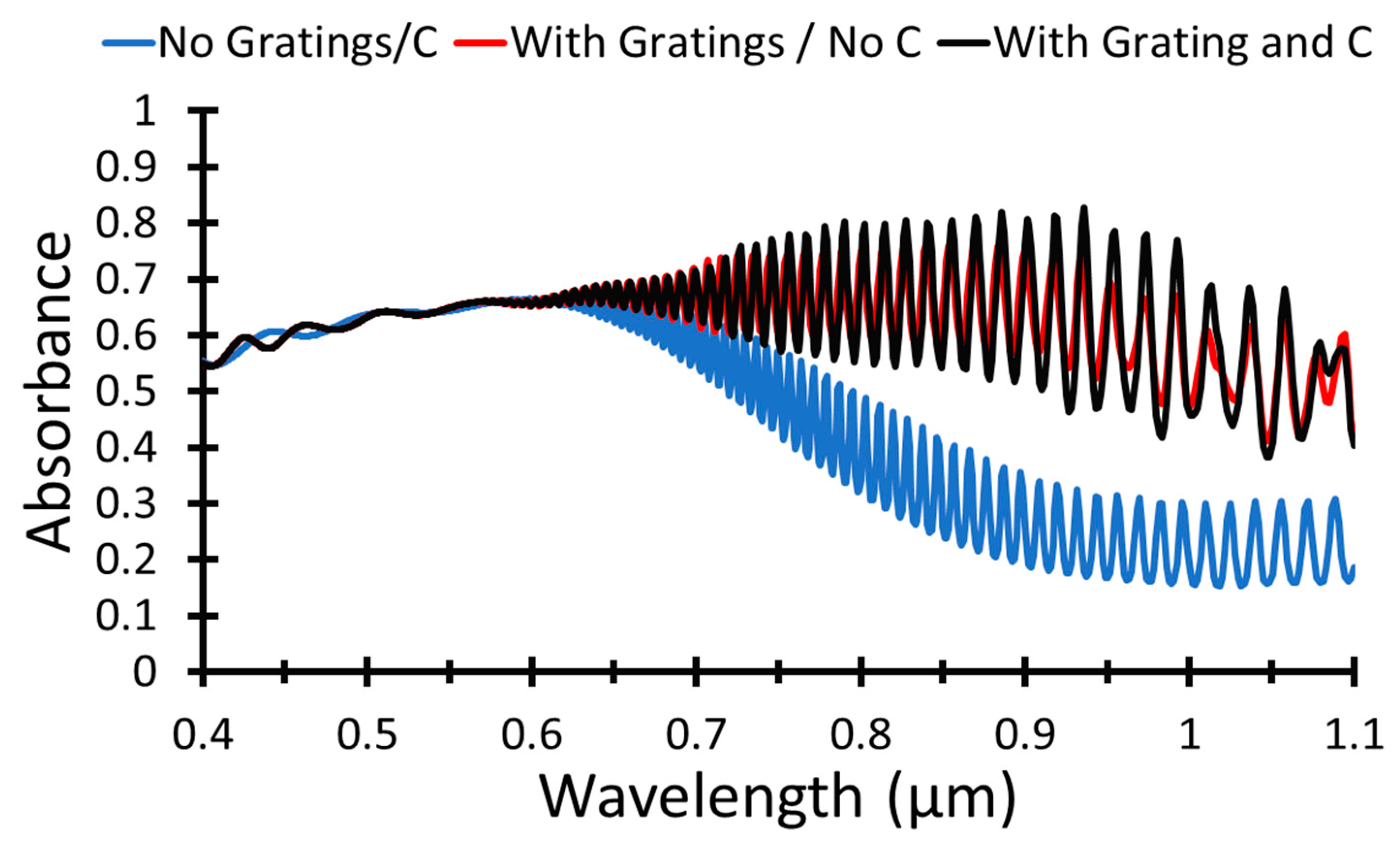
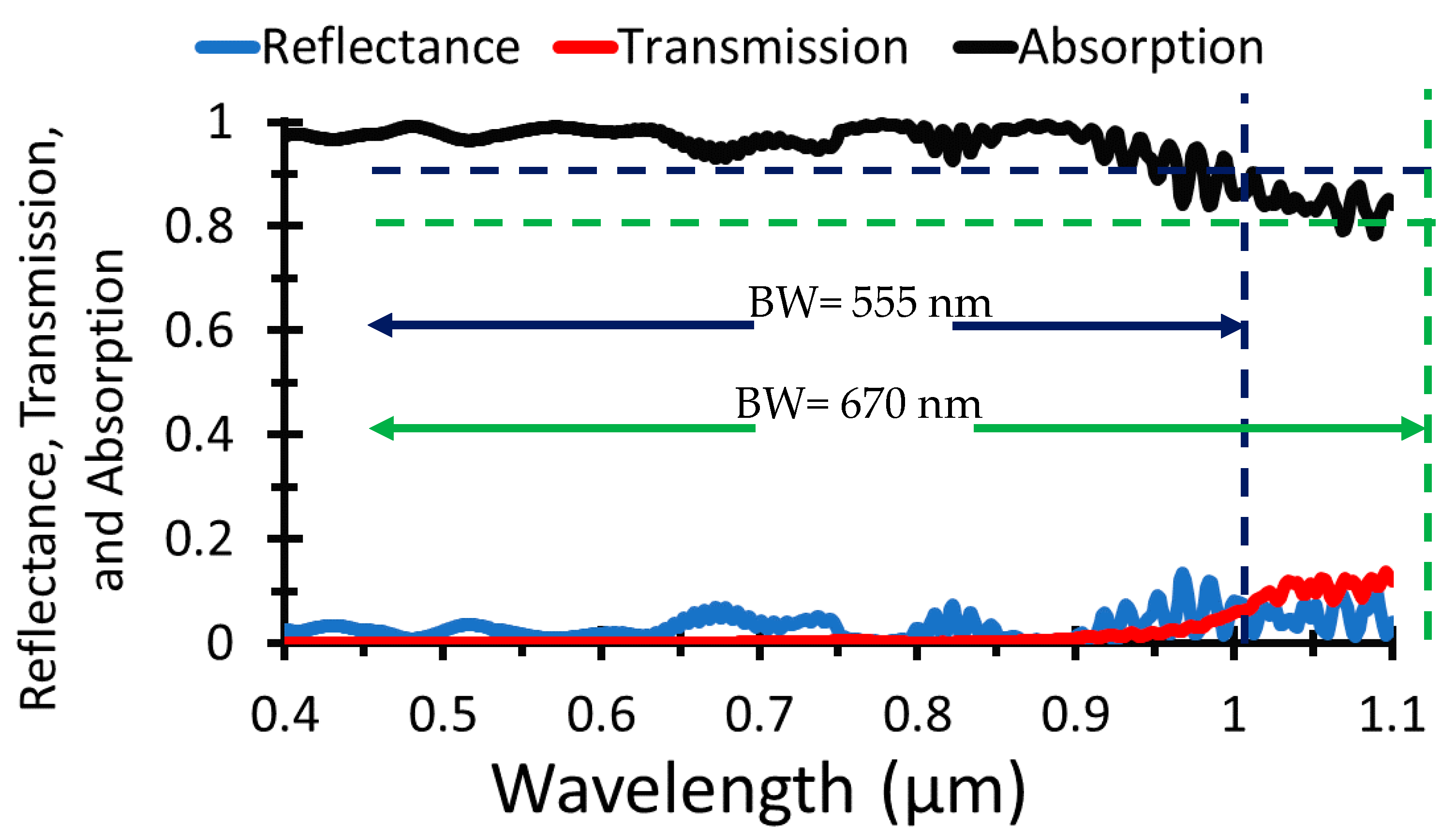
4. Results and Discussion
5. Conclusions
Author Contributions
Funding
Institutional Review Board Statement
Informed Consent Statement
Data Availability Statement
Conflicts of Interest
References
- Tu, Y.; Wang, S.; Wu, C.; Chang, K.; Lin, T.; Hung, C.; Wu, J. Improving Crystalline Silicon Solar Cell Efficiency Using Graded-Refractive-Index SiON/ZnO Nanostructures. Int. J. Photoenergy 2015, 2015, 275697. [Google Scholar] [CrossRef] [Green Version]
- Pham, D.; Yi, J. Dopant-grading proposal for polysilicon passivating contact in crystalline silicon solar cells. J. Power Sources 2022, 522, 231005. [Google Scholar] [CrossRef]
- Shockley, W.; Queisser, H. Detailed balance limit of efficiency of p-n junction solar cells. J. Appl. Phys. 1961, 32, 510–519. [Google Scholar] [CrossRef]
- Yu, L.; Cabarrocas, P. Polymorphous nano-si and radial junction solar cells. In Handbook of Photovoltaic Silicon; Springer: Berlin/Heidelberg, Germany, 2018. [Google Scholar]
- Street, R.; Qi, P.; Lujan, R.; Wong, W. Reflectivity of disordered silicon nanowires. Appl. Phys. Lett. 2008, 93, 163109. [Google Scholar] [CrossRef]
- Street, R.; Wong, W.; Paulson, C. Analytic model for diffuse reflectivity of silicon nanowire mats. Nano Lett. 2009, 9, 3494–3497. [Google Scholar] [CrossRef] [PubMed]
- Brönstrup, G.; Jahr, N.; Leiterer, C.; Csáki, A.; Fritzsche, W.; Christiansen, S. Optical properties of individual silicon nanowires for photonic devices. ACS Nano 2010, 4, 7113–7122. [Google Scholar] [CrossRef] [PubMed]
- Wallace, S.; Jevasuwan, W.; Fukata, N. Silicon nanowires covered with on-site fabricated nanowire-shape graphene for schottky junction solar cells. Sol. Energy 2021, 224, 666–671. [Google Scholar] [CrossRef]
- Li, X.; Zhu, H.; Wang, K.; Cao, A.; Wei, J.; Li, C.; Jia, Y.; Li, Z.; Li, X.; Wu, D. Graphene-on-silicon Schottky junction solar cells. Adv. Mater. 2010, 22, 2743–2748. [Google Scholar] [CrossRef]
- Liu, X.; Zhang, W.; Meng, H.; Yin, G.; Zhang, Q.; Wang, L.; Wu, L. High-efficiency schottky junction solar cells by co-doping of graphene with gold nanoparticles and nitric acid. Appl. Phys. Lett. 2015, 106, 233901. [Google Scholar] [CrossRef]
- Lee, C.; Lu, M.; Guan, Q.; Tung, Y.; Tsai, S.; Lin, F. Thickness-controllable textured TiO2 underlayer for a flexible dye-sensitized solar cell sub-module. Mater. Res. Express 2014, 1, 025503. [Google Scholar] [CrossRef]
- Barbe, J.; Thomson, F.; Wang, E.; McIntosh, K.; Catchpole, K. Nanoimprinted TiO2 Sol—Gel passivating diffraction gratings for solar cell applications. Prog. Photovolt. Res. Appl. 2012, 20, 143–148. [Google Scholar] [CrossRef]
- Elrashidi, A. Electrophotonic improvement of polymer solar cells by using graphene and plasmonic nanoparticles. Mater. Express 2017, 7, 1–7. [Google Scholar] [CrossRef]
- Huang, Y.; Liang, H.; Zhang, Y.; Yin, S.; Cai, C.; Liu, W.; Jia, T. Vertical tip-to-tip interconnection p–n silicon nanowires for plasmonic hot electron-enhanced broadband photodetectors. ACS Appl. Nano Mater. 2021, 4, 1567–1575. [Google Scholar] [CrossRef]
- Jbira, E.; Derouiche, H.; Missaoui, K. Enhancing effect of silver nanoparticles (AgNPs) interfacial thin layer on silicon nanowires (SiNWs)/PEDOT: PSS hybrid solar cell. Sol. Energy 2020, 211, 1230–1238. [Google Scholar] [CrossRef]
- Zhou, F.; Qin, F.; Yi, Z.; Yao, W.; Liu, Z.; Wu, X.; Wu, P. Ultra-wideband and wide-angle perfect solar energy absorber based on Ti nanorings surface plasmon resonance. Phys. Chem. Chem. Phys. 2021, 23, 17041–17048. [Google Scholar] [CrossRef]
- Deng, Y.; Cao, G.; Wu, Y.; Zhou, X.; Liao, W. Theoretical Description of Dynamic Transmission Characteristics in MDM Waveguide Aperture-Side-Coupled with Ring Cavity. Plasmonics 2015, 10, 1537–1543. [Google Scholar] [CrossRef]
- Deng, Y.; Cao, G.; Yang, H.; Zhou, X.; Wu, Y. Dynamic Control of Double Plasmon-Induced Transparencies in Aperture-Coupled Waveguide-Cavity System. Plasmonics 2018, 13, 345–352. [Google Scholar] [CrossRef]
- Zheng, Z.; Zheng, Y.; Luo, Y.; Yi, Z.; Zhang, J.; Liu, Z.; Yang, W.; Yu, Y.; Wu, X.; Wu, P. A switchable terahertz device combining ultra-wideband absorption and ultra-wideband complete reflection. Phys. Chem. Chem. Phys. 2022, 24, 2527–2533. [Google Scholar] [CrossRef]
- Zhao, F.; Lin, J.; Lei, Z.; Yi, Z.; Qin, F.; Zhang, J.; Liu, L.; Wu, X.; Yang, W.; Wu, P. Realization of 18.97% theoretical efficiency of 0.9 μm thick c-Si/ZnO heterojunction ultrathin-film solar cells via surface plasmon resonance enhancement. Phys. Chem. Chem. Phys. 2022, 24, 4871–4880. [Google Scholar] [CrossRef] [PubMed]
- Yang, X.; Wang, D. Photocatalysis: From Fundamental Principles to Materials and Applications. ACS Appl. Energy Mater. 2018, 1, 6657–6693. [Google Scholar] [CrossRef]
- Nan, T.; Zeng, H.; Liang, W.; Liu, S.; Wang, Z.; Huang, W.; Yang, W.; Chen, C.; Lin, Y. Growth Behavior and Photoluminescence Properties of ZnO Nanowires on Gold nanoparticle Coated Si Surfaces. J. Cryst. Growth 2012, 340, 83–86. [Google Scholar] [CrossRef]
- Kang, Z.; Gu, S.; Yan, Q.; Bai, M.; Liu, H.; Liu, S.; Zhang, H.; Zhang, Z.; Zhang, J.; Zhang, Y. Enhanced Photoelectrochemical Property of ZnO Nanorods Array Synthesized on Reduced Graphene Oxide for Self-powered Biosensing Application. Biosen. Bioelectron. 2015, 64, 499–504. [Google Scholar] [CrossRef] [PubMed]
- Kang, Z.; Yan, Q.; Wang, F.; Bai, M.; Liu, C.; Zhang, Z.; Lin, P.; Zhang, H.; Yuan, G.; Zhang, J.; et al. Electronic Structure Engineering of Cu2O Film/ZnO Nanorods Array All-oxide p-n Heterostructure for Enhanced Photoelectrochemical Property and Self-powered Biosensing Application. Sci. Rep. 2015, 5, 7882. [Google Scholar] [CrossRef] [Green Version]
- Garnett, E.; Yang, P. Light trapping in silicon nanowire solar cells. Nano Lett. 2010, 10, 1082–1087. [Google Scholar] [CrossRef] [PubMed]
- Yoon, J.; Baca, A.; Park, S.; Elvikis, P.; Geddes, J.; Li, L.; Kim, R.; Xiao, J.; Wang, S.; Kim, T.; et al. Ultrathin silicon solar microcells for semitransparent, mechanically flexible and microconcentrator module designs. Nat. Mater. 2008, 7, 907–915. [Google Scholar] [CrossRef] [PubMed]
- Augusto, A.; Herasimenka, S.; King, R.; Bowden, S.; Honsberg, C. Analysis of the recombination mechanisms of a silicon solar cell with low bandgap-voltage offset. J. Appl. Phys. 2017, 121, 205704. [Google Scholar] [CrossRef]
- Chong, T.; Wilson, J.; Mokkapati, S.; Catchpole, K. Optimal wavelength scale diffraction gratings for light trapping in solar cells. J. Opt. 2012, 14, 024012. [Google Scholar] [CrossRef] [Green Version]
- Dimitrov, D.; Du, C. Crystalline silicon solar cells with micro/nano texture. Appl. Surf. Sci. 2013, 266, 1–4. [Google Scholar] [CrossRef]
- Zhang, D.; Wang, L.; Jia, R.; Tao, K.; Jiang, S.; Ge, H.; Wang, B.; Gao, Z.; Li, X.; Li, M.; et al. Improving the performance of PERC silicon solar cells by optimizing the surface inverted pyramid structure on large-area mono-crystalline silicon wafers. Mater. Sci. Semicond. Process. 2022, 138, 106281. [Google Scholar] [CrossRef]
- Elrashidi, A. Light Harvesting in Silicon Nanowires Solar Cells by Using Graphene Layer and Plasmonic Nanoparticles. Appl. Sci. 2022, 12, 2519. [Google Scholar] [CrossRef]
- Khokhar, M.; Hussain, S.; Chowdhury, S.; Zahid, M.; Pham, D.; Jeong, S.; Kim, S.; Kim, S.; Cho, E.; Yi, J. High-efficiency hybrid solar cell with a nano-crystalline silicon oxide layer as an electron-selective contact. Energy Convers. Manag. 2022, 252, 115033. [Google Scholar] [CrossRef]
- Sinton, R.; Cuevas, A. Contactless determination of current–voltage characteristics and minority-carrier lifetimes in semiconductors from quasi-steady-state photoconductance data. Appl. Phys. Lett. 1996, 69, 2510. [Google Scholar] [CrossRef]
- Devore, J. Refractive indices of rutile and sphalerite. J. Opt. Soc. Am. 1951, 41, 416–419. [Google Scholar] [CrossRef]
- Aspnes, D.; Studna, A. Dielectric functions and optical parameters of Si, Ge, GaP, GaAs, GaSb, InP, InAs, and InSb from 1.5 to 6.0 eV. Phys. Rev. 1983, 27, 985. [Google Scholar] [CrossRef]
- Phillip, H.; Taft, E. Kramers-Kronig Analysis of Reflectance Data for Diamond. Phys. Rev. 1964, 136, A1445. [Google Scholar] [CrossRef]
- Elrashidi, A.; Tharwat, M. Broadband absorber using ultra-thin plasmonic metamaterials nanostructure in the visible and near-infrared regions. Opt. Quantum Electron. 2021, 53, 426. [Google Scholar] [CrossRef]


| Material | Term (k) | Damping Constant | Plasma Frequency (Hz) | Resonant Frequency (Hz) | Damping Frequency (Hz) |
|---|---|---|---|---|---|
| Ag | 0 | 0.8450 | 0.136884 × 10¹⁷ | 0.000000 × 1000 | 0.729239 × 10¹⁴ |
| 1 | 0.0650 | 0.136884 × 10¹⁷ | 0.123971 × 10¹⁶ | 0.590380 × 10¹⁶ | |
| 2 | 0.1240 | 0.136884 × 10¹⁷ | 0.680775 × 10¹⁶ | 0.686701 × 10¹⁵ | |
| 3 | 0.0110 | 0.136884 × 10¹⁷ | 0.124351 × 10¹⁷ | 0.987512 × 10¹⁴ | |
| 4 | 0.8400 | 0.136884 × 10¹⁷ | 0.137993 × 10¹⁷ | 0.139163 × 10¹⁶ | |
| 5 | 5.6460 | 0.136884 × 10¹⁷ | 0.308256 × 10¹⁷ | 0.367506 × 10¹⁶ | |
| Au | 0 | 0.7600 | 0.137188 × 10¹⁷ | 0.000000 × 1000 | 0.805202 × 10¹⁴ |
| 1 | 0.0240 | 0.137188 × 10¹⁷ | 0.630488 × 10¹⁵ | 0.366139 × 10¹⁵ | |
| 2 | 0.0100 | 0.137188 × 10¹⁷ | 0.126098 × 10¹⁶ | 0.524141 × 10¹⁵ | |
| 3 | 0.0710 | 0.137188 × 10¹⁷ | 0.451065 × 10¹⁶ | 0.132175 × 10¹⁶ | |
| 4 | 0.6010 | 0.137188 × 10¹⁷ | 0.653885 × 10¹⁶ | 0.378901 × 10¹⁶ | |
| 5 | 4.3840 | 0.137188 × 10¹⁷ | 0.202364 × 10¹⁷ | 0.336362 × 10¹⁶ | |
| Cu | 0 | 0.5750 | 0.164535 × 10¹⁷ | 0.000000 × 1000 | 0.455775 × 10¹⁴ |
| 1 | 0.0610 | 0.164535 × 10¹⁷ | 0.442101 × 10¹⁵ | 0.574276 × 10¹⁵ | |
| 2 | 0.1040 | 0.164535 × 10¹⁷ | 0.449242 × 10¹⁶ | 0.160433 × 10¹⁶ | |
| 3 | 0.7230 | 0.164535 × 10¹⁷ | 0.805202 × 10¹⁶ | 0.488135 × 10¹⁶ | |
| 4 | 0.6380 | 0.164535 × 10¹⁷ | 0.169852 × 10¹⁷ | 0.654037 × 10¹⁶ | |
| Al | 0 | 0.5230 | 0.227583 × 10¹⁷ | 0.000000 × 1000 | 0.714047 × 10¹⁴ |
| 1 | 0.2270 | 0.227583 × 10¹⁷ | 0.246118 × 10¹⁵ | 0.505910 × 10¹⁵ | |
| 2 | 0.0500 | 0.227583 × 10¹⁷ | 0.234572 × 10¹⁶ | 0.474006 × 10¹⁵ | |
| 3 | 0.1660 | 0.227583 × 10¹⁷ | 0.274680 × 10¹⁶ | 0.205251 × 10¹⁶ | |
| 4 | 0.0300 | 0.227583 × 10¹⁷ | 0.527635 × 10¹⁶ | 0.513810 × 10¹⁶ |
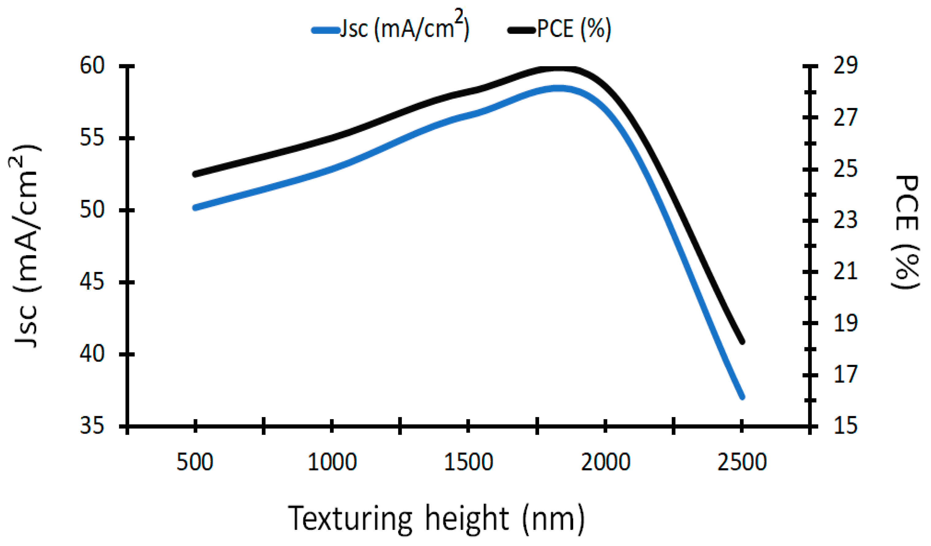
| H (µm) | Jsc (mA/cm2) | PCE (%) |
|---|---|---|
| 1 | 8.9 | 4.4 |
| 2 | 11.94 | 5.9 |
| 3 | 13.6 | 6.7 |
| 4 | 15.5 | 7.7 |
| 5 | 16.1 | 7.9 |
| 6 | 17.1 | 8.4 |
| 7 | 17.3 | 8.6 |
| 8 | 18.8 | 9.3 |
| 9 | 18.1 | 9.0 |
| X = 25 nm | X = 50 nm | X = 75 nm | X = 100 nm | ||||||
|---|---|---|---|---|---|---|---|---|---|
| h (nm) | G (nm) | Jsc (mA/cm2) | PCE (%) | Jsc (mA/cm2) | PCE (%) | Jsc (mA/cm2) | PCE (%) | Jsc (mA/cm2) | PCE (%) |
| 1000 | 150 | 18.4 | 9 | 32.1 | 15.9 | 26.2 | 13 | 20.9 | 10.3 |
| 200 | 20.3 | 10 | 35.6 | 17.6 | 28.2 | 14 | 23.1 | 11.4 | |
| 250 | 19.2 | 9.5 | 30.1 | 14.9 | 27.1 | 13.4 | 21.6 | 10.7 | |
| 2000 | 150 | 19.6 | 9.7 | 33.9 | 16.8 | 26.01 | 12.9 | 22 | 10.9 |
| 200 | 22.4 | 11.1 | 37.07 | 18.3 | 28.7 | 14.2 | 24.19 | 12 | |
| 250 | 20.1 | 9.9 | 36.4 | 18 | 27.1 | 13.9 | 23.3 | 11.5 | |
| 3000 | 150 | 18.8 | 9.3 | 29.7 | 14.7 | 24.36 | 12.1 | 23.4 | 11.6 |
| 200 | 21.8 | 10.8 | 34.2 | 16.9 | 28 | 13.9 | 24.1 | 11.9 | |
| 250 | 19.6 | 9.7 | 33.1 | 16.4 | 26.8 | 13.3 | 22.6 | 11.2 | |
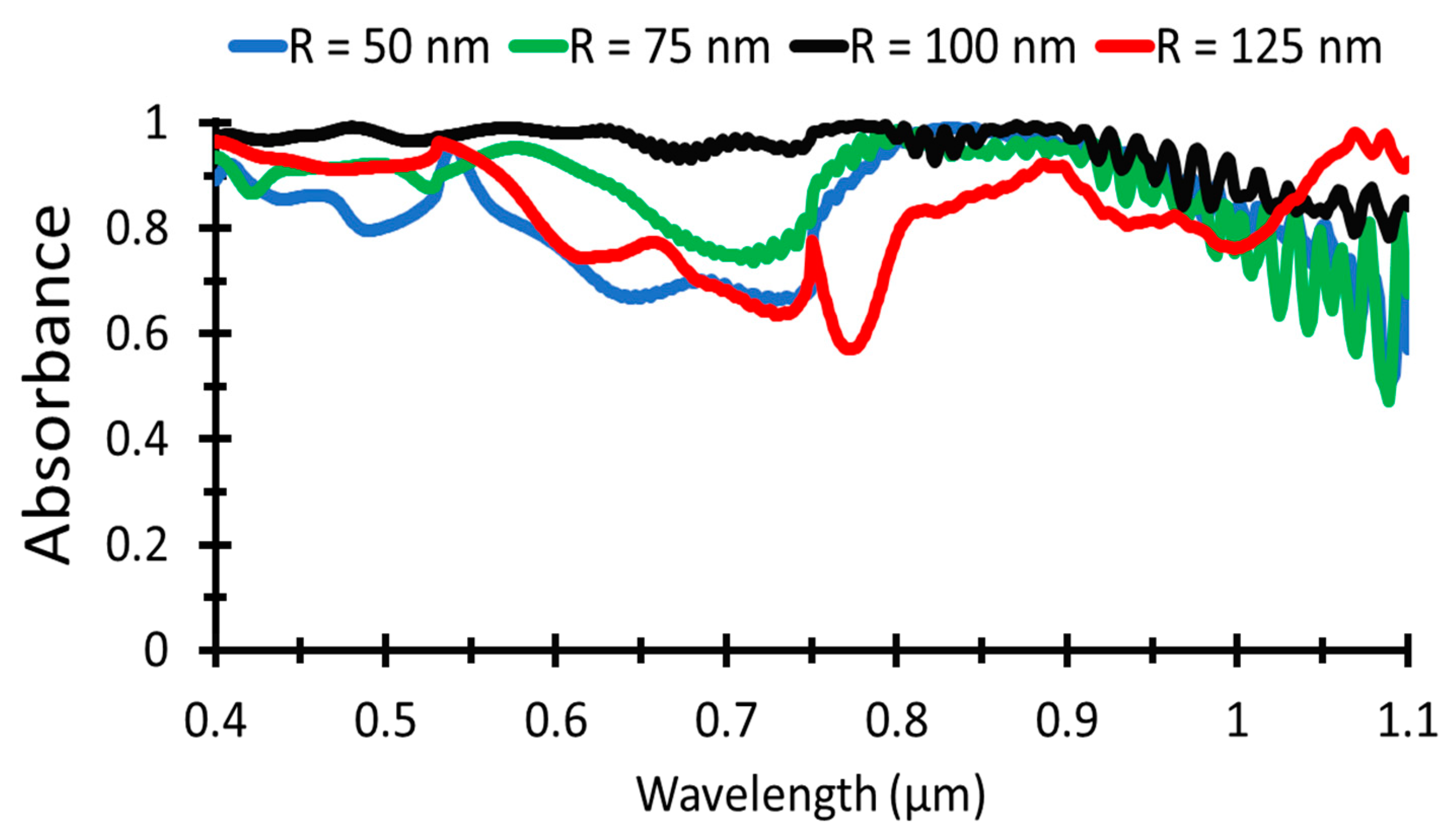
| R (nm) | Jsc (mA/cm2) | PCE (%) |
|---|---|---|
| 50 | 39.8 | 19.7 |
| 75 | 45.8 | 22.7 |
| 100 | 61.9 | 30.6 |
| 125 | 35.5 | 17.6 |
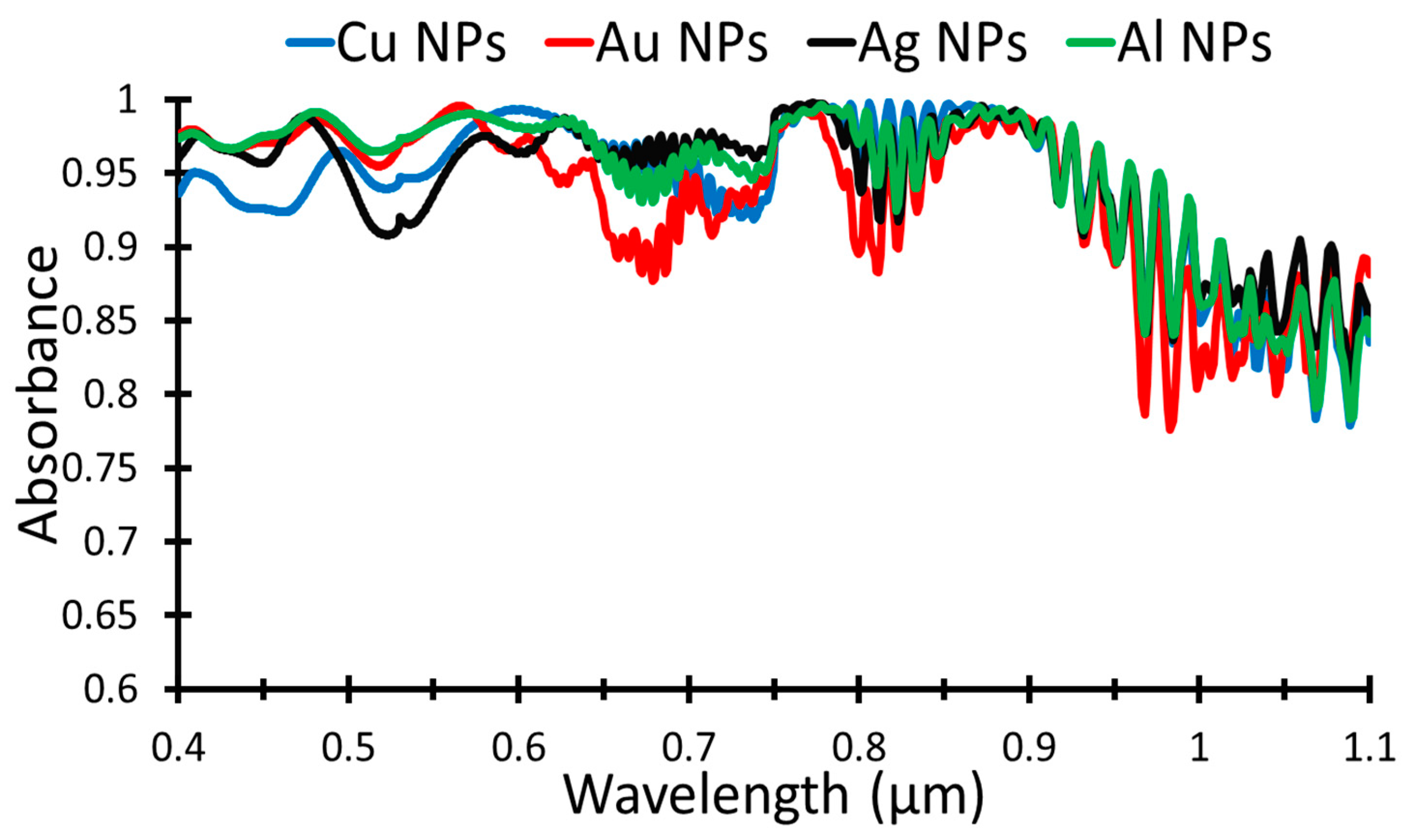
| Plasmonic Material | Jsc (mA/cm2) | PCE (%) |
|---|---|---|
| Al | 61.9 | 30.6 |
| Au | 55.8 | 27.6 |
| Ag | 54.6 | 27.0 |
| Cu | 56.2 | 27.8 |
| Different Structure | Structure | Voc (V) | FF | Jsc (mA/cm2) | PCE (%) |
|---|---|---|---|---|---|
| [4] | SiNWs | 0.82 | 0.73 | 15.2 | 9.30 |
| [8] | SiNWs | 0.47 | 0.59 | 13.7 | 3.80 |
| [25] | SiNWs | 0.56 | 0.61 | 17.3 | 5.31 |
| [26] | Bulk Si | 0.51 | 0.61 | 33.6 | 11.61 |
| [27] | Bulk Si | 0.76 | 0.86 | 38.8 | - |
| [28] | Bulk Si (textured TiO2) | - | - | 33.4 | - |
| [29] | Textured Si | - | - | 35.5 | 17.50 |
| [30] | Inverted pyramid Si | 0.68 | 0.81 | 41.7 | 22.69 |
| [31] | SiNWs | 0.63 | 0.73 | 41.7 | 19.00 |
| [32] | a-Si:H | 0.72 | - | 38.95 | 21.4 |
| Proposed structure | Texturing Tio2 Al NPs Al gratings | 0.60 | 0.83 | 61.9 | 30.6 |
Publisher’s Note: MDPI stays neutral with regard to jurisdictional claims in published maps and institutional affiliations. |
© 2022 by the authors. Licensee MDPI, Basel, Switzerland. This article is an open access article distributed under the terms and conditions of the Creative Commons Attribution (CC BY) license (https://creativecommons.org/licenses/by/4.0/).
Share and Cite
Elrashidi, A.; Elleithy, K. High-Efficiency Crystalline Silicon-Based Solar Cells Using Textured TiO2 Layer and Plasmonic Nanoparticles. Nanomaterials 2022, 12, 1589. https://doi.org/10.3390/nano12091589
Elrashidi A, Elleithy K. High-Efficiency Crystalline Silicon-Based Solar Cells Using Textured TiO2 Layer and Plasmonic Nanoparticles. Nanomaterials. 2022; 12(9):1589. https://doi.org/10.3390/nano12091589
Chicago/Turabian StyleElrashidi, Ali, and Khaled Elleithy. 2022. "High-Efficiency Crystalline Silicon-Based Solar Cells Using Textured TiO2 Layer and Plasmonic Nanoparticles" Nanomaterials 12, no. 9: 1589. https://doi.org/10.3390/nano12091589