
3D Nanoprinting of All-Metal Nanoprobes for Electric AFM Modes
 , , , ,
Abstract
:1. Introduction
2. Methods
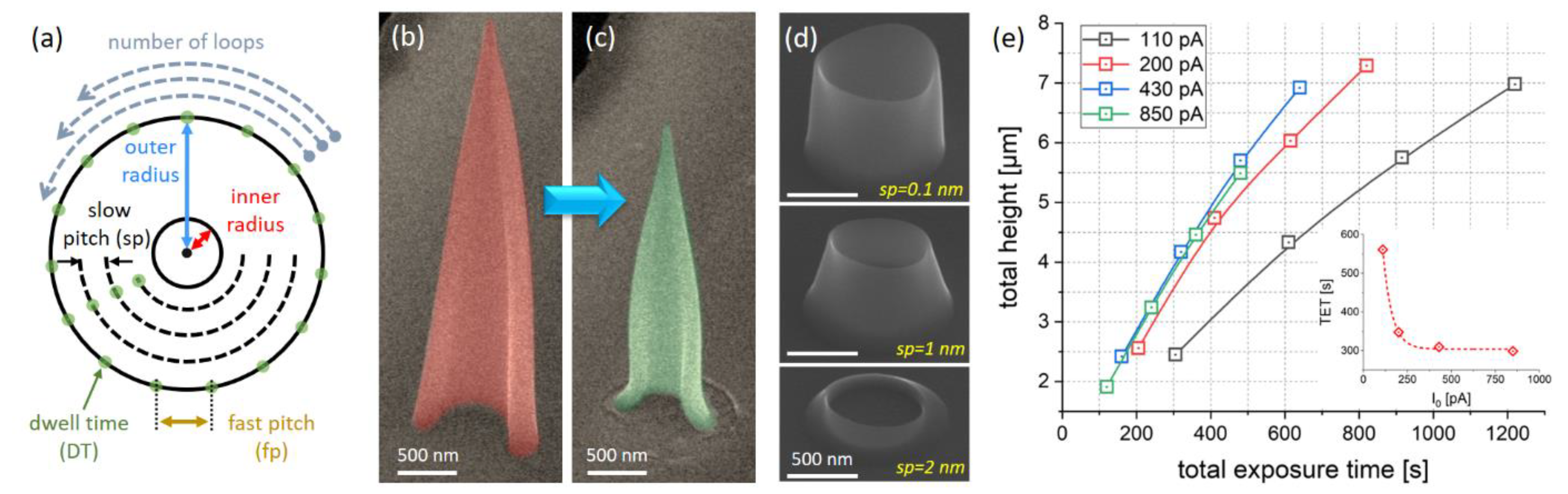
3. Hollow-Cone Fabrication
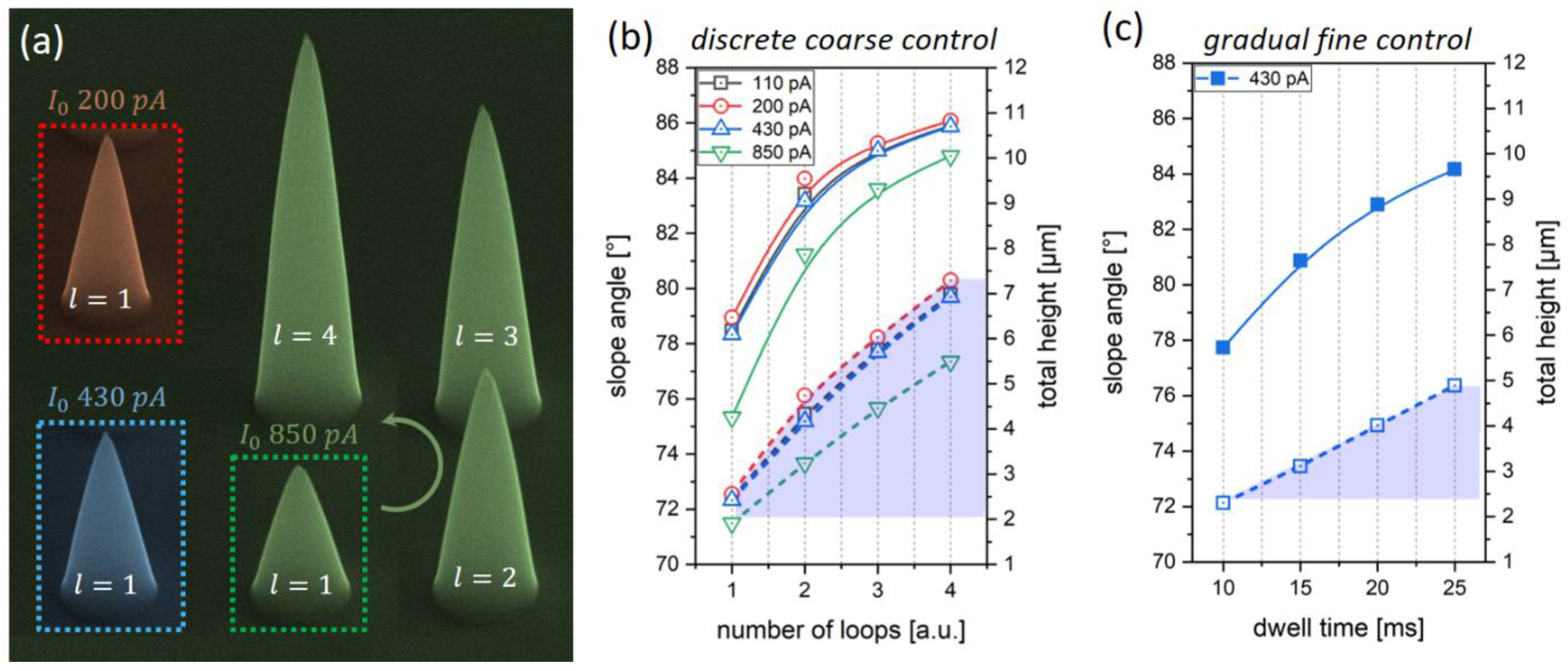
3.1. Hollow-Cone Deposition
3.2. Purification
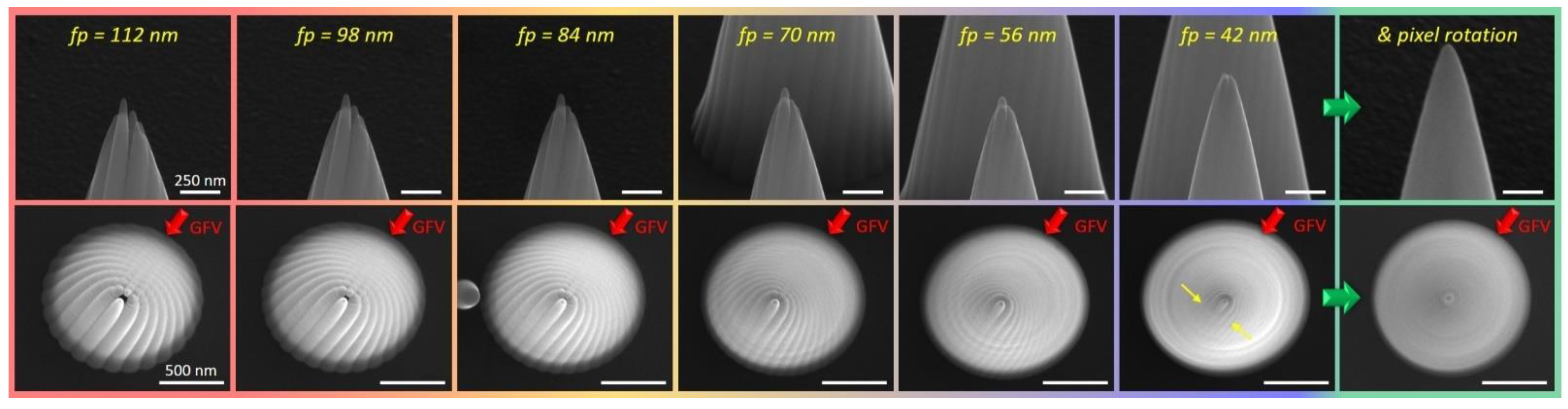
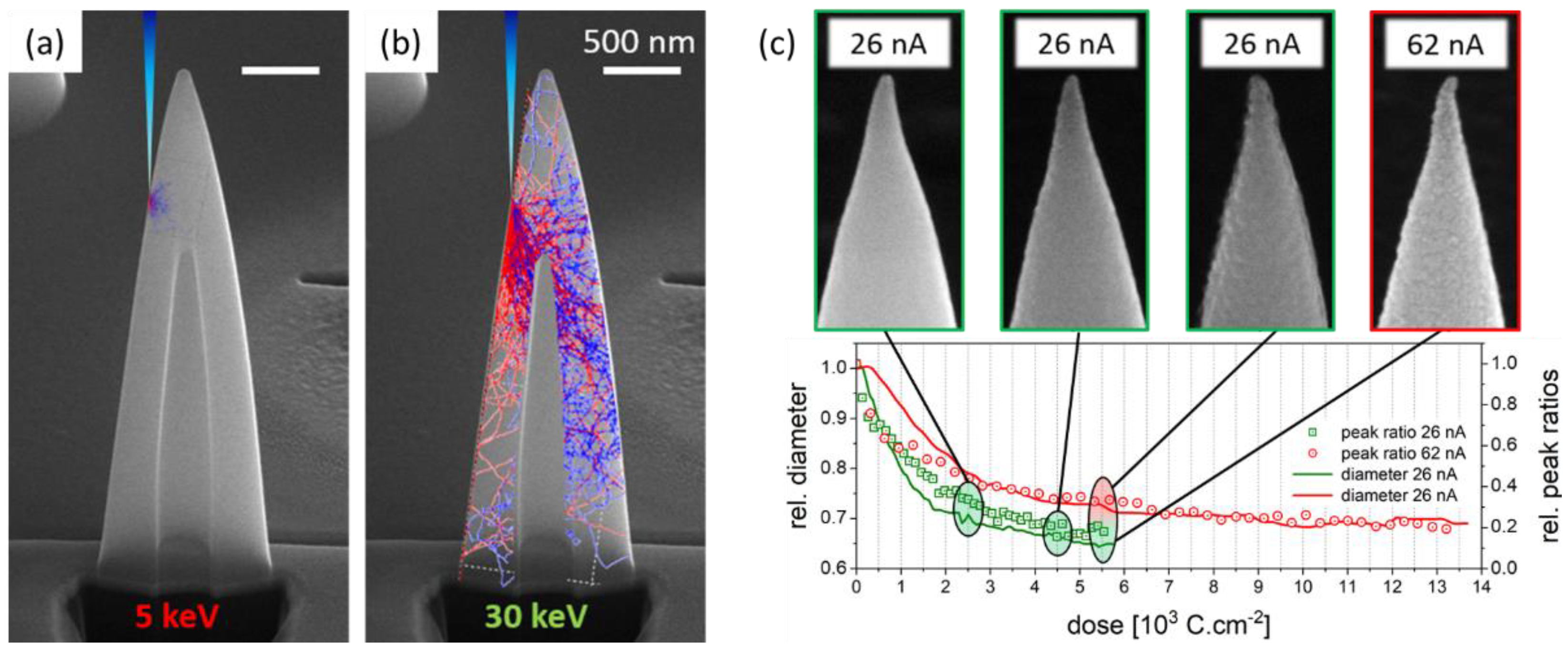
3.2.1. Beam Setup
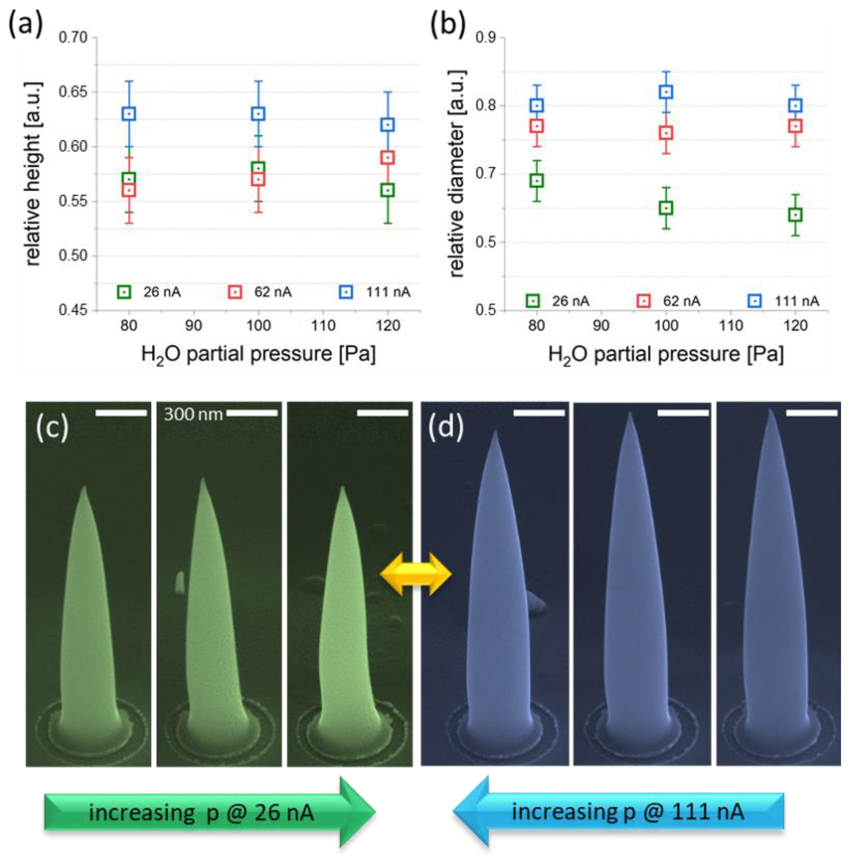
3.2.2. H2O Pressure
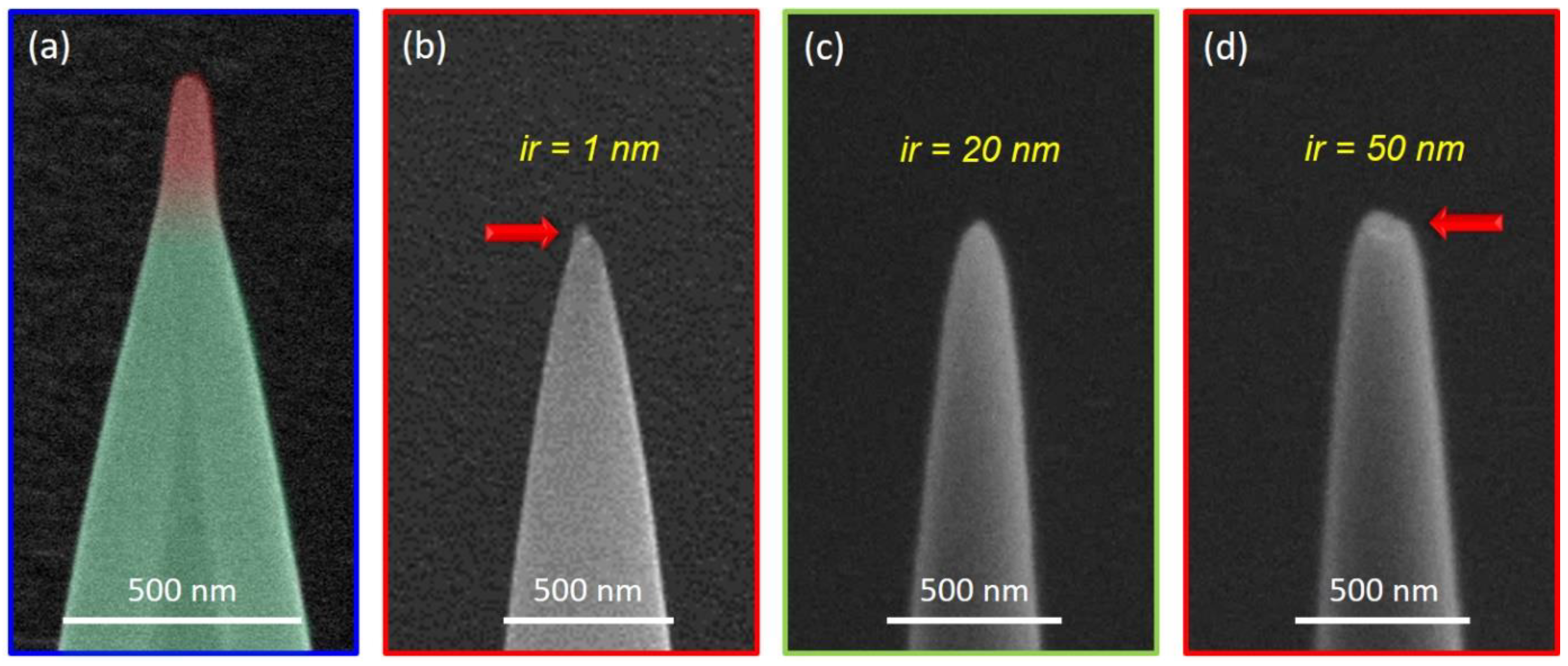
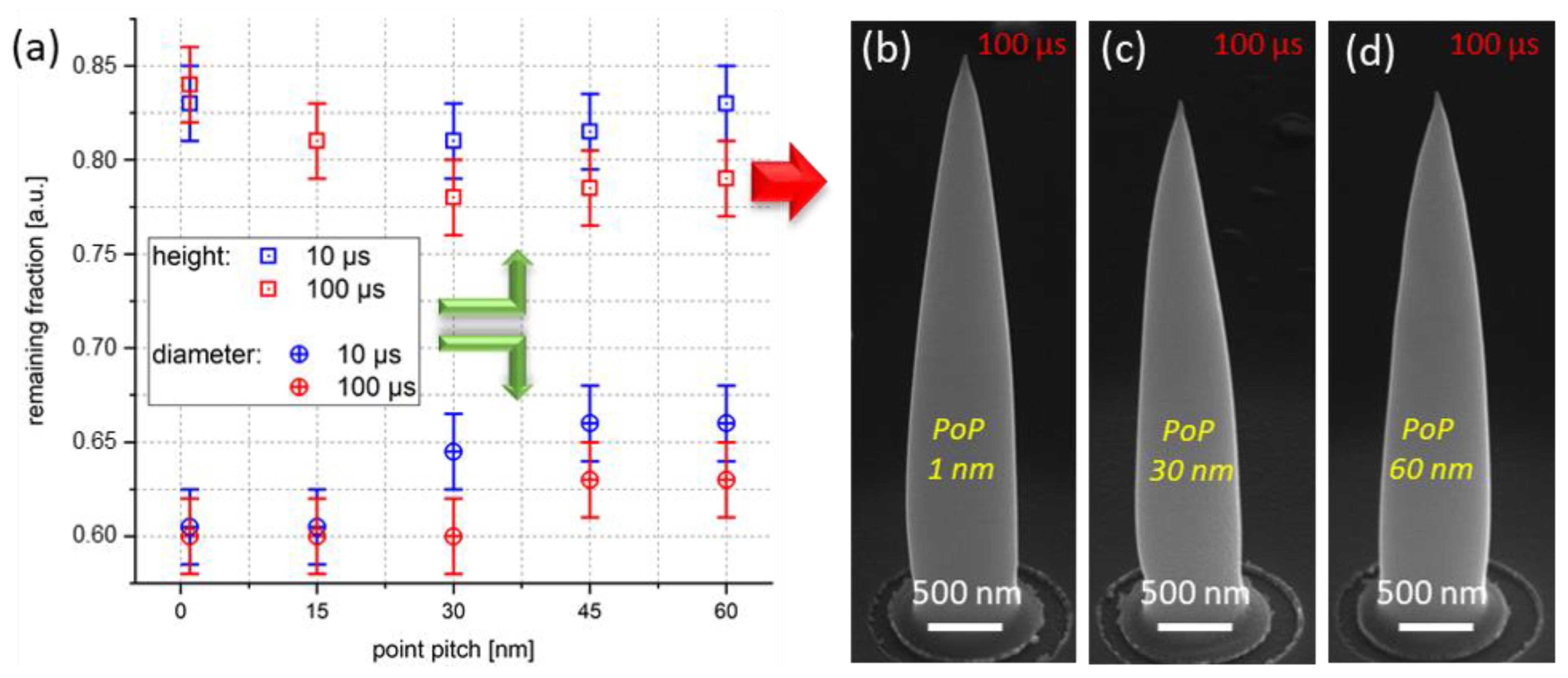
3.2.3. Purification Pattern
4. Characterization
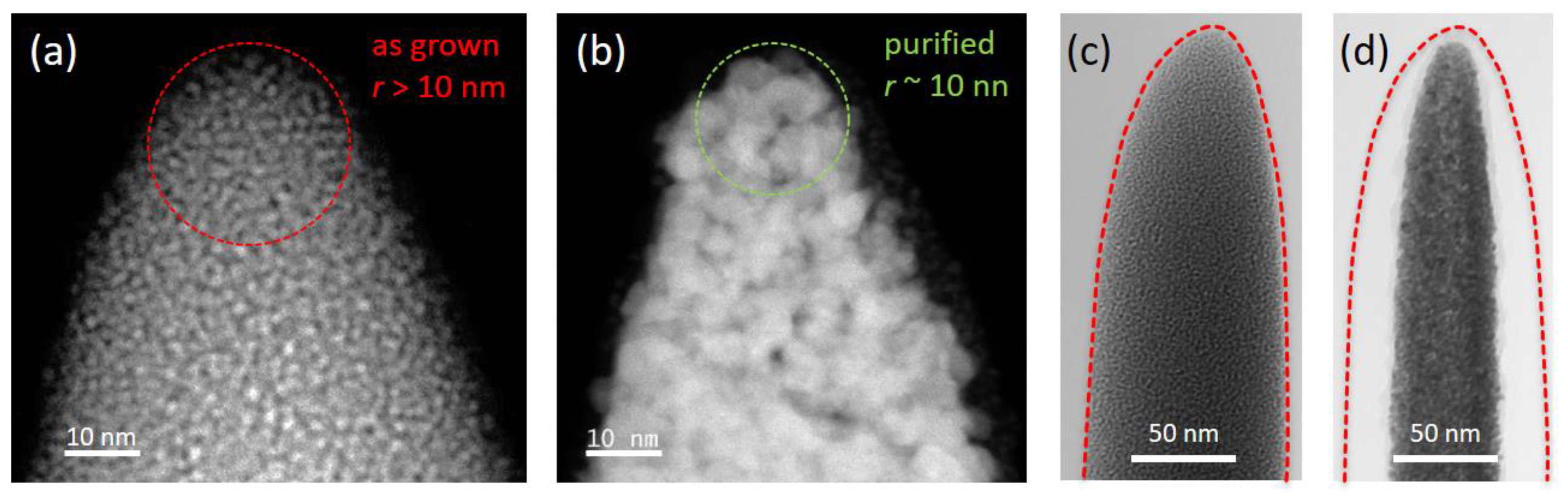
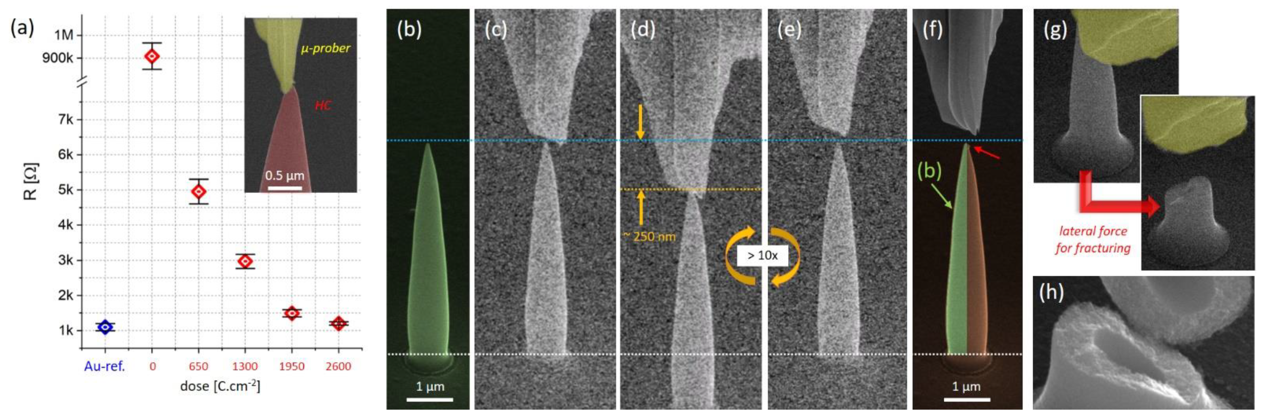
4.1. Strucural, Electrical and Mechanical Investigations
4.2. AFM Operation
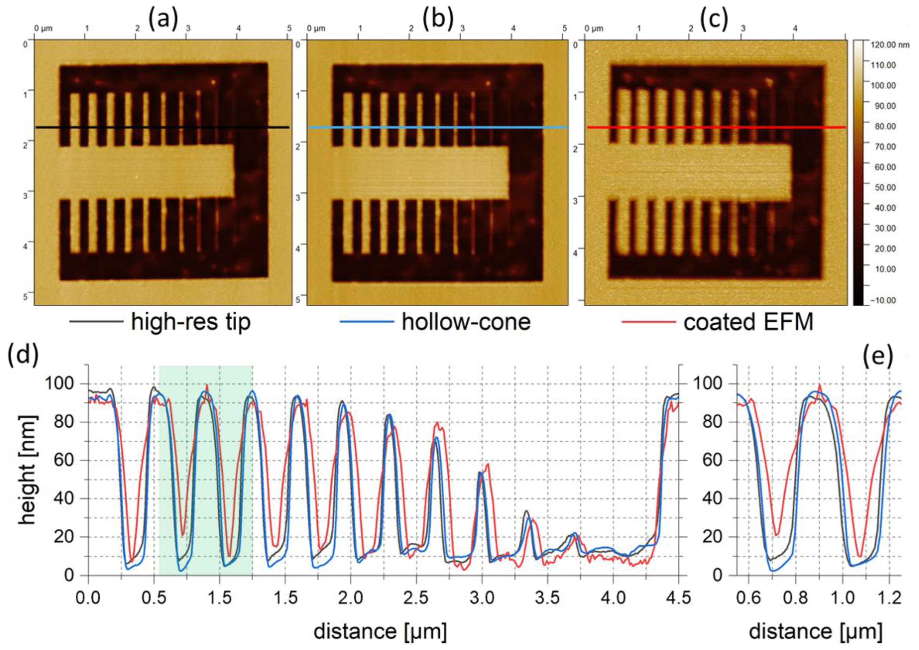
4.2.1. AFM Height
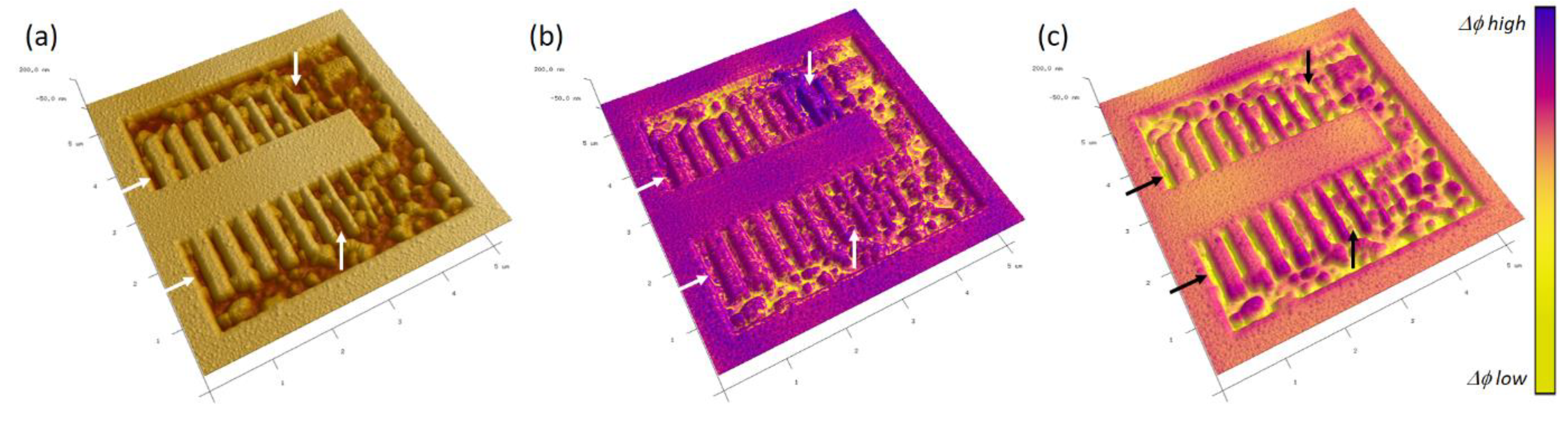
4.2.2. Electrostatic Force Microscopy
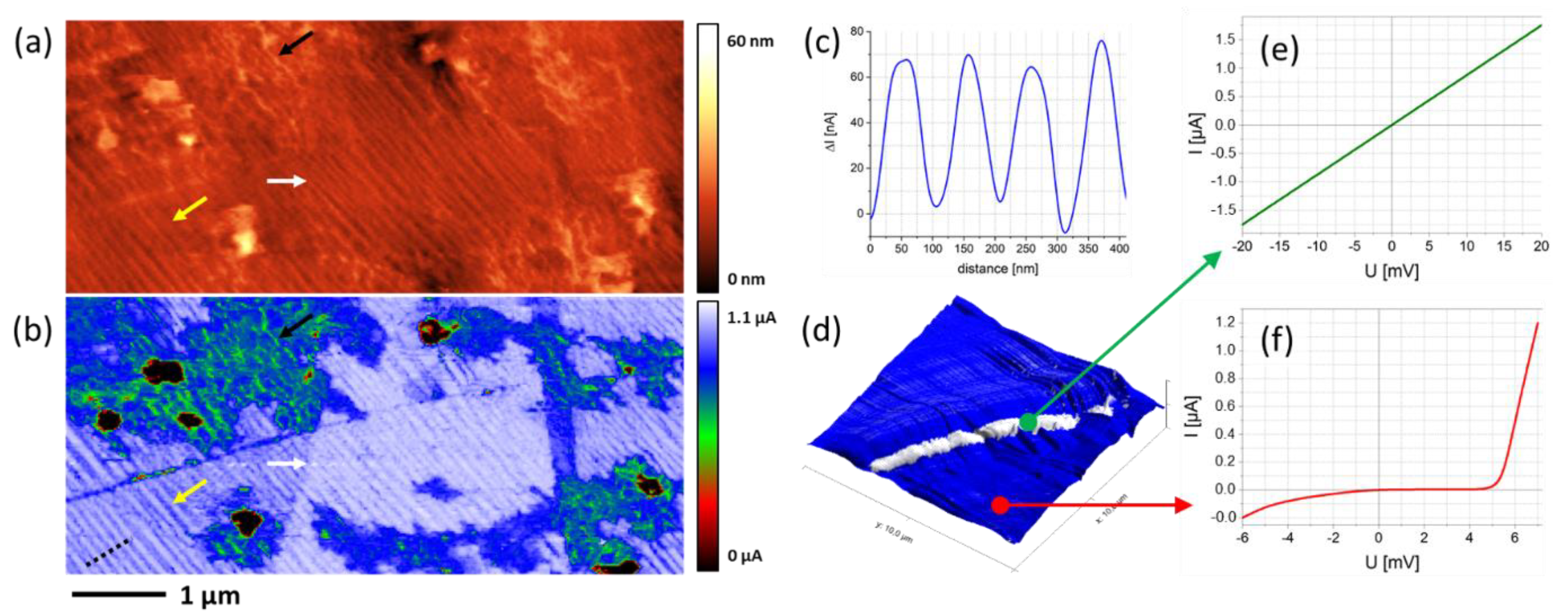
4.2.3. Conductive AFM
5. Conclusions
Author Contributions
Funding
Data Availability Statement
Acknowledgments
Conflicts of Interest
List of Abbreviations
| Abbreviation | Description | Unit |
| FEBID | Focused electron beam induced deposition | - - - |
| 3DNP | 3D Nanoprinting | - - - |
| HC | Hollow cone | - - - |
| AFM | Atomic force microscopy | - - - |
| EFM | Electrostatic force microscopy | - - - |
| CAFM | Conductive AFM | - - - |
| KFM | Kelvin force microscopy | - - - |
| SEM | Scanning electron microscope | - - - |
| FIB | Focused ion beam | - - - |
| DBM | Dual-beam microscope | - - - |
| STEM | Scanning transmission electron microscope | - - - |
| HAADF | High-angle annular dark field | - - - |
| EDXS | Energy-dispersive X-ray spectroscopy | - - - |
| PoP | Point pitch: distance between patterning pixels | nm |
| fp | Fast point pitch: PoP along pattern circumference | nm |
| sp | Slow point pitch: increment between successive circles | nm |
| DT | Dwell time: exposure at individual pixel points | ms |
| TET | Total exposure time: full patterning duration | s |
| VGR | Volume growth rate: timely normalized deposition volume (over tet) | nm3·s−1 |
References
- Voigtländer, B. Scanning Probe Microscopy; NanoScience and Technology; Springer: Berlin/Heidelberg, Germany, 2015; ISBN 978-3-662-45239-4. [Google Scholar]
- Tao, Z.; Bhushan, B. Surface modification of AFM silicon probes for adhesion and wear reduction. Tribol. Lett. 2006, 21, 1–16. [Google Scholar] [CrossRef]
- Bhaskaran, H.; Sebastian, A.; Despont, M. Nanoscale PtSi tips for conducting probe technologies. IEEE Trans. Nanotechnol. 2009, 8, 128–131. [Google Scholar] [CrossRef]
- Liu, J.; Grierson, D.S.; Moldovan, N.; Notbohm, J.; Li, S.; Jaroenapibal, P.; O’Connor, S.D.; Sumant, A.V.; Neelakantan, N.; Carlisle, J.A.; et al. Preventing nanoscale wear of atomic force microscopy tips through the use of monolithic ultrananocrystalline diamond probes. Small 2010, 6, 1140–1149. [Google Scholar] [CrossRef] [PubMed]
- Plank, H.; Winkler, R.; Schwalb, C.H.; Hütner, J.; Fowlkes, J.D.; Rack, P.D.; Utke, I.; Huth, M. Focused Electron Beam-Based 3D Nanoprinting for Scanning Probe Microscopy: A Review. Micromachines 2019, 11, 48. [Google Scholar] [CrossRef] [Green Version]
- Winkler, R.; Fowlkes, J.D.; Rack, P.D.; Plank, H. 3D nanoprinting via focused electron beams. J. Appl. Phys. 2019, 125, 210901. [Google Scholar] [CrossRef] [Green Version]
- Peinado, P.; Sangiao, S.; Teresa, J.M. De Focused Electron and Ion Beam Induced Deposition on Flexible and Transparent Polycarbonate Substrates. ACS Nano 2015, 9, 6139–6146. [Google Scholar] [CrossRef] [Green Version]
- Sattelkow, J.; Fröch, J.E.; Winkler, R.; Hummel, S.; Schwalb, C.; Plank, H. Three-Dimensional Nanothermistors for Thermal Probing. ACS Appl. Mater. Interfaces 2019, 11, 22655–22667. [Google Scholar] [CrossRef]
- Schwalb, C.H.; Grimm, C.; Baranowski, M.; Sachser, R.; Porrati, F.; Reith, H.; Das, P.; Müller, J.; Völklein, F.; Kaya, A.; et al. A Tunable Strain Sensor Using Nanogranular Metals. Sensors 2010, 10, 9847–9856. [Google Scholar] [CrossRef]
- Sachser, R.; Porrati, F.; Schwalb, C.H.; Huth, M. Universal Conductance Correction in a Tunable Strongly Coupled Nanogranular Metal. Phys. Rev. Lett. 2011, 107, 206803. [Google Scholar] [CrossRef]
- Trummer, C.; Winkler, R.; Plank, H.; Kothleitner, G.; Haberfehlner, G. Analyzing the Nanogranularity of Focused-Electron-Beam-Induced-Deposited Materials by Electron Tomography. ACS Appl. Nano Mater. 2019, 2, 5356–5359. [Google Scholar] [CrossRef]
- Kuhness, D.; Gruber, A.; Winkler, R.; Sattelkow, J.; Fitzek, H.; Letofsky-Papst, I.; Kothleitner, G.; Plank, H.; Letofsky-Pabst, I.; Kothleitner, G.; et al. High-Fidelity 3D-Nanoprinting of Plasmonic Gold Nano-Antennas. ACS Appl. Mater. Interfaces 2020, 13, 1178–1191. [Google Scholar] [CrossRef] [PubMed]
- Huth, M.; Porrati, F.; Schwalb, C.; Winhold, M.; Sachser, R.; Dukic, M.; Adams, J.; Fantner, G. Focused electron beam induced deposition: A perspective. Beilstein J. Nanotechnol. 2012, 3, 597–619. [Google Scholar] [CrossRef] [PubMed] [Green Version]
- Utke, I.; Michler, J.; Winkler, R.; Plank, H. Mechanical properties of 3d nanostructures obtained by focused electron/ion beam-induced deposition: A review. Micromachines 2020, 11, 397. [Google Scholar] [CrossRef] [PubMed] [Green Version]
- Pablo-Navarro, J.; Magén, C.; de Teresa, J.M. Purified and Crystalline Three-Dimensional Electron-Beam-Induced Deposits: The Successful Case of Cobalt for High-Performance Magnetic Nanowires. ACS Appl. Nano Mater. 2018, 1, 38–46. [Google Scholar] [CrossRef] [Green Version]
- Puydinger dos Santos, M.V.; Velo, M.F.; Domingos, R.D.; Zhang, Y.; Maeder, X.; Guerra-Nuñez, C.; Best, J.P.; Béron, F.; Pirota, K.R.; Moshkalev, S.; et al. Annealing-Based Electrical Tuning of Cobalt–Carbon Deposits Grown by Focused-Electron-Beam-Induced Deposition. ACS Appl. Mater. Interfaces 2016, 8, 32496–32503. [Google Scholar] [CrossRef]
- Sachser, R.; Reith, H.; Huzel, D.; Winhold, M.; Huth, M. Catalytic purification of directly written nanostructured Pt microelectrodes. ACS Appl. Mater. Interfaces 2014, 6, 15868–15874. [Google Scholar] [CrossRef]
- Belić, D.; Shawrav, M.M.; Bertagnolli, E.; Wanzenboeck, H.D. Direct writing of gold nanostructures with an electron beam: On the way to pure nanostructures by combining optimized deposition with oxygen-plasma treatment. Beilstein J. Nanotechnol. 2017, 8, 2530–2543. [Google Scholar] [CrossRef]
- Stanford, M.G.; Lewis, B.B.; Noh, J.H.; Fowlkes, J.D.; Roberts, N.A.; Plank, H.; Rack, P.D. Purification of nanoscale electron-beam-induced platinum deposits via a pulsed laser-induced oxidation reaction. ACS Appl. Mater. Interfaces 2014, 6, 21256–21263. [Google Scholar] [CrossRef]
- Spencer, J.A.; Barclay, M.; Gallagher, M.J.; Winkler, R.; Unlu, I.; Wu, Y.C.; Plank, H.; McElwee-White, L.; Fairbrother, D.H. Comparing postdeposition reactions of electrons and radicals with Pt nanostructures created by focused electron beam induced deposition. Beilstein J. Nanotechnol. 2017, 8, 2410–2424. [Google Scholar] [CrossRef] [Green Version]
- Botman, A.; Mulders, J.J.L.; Hagen, C.W. Creating pure nanostructures from electron-beam-induced deposition using purification techniques: A technology perspective. Nanotechnology 2009, 20, 372001. [Google Scholar] [CrossRef]
- Plank, H.; Noh, J.H.; Fowlkes, J.D.; Lester, K.; Lewis, B.B.; Rack, P.D. Electron-beam-assisted oxygen purification at low temperatures for electron-beam-induced Pt deposits: Towards pure and high-fidelity nanostructures. ACS Appl. Mater. Interfaces 2014, 6, 1018–1024. [Google Scholar] [CrossRef] [PubMed]
- Geier, B.; Gspan, C.; Winkler, R.; Schmied, R.; Fowlkes, J.D.; Fitzek, H.; Rauch, S.; Rattenberger, J.; Rack, P.D.; Plank, H. Rapid and Highly Compact Purification for Focused Electron Beam Induced Deposits: A Low Temperature Approach Using Electron Stimulated H2O Reactions. J. Phys. Chem. C 2014, 118, 14009–14016. [Google Scholar] [CrossRef]
- Warneke, Z.; Rohdenburg, M.; Warneke, J.; Kopyra, J.; Swiderek, P. Electron-driven and thermal chemistry during water-assisted purification of platinum nanomaterials generated by electron beam induced deposition. Beilstein J. Nanotechnol. 2018, 9, 77–90. [Google Scholar] [CrossRef] [Green Version]
- Rohdenburg, M.; Winkler, R.; Kuhness, D.; Plank, H.; Swiderek, P. Water-Assisted Process for Purification of Ruthenium Nanomaterial Fabricated by Electron Beam Induced Deposition. ACS Appl. Nano Mater. 2020, 3, 8352–8364. [Google Scholar] [CrossRef]
- Winkler, R.; Schmidt, F.-P.; Haselmann, U.; Fowlkes, J.D.; Lewis, B.B.; Kothleitner, G.; Rack, P.D.; Plank, H. Direct-Write 3D Nanoprinting of Plasmonic Structures. ACS Appl. Mater. Interfaces 2017, 9, 8233–8240. [Google Scholar] [CrossRef] [PubMed]
- Fowlkes, J.D.; Geier, B.; Lewis, B.B.; Rack, P.D.; Stanford, M.G.; Winkler, R.; Plank, H. Electron nanoprobe induced oxidation: A simulation of direct-write purification. Phys. Chem. Chem. Phys. 2015, 17, 18294–18304. [Google Scholar] [CrossRef] [PubMed]
- Winkler, R.; Geier, B.; Plank, H. Spatial chemistry evolution during focused electron beam-induced deposition: Origins and workarounds. Appl. Phys. A 2014, 117, 1675–1688. [Google Scholar] [CrossRef]
- Zhong, J.; Yan, J. Seeing is believing: Atomic force microscopy imaging for nanomaterial research. RSC Adv. 2016, 6, 1103–1121. [Google Scholar] [CrossRef]
- Nečas, D.; Klapetek, P. Gwyddion: An open-source software for SPM data analysis. Cent. Eur. J. Phys. 2012, 10, 181–188. [Google Scholar] [CrossRef]
- Winkler, R.; Lewis, B.B.; Fowlkes, J.D.; Rack, P.D.; Plank, H. High-Fidelity 3D-Nanoprinting via Focused Electron Beams: Growth Fundamentals. ACS Appl. Nano Mater. 2018, 1, 1014–1027. [Google Scholar] [CrossRef]
- Winkler, R.; Fowlkes, J.D.; Rack, P.D.; Kothleitner, G.; Plank, H. Shape evolution and growth mechanisms of 3D-printed nanowires. Addit. Manuf. 2021, 46, 102076. [Google Scholar] [CrossRef]
- Weitzer, A.; Huth, M.; Kothleitner, G.; Plank, H. Expanding FEBID-Based 3D-Nanoprinting toward Closed High-Fidelity Nanoarchitectures. ACS Appl. Electron. Mater. 2022, 4, 744–754. [Google Scholar] [CrossRef]
- Winkler, R.; Fowlkes, J.; Szkudlarek, A.; Utke, I.; Rack, P.D.; Plank, H. The nanoscale implications of a molecular gas beam during electron beam induced deposition. ACS Appl. Mater. Interfaces 2014, 6, 2987–2995. [Google Scholar] [CrossRef] [PubMed]
- Bret, T.; Utke, I.; Hoffmann, P. Influence of the beam scan direction during focused electron beam induced deposition of 3D nanostructures. In Proceedings of the Microelectronic Engineering; Elsevier: Amsterdam, The Netherlands, 2005; Volume 78–79, pp. 307–313. [Google Scholar]
- Mutunga, E.; Winkler, R.; Sattelkow, J.; Rack, P.D.; Plank, H.; Fowlkes, J.D. Impact of Electron-Beam Heating during 3D Nanoprinting. ACS Nano 2019, 13, 5198–5213. [Google Scholar] [CrossRef]
- Hinum-Wagner, J.; Kuhness, D.; Kothleitner, G.; Winkler, R.; Plank, H. FEBID 3D-Nanoprinting at Low Substrate Temperatures: Pushing the Speed While Keeping the Quality. Nanomaterials 2021, 11, 1527. [Google Scholar] [CrossRef]
- Seewald, L.; Winkler, R.; Kothleitner, G.; Plank, H. Expanding 3D Nanoprinting Performance by Blurring the Electron Beam. Micromachines 2021, 12, 115. [Google Scholar] [CrossRef]
- Rattenberger, J.; Wagner, J.; Schröttner, H.; Mitsche, S.; Zankel, A. A method to measure the total scattering cross section and effective beam gas path length in a low-vacuum SEM. Scanning 2009, 31, 107–113. [Google Scholar] [CrossRef]
- Prohinig, J.M.; Hütner, J.; Reichmann, K.; Bigl, S. Complementary evaluation of potential barriers in semiconducting barium titanate by electrostatic force microscopy and capacitance–voltage measurements. Scr. Mater. 2022, 214, 114646. [Google Scholar] [CrossRef]


Publisher’s Note: MDPI stays neutral with regard to jurisdictional claims in published maps and institutional affiliations. |
© 2022 by the authors. Licensee MDPI, Basel, Switzerland. This article is an open access article distributed under the terms and conditions of the Creative Commons Attribution (CC BY) license (https://creativecommons.org/licenses/by/4.0/).
Share and Cite
Seewald, L.M.; Sattelkow, J.; Brugger-Hatzl, M.; Kothleitner, G.; Frerichs, H.; Schwalb, C.; Hummel, S.; Plank, H. 3D Nanoprinting of All-Metal Nanoprobes for Electric AFM Modes. Nanomaterials 2022, 12, 4477. https://doi.org/10.3390/nano12244477
Seewald LM, Sattelkow J, Brugger-Hatzl M, Kothleitner G, Frerichs H, Schwalb C, Hummel S, Plank H. 3D Nanoprinting of All-Metal Nanoprobes for Electric AFM Modes. Nanomaterials. 2022; 12(24):4477. https://doi.org/10.3390/nano12244477
Chicago/Turabian StyleSeewald, Lukas Matthias, Jürgen Sattelkow, Michele Brugger-Hatzl, Gerald Kothleitner, Hajo Frerichs, Christian Schwalb, Stefan Hummel, and Harald Plank. 2022. "3D Nanoprinting of All-Metal Nanoprobes for Electric AFM Modes" Nanomaterials 12, no. 24: 4477. https://doi.org/10.3390/nano12244477