
A Review on Strain Study of Cuprate Superconductors


Abstract
:1. Introduction
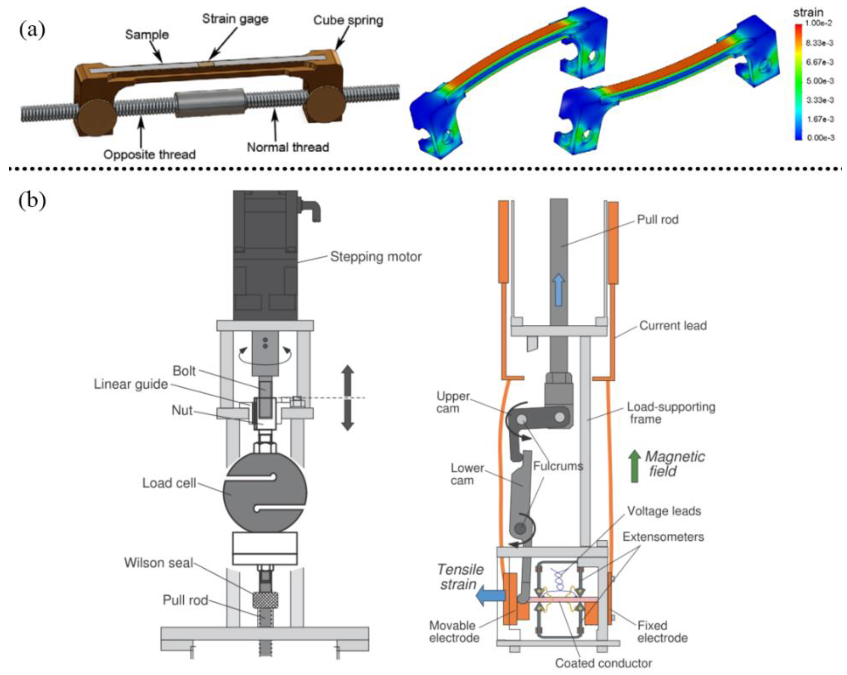
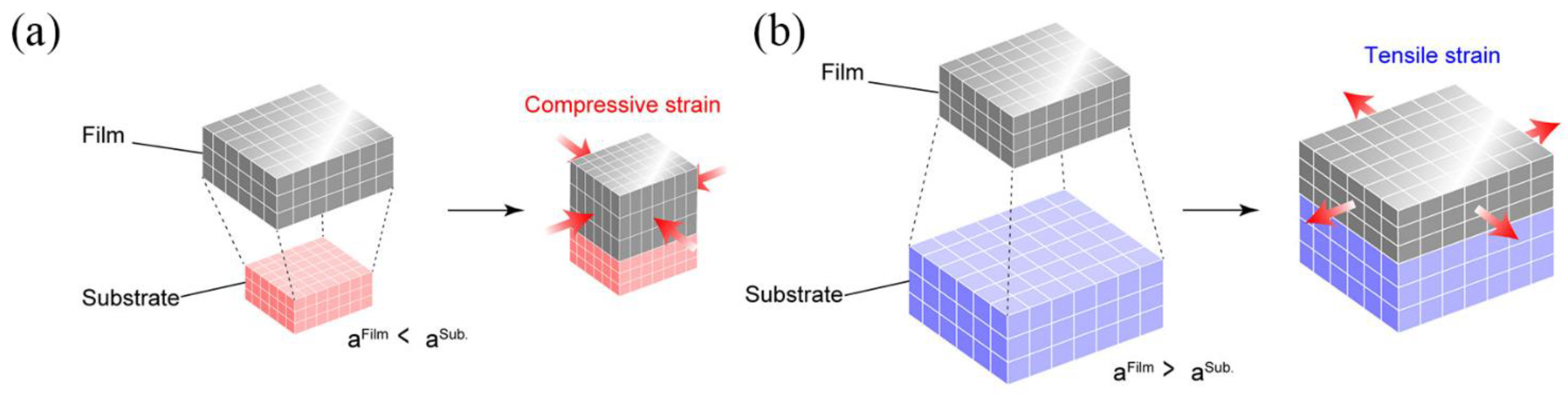
2. Strain Application Methods
3. Strain Measurement Techniques
3.1. XRD
3.2. Neutron Diffraction
3.3. Raman Spectroscopy
3.4. EBSD
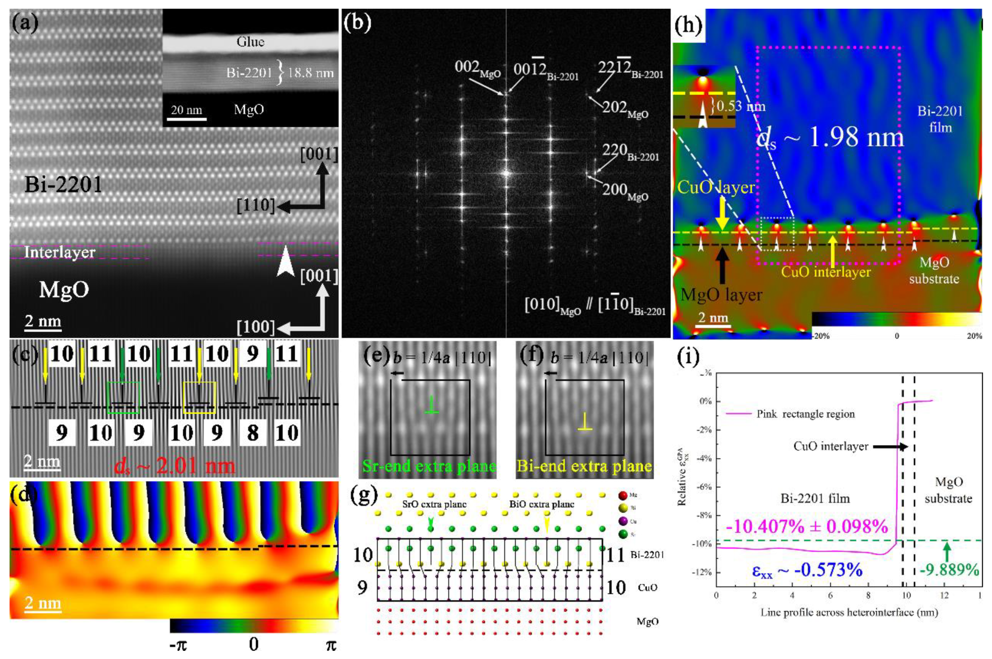
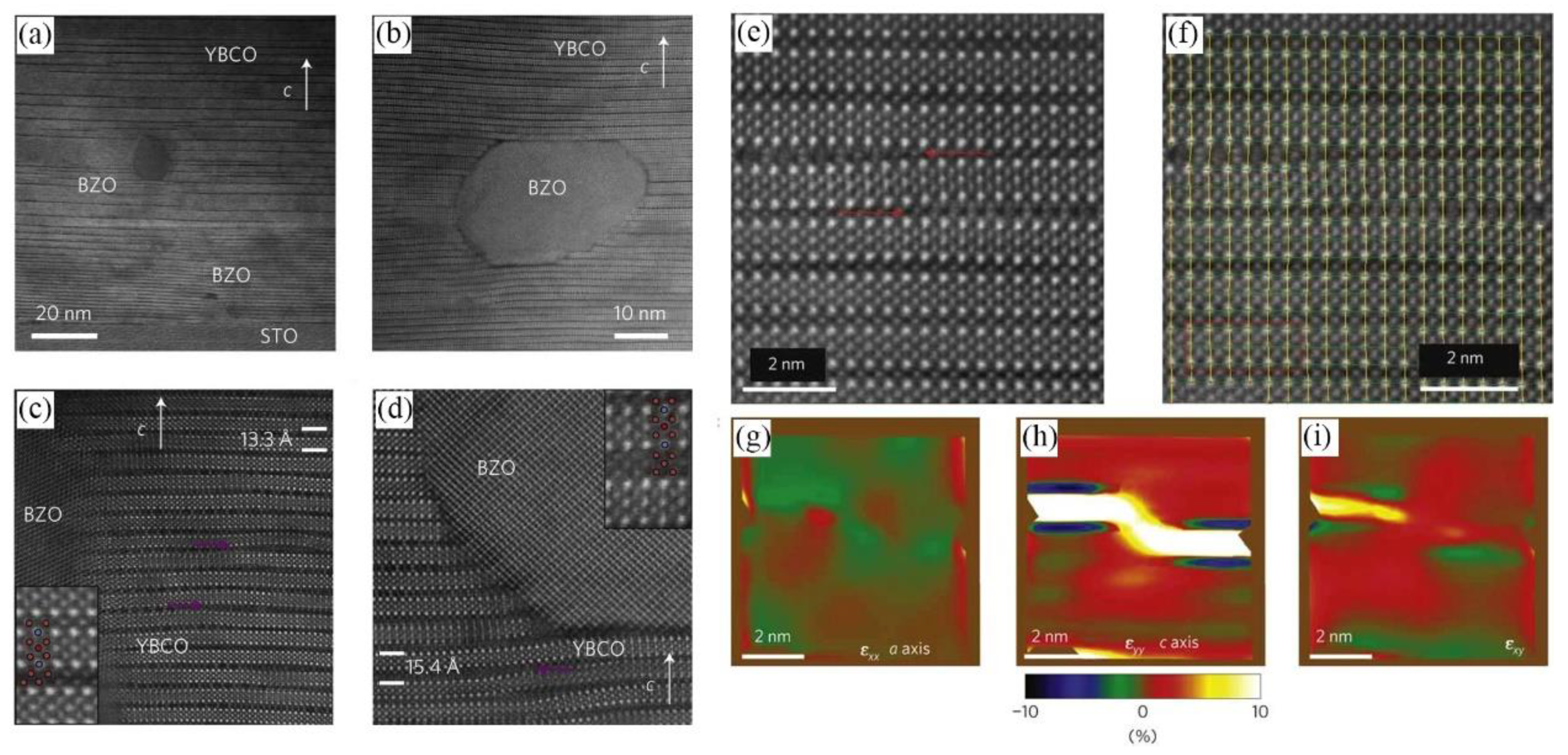
3.5. TEM
4. Effect of Strain on Superconducting Performance
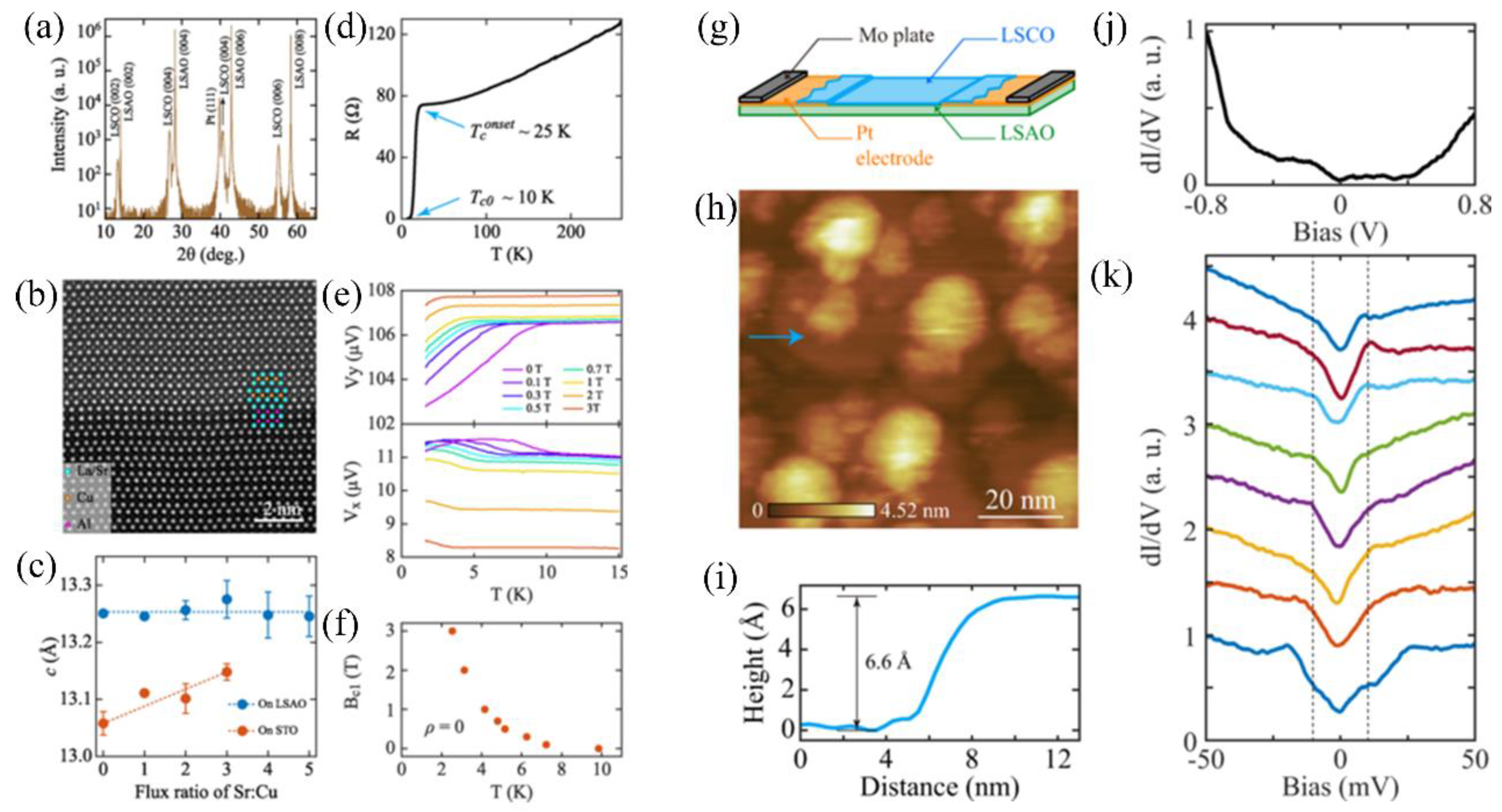
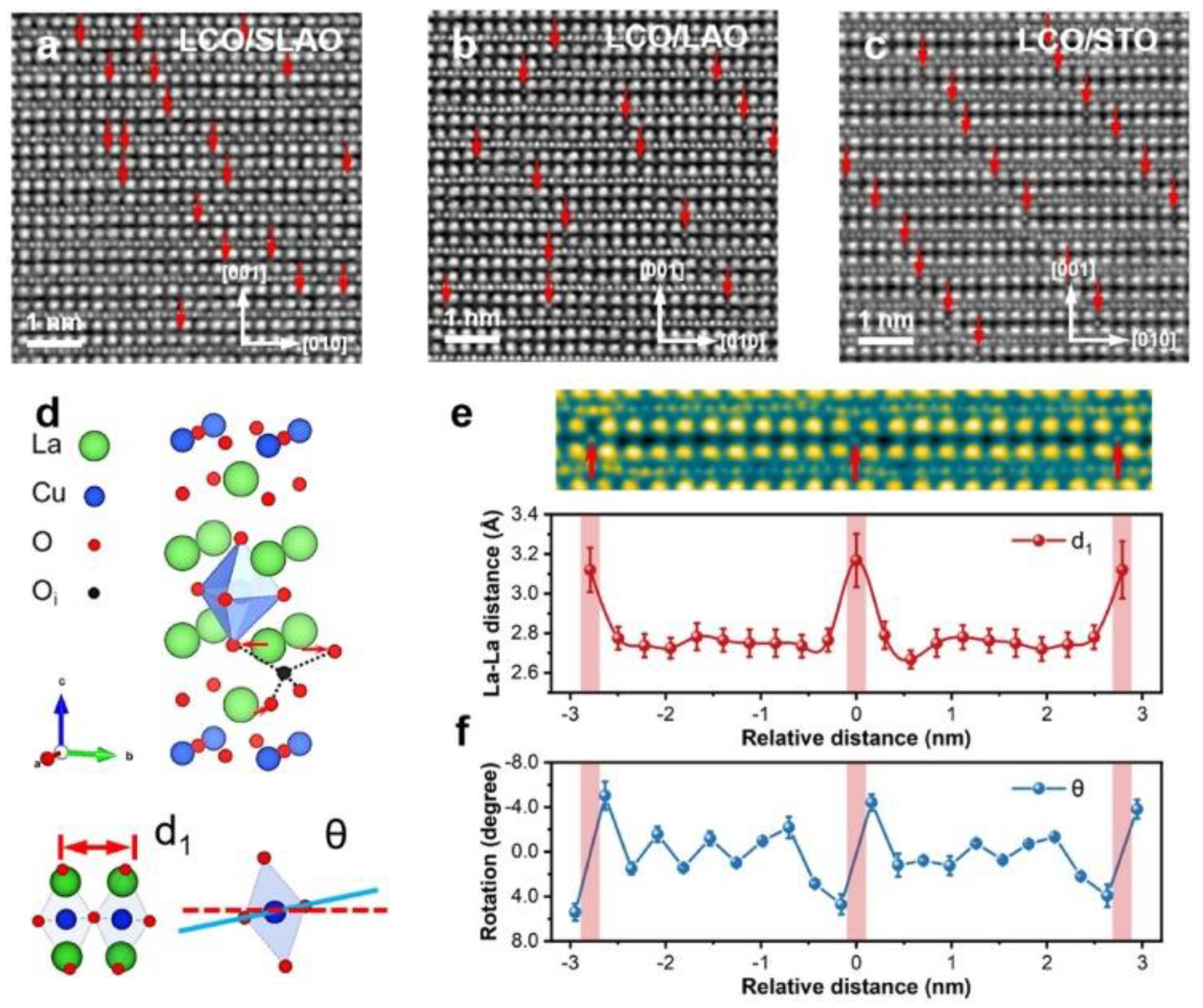
4.1. Effect of Strain on La2−xSrxCuO4+δ System
4.2. Effect of Strain on Bi2Sr2Can−1CunO2n+4+δ System
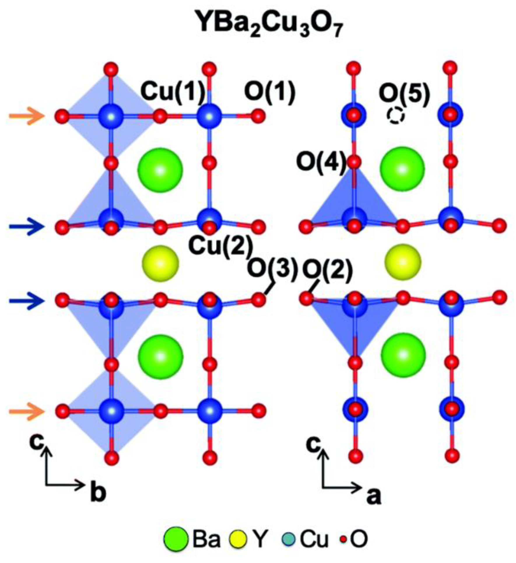
4.3. Effect of Strain on the REBa2Cu3O7−δ System
4.4. Effect of Strain on Other Superconductor Systems
4.5. Effect of Strain on Secondary Phase Vortex Pinning
4.6. Use of Buffer Layers to Release Strain
5. Conclusions and Future Outlook
Author Contributions
Funding
Data Availability Statement
Conflicts of Interest
References
- Wu, M.K.; Ashburn, J.R.; Torng, C.J.; Hor, P.H.; Meng, R.L.; Gao, L.; Huang, Z.J.; Wang, Y.Q.; Chu, C.W. Superconductivity at 93 K in a new mixed-phase Y-Ba-Cu-O compound system at ambient pressure. Phys. Rev. Lett. 1987, 58, 908–910. [Google Scholar] [CrossRef] [PubMed]
- Schilling, A.; Cantoni, M.; Guo, J.D.; Ott, H.R. Superconductivity above 130 K in the Hg-Ba-Ca-Cu-O system. Nature 1993, 363, 56–58. [Google Scholar] [CrossRef]
- Parkin, S.S.P.; Lee, V.Y.; Engler, E.M.; Nazzal, A.I.; Huang, T.C.; Gorman, G.; Savoy, R.; Beyers, R. Bulk superconductivity at 125 K in Tl2Ca2Ba2Cu3Ox. Phys. Rev. Lett. 1988, 60, 2539–2542. [Google Scholar] [CrossRef] [PubMed]
- Maeda, H.; Tanaka, Y.; Fukutomi, M.; Asano, T. A New High-Tc Oxide Superconductor without a Rare Earth Element. Jpn. J. Appl. Phys. 1988, 27, L209–L210. [Google Scholar] [CrossRef]
- Klein, N. High-frequency applications of high-temperature superconductor thin films. Rep. Prog. Phys. 2002, 65, 1387–1425. [Google Scholar] [CrossRef]
- Simsek, Y.; Vlasko-Vlasov, V.; Koshelev, A.E.; Benseman, T.; Hao, Y.; Kesgin, I.; Claus, H.; Pearson, J.; Kwok, W.K.; Welp, U. Thick Bi2Sr2CaCu2O8+δ films grown by liquid-phase epitaxy for Josephson THz applications. Supercond. Sci. Technol. 2018, 31, 015009. [Google Scholar] [CrossRef]
- Koch, R.H.; Umbach, C.P.; Clark, G.J.; Chaudhari, P.; Laibowitz, R.B. Quantum interference devices made from superconducting oxide thin films. Appl. Phys. Lett. 1987, 51, 200–202. [Google Scholar] [CrossRef]
- Zeljkovic, I.; Nieminen, J.; Huang, D.; Chang, T.R.; He, Y.; Jeng, H.T.; Xu, Z.; Wen, J.; Gu, G.; Lin, H.; et al. Nanoscale interplay of strain and doping in a high-temperature superconductor. Nano Lett. 2014, 14, 6749–6753. [Google Scholar] [CrossRef]
- Foltyn, S.R.; Wang, H.; Civale, L.; Maiorov, B.; Jia, Q.X. The role of interfacial defects in enhancing the critical current density of YBa2Cu3O7−δ coatings. Supercond. Sci. Technol. 2009, 22, 125002–125005. [Google Scholar] [CrossRef]
- Locquet, J.-P.; Perret, J.; Fompeyrine, J.; Mächler, E.; Seo, J.W.; Tendeloo, G.V. Doubling the critical temperature of La1.9Sr0.1CuO4 using epitaxial strain. Nature 1998, 194, 453–456. [Google Scholar] [CrossRef]
- Bagués, N.; Santiso, J.; Esser, B.D.; Williams, R.E.A.; McComb, D.W.; Konstantinovic, Z.; Balcells, L.; Sandiumenge, F. The misfit dislocation core phase in complex oxide heteroepitaxy. Adv. Funct. Mater. 2018, 28, 1704437. [Google Scholar] [CrossRef]
- Arredondo, M.; Ramasse, Q.M.; Weyland, M.; Mahjoub, R.; Vrejoiu, I.; Hesse, D.; Browning, N.D.; Alexe, M.; Munroe, P.; Nagarajan, V. Direct Evidence for Cation Non-Stoichiometry and Cottrell Atmospheres Around Dislocation Cores in Functional Oxide Interfaces. Adv. Mater. 2010, 22, 2430–2434. [Google Scholar] [CrossRef] [PubMed]
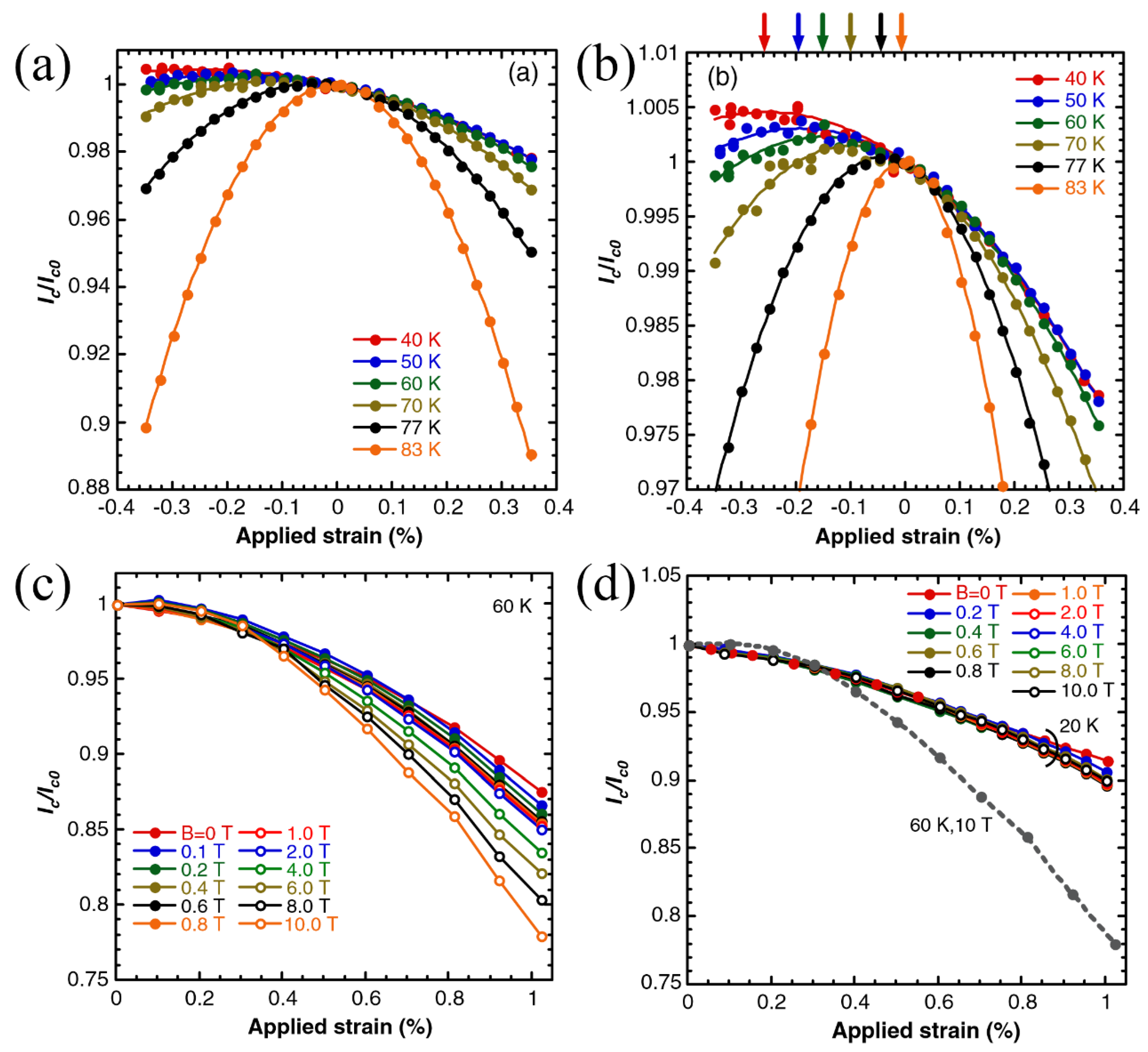
- Sugano, M.; Shikimachi, K.; Hirano, N.; Nagaya, S. The reversible strain effect on critical current over a wide range of temperatures and magnetic fields for YBCO coated conductors. Supercond. Sci. Technol. 2010, 23, 085013. [Google Scholar] [CrossRef]
- Sugano, M.; Nakamura, T.; Manabe, T.; Shikimachi, K.; Hirano, N.; Nagaya, S. The intrinsic strain effect on critical current under a magnetic field parallel to the c axis for a MOCVD-YBCO-coated conductor. Supercond. Sci. Technol. 2008, 21, 115019. [Google Scholar] [CrossRef]
- Cheggour, N.; Ekin, J.W.; Clickner, C.C.; Verebelyi, D.T.; Thieme, C.L.H.; Feenstra, R.; Goyal, A. Reversible axial-strain effect and extended strain limits in Y-Ba-Cu-O coatings on deformation-textured substrates. Appl. Phys. Lett. 2003, 83, 4223–4225. [Google Scholar] [CrossRef]
- Pavarini, E.; Dasgupta, I.; Saha-Dasgupta, T.; Jepsen, O.; KAndersen, O. Band-structure trend in hole-doped cuprates and correlation with Tc max. Phys. Rev. Lett. 2001, 87, 047003. [Google Scholar] [CrossRef]
- Bergman, D.L.; Pereg-Barnea, T. The origin of Tc enhancement in heterostructure cuprate superconductors. Materials 2011, 4, 1835–1845. [Google Scholar] [CrossRef]
- Ohta, Y.; Tohyama, T.; Maekawa, S. Apex oxygen and critical temperature in copper oxide superconductors: Universal correlation with the stability of local singlets. Phys. Rev. B Condens. Matter 1991, 43, 2968–2982. [Google Scholar] [CrossRef]
- Mori, M.; Khaliullin, G.; Tohyama, T.; Maekawa, S. Origin of spatial variation of pairing gap in Bi-based high-Tc cuprates. Phys. Rev. Lett. 2008, 101, 3382–3390. [Google Scholar] [CrossRef]
- Locquet, J.-Ρ.; Williams, L.J. Epitaxially induced defects in Sr- and O-doped La2CuO4 thin films grown by MBE: Implications for transport properties. Acta Phys. Pol. A 1997, 92, 69–84. [Google Scholar] [CrossRef]
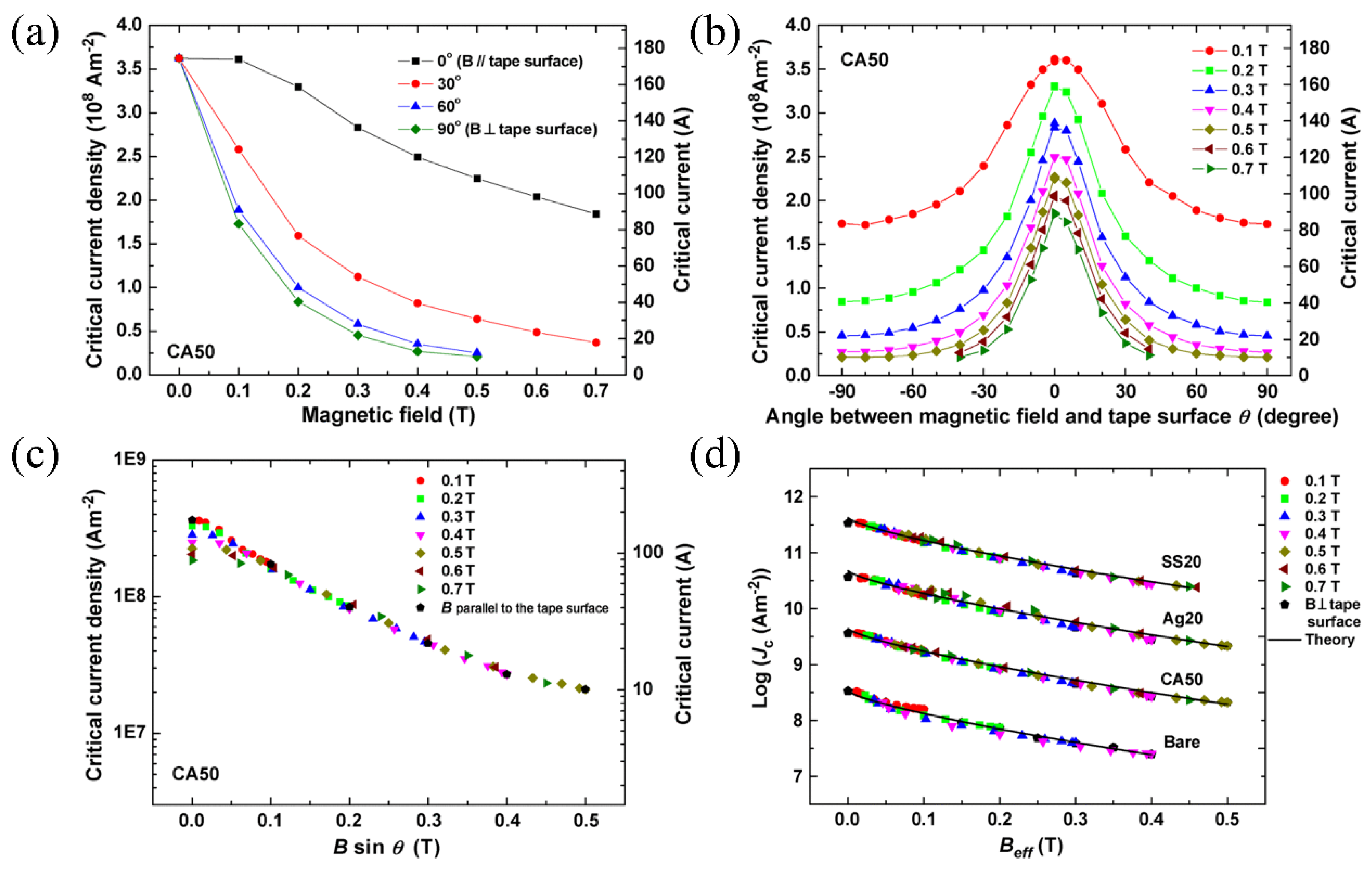
- van der Laan, D.C.; Ekin, J.W.; Douglas, J.F.; Clickner, C.C.; Stauffer, T.C.; Goodrich, L.F. Effect of strain, magnetic field and field angle on the critical current density of YBa2Cu3O7−δ coated conductors. Supercond. Sci. Technol. 2010, 23, 072001. [Google Scholar] [CrossRef]
- Sato, H.; Hiramatsu, H.; Kamiya, T.; Hosono, H. Strain Engineering at Heterointerfaces: Application to an Iron Pnictide Superconductor, Cobalt-Doped BaFe2As2. ACS Appl. Mater. Inter. 2020, 12, 50096–50104. [Google Scholar] [CrossRef] [PubMed]
- Yu, J.; Li, F.; Fan, J.; Muhammad, S.; Dahal, Y.P.; Zhang, Z.; Wang, S. Macroscopic residual stress and properties in different YBa2Cu3O7-x heterogeneous systems. Phys. C Supercond. Its Appl. 2020, 577, 1353728. [Google Scholar] [CrossRef]
- Li, Z.; Coll, M.; Mundet, B.; Palau, A.; Puig, T.; Obradors, X. Suppression of superconductivity at the nanoscale in chemical solution derived YBa2Cu3O7−δ thin films with defective Y2Ba4Cu8O16 intergrowths. Nanoscale Adv. 2020, 2, 3384–3393. [Google Scholar] [CrossRef]
- Osamura, K.; Machiya, S.; Tsuchiya, Y.; Suzuki, H. Force free strain exerted on a YBCO layer at 77 K in surround Cu stabilized YBCO coated conductors. Supercond. Sci. Technol. 2010, 23, 045020. [Google Scholar] [CrossRef]
- Favre, S.; Ariosa, D.; Yelpo, C.; Mazini, M.; Faccio, R. Depression of critical temperature due to residual strain induced by PLD deposition on YBa2Cu3O7-δ thin films. Mater. Chem. Phys. 2021, 266, 124507. [Google Scholar] [CrossRef]
- Koblischka-Veneva, A.; Koblischka, M.R. Residual Stress/Strain Analysis of Bulk YBCO Superconductors Using EBSD. IEEE Trans. Appl. Supercond. 2022, 32, 1–5. [Google Scholar] [CrossRef]
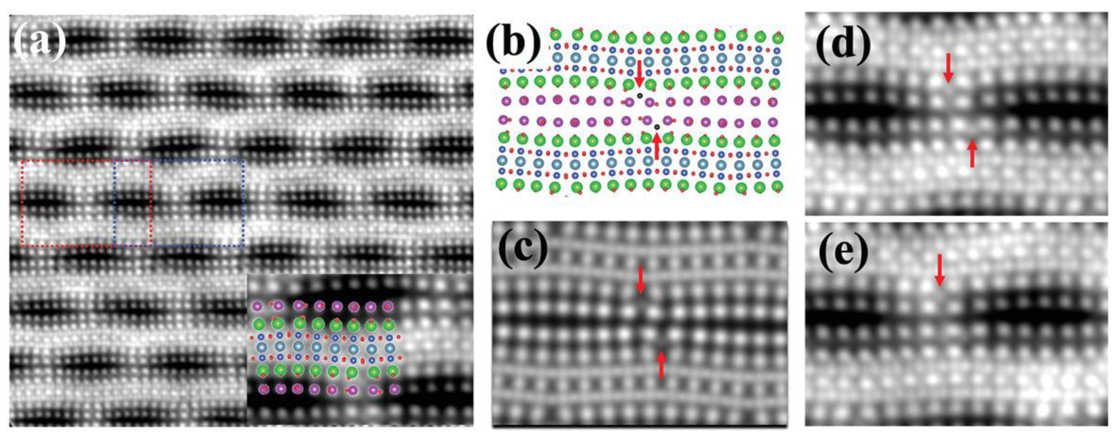
- Zhang, J.; Wang, W.; Wang, T.; Jiang, L.; Wang, N.; Dai, Y.; Wang, M.; Qi, Y. Atomic-scale analysis of the interface structure and lattice mismatch relaxation of Bi2Sr2CaCu2O8+δ/SrTiO3 heterostructure. Ceram. Int. 2021, 47, 8722–8727. [Google Scholar] [CrossRef]
- Zhang, J.; Wang, W.; Wang, N.; Wang, M.; Qi, Y. Atomic-resolution study on the interface structure and strain state reversion of the Bi2Sr2CuO6+δ/MgO heterostructure. J. Colloid Interf. Sci. 2021, 592, 291–295. [Google Scholar] [CrossRef]
- Wang, Y.; Liu, X.P.; Qin, G.W. Strain analysis of misfit dislocations in α-Fe2O3/α-Al2O3 heterostructure interface by geometric phase analysis. Micron 2015, 69, 21–24. [Google Scholar] [CrossRef]
- Hÿtch, M.J.; Snoeck, E.; Kilaas, R. Quantitative measurement of displacement and strain fields from HREM micrographs. Ultramicroscopy 1998, 74, 131–146. [Google Scholar] [CrossRef]
- Bierwolf, R.; Hohenstein, M.; Phillipp, F.; Brandt, O.; Crook, G.E.; Ploog, K. Direct measurement of local lattice distortions in strained layer structures by HREM. Ultramicroscopy 1993, 49, 273–285. [Google Scholar] [CrossRef]
- Zhu, Y.; Ophus, C.; Ciston, J.; Wang, H. Interface lattice displacement measurement to 1 pm by geometric phase analysis on aberration-corrected HAADF STEM images. Acta Materialia 2013, 61, 5646–5663. [Google Scholar] [CrossRef]
- Uesugi, F.; Hokazono, A.; Takeno, S. Evaluation of two-dimensional strain distribution by STEM/NBD. Ultramicroscopy 2011, 111, 995–998. [Google Scholar] [CrossRef] [PubMed]
- Usuda, K.; Numata, T.; Irisawa, T.; Hirashita, N.; Takagi, S. Strain characterization in SOI and strained-Si on SGOI MOSFET channel using nano-beam electron diffraction (NBD). Mater. Sci. Eng. B 2005, 124–125, 143–147. [Google Scholar] [CrossRef]
- Armigliato, A.; Balboni, R.; Carnevale, G.P.; Pavia, G.; Piccolo, D.; Frabboni, S.; Benedetti, A.; Cullis, A.G. Application of convergent beam electron diffraction to two-dimensional strain mapping in silicon devices. Appl. Phys. Lett. 2003, 82, 2172–2174. [Google Scholar] [CrossRef]
- Hÿtch, M.; Houdellier, F.; Hüe, F.; Snoeck, E. Nanoscale holographic interferometry for strain measurements in electronic devices. Nature 2008, 453, 1086–1089. [Google Scholar] [CrossRef] [PubMed]
- Hÿtch, M.J.; Minor, A.M. Observing and measuring strain in nanostructures and devices with transmission electron microscopy. MRS Bull. 2014, 39, 138–146. [Google Scholar] [CrossRef]
- Cooper, D.; Denneulin, T.; Bernier, N.; Beche, A.; Rouviere, J.L. Strain mapping of semiconductor specimens with nm-scale resolution in a transmission electron microscope. Micron 2016, 80, 145–165. [Google Scholar] [CrossRef]
- Beche, A.; Rouviere, J.L.; Barnes, J.P.; Cooper, D. Strain measurement at the nanoscale: Comparison between convergent beam electron diffraction, nano-beam electron diffraction, high resolution imaging and dark field electron holography. Ultramicroscopy 2013, 131, 10–23. [Google Scholar] [CrossRef]
- Okada, H.; Takahashi, H.; Matsuishi, S.; Hirano, M.; Hosono, H.; Matsubayashi, K.; Uwatoko, Y.; Takahashi, H. Pressure dependence of the superconductor transition temperature of Ca(Fe1-xCox)AsF compounds: A comparison with the effect of pressure on LaFeAsO1-xFx. Phys. Rev. B 2010, 81, 054507. [Google Scholar] [CrossRef]
- Chen, X.J.; Struzhkin, V.V.; Yu, Y.; Goncharov, A.F.; Lin, C.T.; Mao, H.K.; Hemley, R.J. Enhancement of superconductivity by pressure-driven competition in electronic order. Nature 2010, 466, 950–953. [Google Scholar] [CrossRef] [PubMed]
- Takahashi, H.; Igawa, K.; Arii, K.; Kamihara, Y.; Hirano, M.; Hosono, H. Superconductivity at 43 K in an iron-based layered compound LaO1-xFxFeAs. Nature 2008, 453, 376–378. [Google Scholar] [CrossRef] [PubMed]
- Si, W.; Li, H.-C.; Xi, X. Strain and oxygenation effects on superconductivity of La1.85Sr0.15CuO4 thin films. Appl. Phys. Lett. 1999, 74, 2839–2841. [Google Scholar] [CrossRef]
- Nakamura, F.; Goko, T.; Hori, J.; Uno, Y.; Kikugawa, N.; Fujita, T. Role of two-dimensional electronic state in superconductivity in La2-xSrxCuO4. Phys. Rev. B 2000, 61, 107–110. [Google Scholar] [CrossRef]
- Si, W.; Xi, X. Epitaxial-strain-induced insulator-superconductor transition in undoped and lightly doped La2CuO4. Appl. Phys. Lett. 2001, 78, 240–242. [Google Scholar] [CrossRef]
- Zeng, X.; Si, W.; Stum, Z.; Xi, X. Doping dependence of superconducting properties in pulsed-laser-deposited La2-xSrxCuO4+δ thin films. IEEE Trans. Appl. Supercond. 2001, 11, 3213–3216. [Google Scholar] [CrossRef]
- Bozovic, I.; Logvenov, G.; Belca, I.; Narimbetov, B.; Sveklo, I. Epitaxial strain and superconductivity in La2-xSrxCuO4 thin films. Phys. Rev. Lett. 2002, 89, 107001. [Google Scholar] [CrossRef]
- Choi, E.M.; Zhu, B.; Lu, P.; Feighan, J.; Sun, X.; Wang, H.; MacManus-Driscoll, J.L. Magnetic signatures of 120 K superconductivity at interfaces in La2CuO4+δ. Nanoscale 2020, 12, 3157–3165. [Google Scholar] [CrossRef]
- Sato, H.; Tsukada, A.; Naito, M.; Matsuda, A. La2-xSrxCuOy epitaxial thin films (x = 0 to 2): Structure, strain, and superconductivity. Phys. Rev. B 2000, 61, 12447–12456. [Google Scholar] [CrossRef]
- Zaytseva, I.; Minikayev, R.; Dobročka, E.; Špankova, M.; Bruyant, N.; Cieplak, M.Z. Structural properties and magnetoresistance of La1.952Sr0.048CuO4 thin films. J. Appl. Phys. 2020, 127, 073901. [Google Scholar] [CrossRef]
- Wang, Y.; Wang, R.-F.; Zhang, Q.; Liao, M.; Gu, L.; Zhang, D.; Song, C.-L.; Ma, X.-C.; Xue, Q.-K. Co-deposition growth and superconductivity of La2−xSrxCuO4 films by reactive molecular beam epitaxy. Phys. Rev. B 2021, 103, 184514. [Google Scholar] [CrossRef]
- Zhang, X.; Zhao, H.; Zhu, J. Visualization and control of oxygen dopant ordering in a cuprate superconductor. Mater. Today Phys. 2022, 23, 100629. [Google Scholar] [CrossRef]
- Petricek, V.; Gao, Y.; Lee, P.; Coppens, P. X-ray analysis of the incommensurate modulation in the 2:2:1:2 Bi-Sr-Ca-Cu-O superconductor including the oxygen atoms. Phys. Rev. B 1990, 42, 387–392. [Google Scholar] [CrossRef]
- Le, P.Y.; Mckinnon, W.R.; Tarascon, J.; Barboux, P. Origin of the incommensurate modulation of the 80-K superconductor Bi2Sr2CaCu2O8.21 derived from isostructural commensurate Bi10Sr15Fe10O46. Phys. Rev. B 1989, 40, 6810–6816. [Google Scholar] [CrossRef]
- Subramanian, M.A.; Torardi, C.C.; Calabrese, J.C.; Gopalakrishnan, J.; Morrissey, K.J.; Askew, T.R.; Flippen, R.B.; Chowdhry, U.; Sleight, A.W. A New High-Temperature Superconductor: Bi2Sr3-xCaxCu2O8+y. Science 1988, 239, 1015–1017. [Google Scholar] [CrossRef]
- Zeljkovic, I.; Main, E.J.; Williams, T.L.; Boyer, M.C.; Chatterjee, K.; Wise, W.D.; Yin, Y.; Zech, M.; Pivonka, A.; Kondo, T.; et al. Scanning tunnelling microscopy imaging of symmetry-breaking structural distortion in the bismuth-based cuprate superconductors. Nat. Mater. 2012, 11, 585–589. [Google Scholar] [CrossRef]
- Haken, B.t.; Kate, H.H.J.t.; Tenbrink, J. Compressive and tensile axial strain reduced critical currents in Bi-2212 conductors. IEEE Trans. Appl. Supercond. 1995, 5, 1298–1301. [Google Scholar] [CrossRef]
- Sunwong, P.; Higgins, J.S.; Hampshire, D.P. Angular, Temperature, and Strain Dependencies of the Critical Current of DI-BSCCO Tapes in High Magnetic Fields. IEEE Trans. Appl. Supercond. 2011, 21, 2840–2844. [Google Scholar] [CrossRef]
- Forro, L.; Ilakovac, V.V.; Keszei, B. High-pressure study of Bi2Sr2CaCu2O8 single crystals. Phys. Rev. B Condens. Matter. 1990, 41, 9551–9554. [Google Scholar] [CrossRef]
- Klotz, S.; Schilling, J.S. Hydrostatic pressure dependence of the superconducting transition temperature to 7 GPa in Bi2Ca1Sr2Cu2O8+y as a function of oxygen content. Phys. C Supercond. 1993, 209, 499–506. [Google Scholar] [CrossRef]
- Chen, X.-J.; Struzhkin, V.V.; Hemley, R.J.; Mao, H.-K.; Kendziora, C. High-pressure phase diagram of Bi2Sr2CaCu2O8+δ single crystals. Phys. Rev. B 2004, 70, 214502. [Google Scholar] [CrossRef]
- Song, D.; Zhang, X.; Lian, C.; Liu, H.; Alexandrou, I.; LaziĆ, I.; G, E.; Bosch, T.; Zhang, D.; Wang, L.; et al. Visualization of Dopant Oxygen Atoms in a Bi2Sr2CaCu2O8+δ Superconductor. Adv. Funct. Mater. 2019, 1603843–1603848. [Google Scholar] [CrossRef]
- Mundet, B.; Hartman, S.T.; Guzman, R.; Idrobo, J.C.; Obradors, X.; Puig, T.; Mishra, R.; Gazquez, J. Local strain-driven migration of oxygen vacancies to apical sites in YBa2Cu3O7-x. Nanoscale 2020, 12, 5922–5931. [Google Scholar] [CrossRef]
- Laan, D.C.v.d.; Ekin, J.W. Large intrinsic effect of axial strain on the critical current of high-temperature superconductors for electric power applications. Appl. Phys. Lett. 2007, 90, 052506. [Google Scholar] [CrossRef]
- Barth, C.; Weiss, K.P.; Goldacker, W. Influence of shear stress on current carrying capabilities of high temperature superconductor tapes. IEEE Trans. Appl. Supercond. 2011, 21, 3098–3101. [Google Scholar] [CrossRef]
- van der Laan, D.C.; Haugan, T.J.; Barnes, P.N. Effect of a compressive uniaxial strain on the critical current density of grain boundaries in superconducting YBa2Cu3O7-δ films. Phys. Rev. Lett. 2009, 103, 027005. [Google Scholar] [CrossRef]
- Guzman, R.; Gazquez, J.; Mundet, B.; Coll, M.; Obradors, X.; Puig, T. Probing localized strain in solution-derived YBa2Cu3O7−δ nanocomposite thin films. Phys. Rev. Mater. 2017, 1, 024801. [Google Scholar] [CrossRef]
- Yugay, K.N.; Muravjev, A.V.; Seropyan, G.M.; Konovalenko, K.B.; Huh, Y. Thin films of high-Tc YBCO with frozen strains. Low Temp. Phys. 2006, 32, 55–60. [Google Scholar] [CrossRef]
- Obradors, X.; Martínez-Julián, F.; Zalamova, K.; Vlad, V.R.; Pomar, A.; Palau, A.; Llordés, A.; Chen, H.; Coll, M.; Ricart, S.; et al. Nucleation and mesostrain influence on percolating critical currents of solution derived YBa2Cu3O7 superconducting thin films. Phys. C Supercond. Its Appl. 2012, 482, 58–67. [Google Scholar] [CrossRef]
- Pahlke, P.; Trommler, S.; Holzapfel, B.; Schultz, L.; Hühne, R. Dynamic variation of biaxial strain in optimally doped and underdoped YBa2Cu3O7−δ thin films. J. Appl. Phys. 2013, 113, 123907. [Google Scholar] [CrossRef]
- Putzky, D.; Radhakrishnan, P.; Wang, Y.; Wochner, P.; Christiani, G.; Minola, M.; van Aken, P.A.; Logvenov, G.; Benckiser, E.; Keimer, B. Strain-induced structural transition in DyBa2Cu3O7−x films grown by atomic layer-by-layer molecular beam epitaxy. Appl. Phys. Lett. 2020, 117, 072601. [Google Scholar] [CrossRef]
- Tan, S.; Zhang, Y.; Xia, M.; Ye, Z.; Chen, F.; Xie, X.; Peng, R.; Xu, D.; Fan, Q.; Xu, H. Interface-induced superconductivity and strain-dependent spin density waves in FeSe/SrTiO3 thin films. Nat. Mater. 2013, 12, 634–640. [Google Scholar] [CrossRef] [PubMed]
- He, S.; He, J.; Zhang, W.; Zhao, L.; Liu, D.; Liu, X.; Mou, D.; Ou, Y.-B.; Wang, Q.-Y.; Li, Z. Phase diagram and electronic indication of high-temperature superconductivity at 65 K in single-layer FeSe films. Nat. Mater. 2013, 12, 605–610. [Google Scholar] [CrossRef]
- Ge, J.-F.; Liu, Z.-L.; Liu, C.; Gao, C.-L.; Qian, D.; Xue, Q.-K.; Liu, Y.; Jia, J.-F. Superconductivity above 100 K in single-layer FeSe films on doped SrTiO3. Nat. Mater. 2015, 14, 285–289. [Google Scholar] [CrossRef]
- Zhang, S.J.; Wang, X.C.; Sammynaiken, R.; Tse, J.S.; Yang, L.X.; Li, Z.; Liu, Q.Q.; Desgreniers, S.; Yao, Y.; Liu, H.Z.; et al. Effect of pressure on the iron arsenide superconductor LixFeAs (x = 0.8, 1.0, 1.1). Phys. Rev. B 2009, 80, 014056. [Google Scholar] [CrossRef]
- Ekin, J.W. Effect of transverse compressive stress on the critical current and upper critical field of Nb3Sn. J. Appl. Phys. 1987, 62, 4829–4834. [Google Scholar] [CrossRef]
- Ekin, J.W. Strain scaling law for flux pinning in practical superconductors. Part 1: Basic relationship and application to Nb3Sn conductors. Cryogenics 1980, 20, 611–624. [Google Scholar] [CrossRef]
- Keys, S.A.; Koizumi, N.; Hampshire, D.P. The strain and temperature scaling law for the critical current density of a jelly-roll Nb3Al strand in high magnetic fields. Supercond. Sci. Technol. 2002, 15, 991–1010. [Google Scholar] [CrossRef]
- Markiewicz, W.D. Comparison of strain scaling functions for the strain dependence of composite Nb3Sn superconductors. Supercond. Sci. Technol. 2008, 21, 054004. [Google Scholar] [CrossRef]
- Lu, X.F.; Taylor, D.M.J.; Hampshire, D.P. Critical current scaling laws for advanced Nb3Sn superconducting strands for fusion applications with six free parameters. Supercond. Sci. Technol. 2008, 21, 105016. [Google Scholar] [CrossRef]
- Pogrebnyakov, A.V.; Redwing, J.M.; Raghavan, S.; Vaithyanathan, V.; Schlom, D.G.; Xu, S.Y.; Li, Q.; Tenne, D.A.; Soukiassian, A.; Xi, X.X.; et al. Enhancement of the Superconducting Transition Temperature of MgB2 by a Strain-Induced Bond-Stretching Mode Softening. Phys. Rev. Lett. 2004, 93, 147006. [Google Scholar] [CrossRef] [PubMed]
- Liu, Y.-C.; Wang, W.-S.; Zhang, F.-C.; Wang, Q.-H. Superconductivity in Sr2RuO4 thin films under biaxial strain. Phys. Rev. B 2018, 97, 224522. [Google Scholar] [CrossRef]
- Ahadi, K.; Galletti, L.; Li, Y.; Salmani-Rezaie, S.; Wu, W.; Stemmer, S. Enhancing superconductivity in SrTiO3 films with strain. Sci. Adv. 2019, 5, eaaw0120. [Google Scholar] [CrossRef] [PubMed]
- Mano, P.; Minamitani, E.; Watanabe, S. Straintronic effect for superconductivity enhancement in Li-intercalated bilayer MoS2. Nanoscale Adv. 2020, 2, 3150–3155. [Google Scholar] [CrossRef]
- Llordés, A.; Palau, A.; Gázquez, J.; Coll, M.; Vlad, R.; Pomar, A.; Arbiol, J.; Guzmán, R.; Ye, S.; Rouco, V.; et al. Nanoscale strain-induced pair suppression as a vortex-pinning mechanism in high-temperature superconductors. Nat. Mater. 2012, 11, 329–336. [Google Scholar] [CrossRef]
- Li, Z.; Coll, M.; Mundet, B.; Chamorro, N.; Valles, F.; Palau, A.; Gazquez, J.; Ricart, S.; Puig, T.; Obradors, X. Control of nanostructure and pinning properties in solution deposited YBa2Cu3O7-x nanocomposites with preformed perovskite nanoparticles. Sci. Rep. 2019, 9, 5828. [Google Scholar] [CrossRef]
- Cayado, P.; Mundet, B.; Eloussifi, H.; Vallés, F.; Coll, M.; Ricart, S.; Gázquez, J.; Palau, A.; Roura, P.; Farjas, J.; et al. Epitaxial superconducting GdBa2Cu3O7−δ/Gd2O3 nanocomposite thin films from advanced low-fluorine solutions. Supercond. Sci. Technol. 2017, 30, 125010. [Google Scholar] [CrossRef]
- Solano, E.; Geenen, F.; Puig, T.; Obradors, X.; Mocuta, C.; Detavernier, C. Axiotaxy in oxide heterostructures: Preferential orientation of BaCeO3 nanoparticles embedded in superconducting YBa2Cu3O7−δ thin films. Thin Solid Films 2017, 638, 105–113. [Google Scholar] [CrossRef]
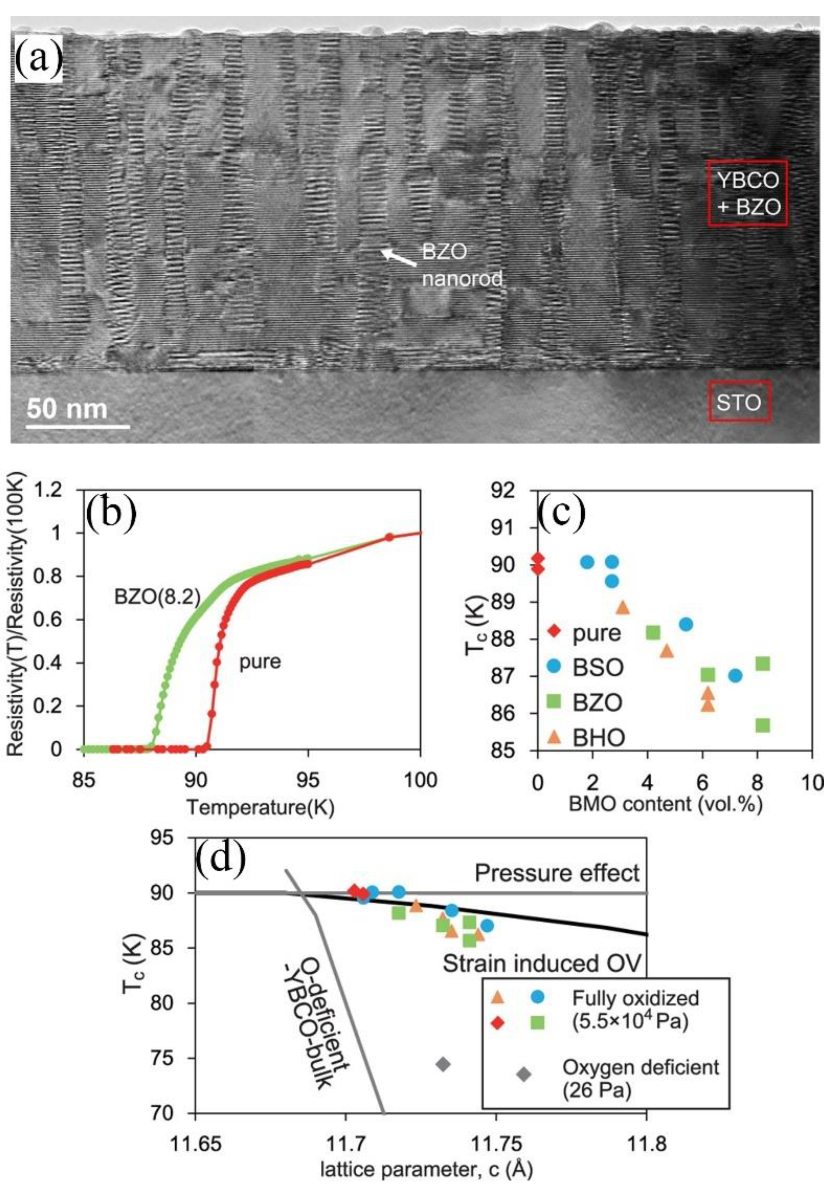
- Cantoni, C.; Gao, Y.; Wee, S.H.; Specht, E.D.; Gazquez, J.; Meng, J.; Pennycook, S.J.; Goyal, A. Strain-driven oxygen deficiency in self-assembled, nanostructured, composite oxide films. ACS Nano 2011, 5, 4783–4789. [Google Scholar] [CrossRef]
- Ye, J.; Mou, S.; Zhu, R.; Liu, L.; Li, Y. Effect and Mechanism of Doping Concentration on Growth and Performance of Thick BaHfO3-doped Y0.5Gd0.5Ba2Cu3O7−δ Films by Pulsed Laser Deposition. J. Supercond. Nov. Magn. 2022, 35, 435–444. [Google Scholar] [CrossRef]
- Miura, S.; Yoshida, Y.; Ichino, Y.; Matsumoto, K.; Ichinose, A.; Awaji, S. Characteristics of high-performance BaHfO3-doped SmBa2Cu3Oy superconducting films fabricated with a seed layer and low-temperature growth. Supercond. Sci. Technol. 2015, 28, 065013. [Google Scholar] [CrossRef]
- Ichino, Y.; Sato, S.; Tsuchiya, Y.; Yoshida, Y. Effect on SmBa2Cu3Oy films of lattice strain induced by BaHfO3 nanorods. Phys. C Supercond. Its Appl. 2020, 575, 1353692. [Google Scholar] [CrossRef]
- Samoilenkov, S.V.; Boytsova, O.V.; Amelichev, V.A.; Kaul, A.R. Anisotropic strain of BaZrO3, BaCeO3 and Y2O3 nanoinclusions in a YBa2Cu3O7 −x epitaxial film matrix and its relation to the oxygen content of the superconductor. Supercond. Sci. Technol. 2011, 24, 055003. [Google Scholar] [CrossRef]
- Horide, T.; Kametani, F.; Yoshioka, S.; Kitamura, T.; Matsumoto, K. Structural evolution induced by interfacial lattice mismatch in self-organized YBa2Cu3O7−δ nanocomposite film. ACS Nano 2017, 11, 1780–1788. [Google Scholar] [CrossRef]
- Gondo, M.; Yoshida, M.; Yoshida, Y.; Ishimaru, M.; Horide, T.; Matsumoto, K.; Kita, R. Nanostructures and flux pinning properties in YBa2Cu3O7−y thin films with double perovskite Ba2LuNbO6 nanorods. J. Appl. Phys. 2021, 129, 195301. [Google Scholar] [CrossRef]
- Mizuno, A.; Tsuchiya, Y.; Awaji, S.; Yoshida, Y. Rectification at various temperatures in YBa2Cu3Oy coated conductors with PrBa2Cu3Oy buffer layers. IEEE Trans. Appl. Supercond. 2022, 32, 1–5. [Google Scholar] [CrossRef]
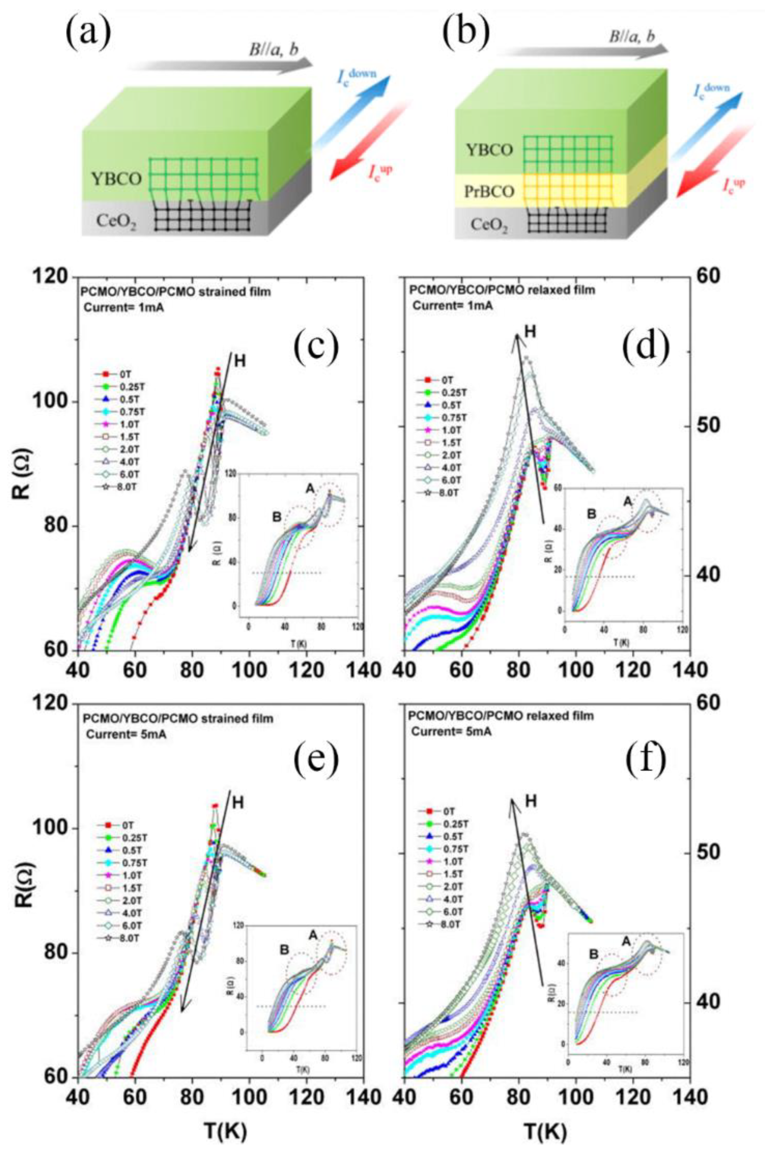
- Kumar Baisnab, D.; Janawadkar, M.P.; Sharma, S.; Sarguna, R.M.; Vaidhyanathan, L.S.; Bharathi, A. The effects of strain, current, and magnetic field on superconductivity in Pr0.5Ca0.5MnO3/YBa2Cu3O7/Pr0.5Ca0.5MnO3 trilayer. J. Appl. Phys. 2013, 113, 113902. [Google Scholar] [CrossRef]
- He, Y.; Ito, M.; Sakuma, K.; Ueda, K.; Asano, H. Preparation and Properties of Sr0.9La0.1CuO2 Thin Films Grown on BaySr1-yTiO3 Layers. IEEE Trans. Appl. Supercond. 2015, 25, 1–4. [Google Scholar] [CrossRef]
- Park, C.; Norton, D.P.; Budai, J.D.; Christen, D.K.; Verebelyi, D.; Feenstra, R.; Lee, D.F.; Goyal, A.; Kroeger, D.M.; Paranthaman, M. Bend strain tolerance of critical currents for YBa2Cu3O7 films deposited on rolled-textured (001)Ni. Appl. Phys. Lett. 1998, 73, 1904–1906. [Google Scholar] [CrossRef]
- Lee, J.; Fujita, K.; McElroy, K.; Slezak, J.A.; Wang, M.; Aiura, Y.; Bando, H.; Ishikado, M.; Masui, T.; Zhu, J.X.; et al. Interplay of electron–lattice interactions and superconductivity in Bi2Sr2CaCu2O8+δ. Nature 2006, 442, 546–550. [Google Scholar] [CrossRef] [PubMed]
- Pan, S.H.; O’Neal, J.P.; Badzey, R.L.; Chamon, C.; Ding, H.; Engelbrecht, J.R.; Wang, Z.; Eisaki, H.; Uchida, S.; Gupta, A.K.; et al. Microscopic electronic inhomogeneity in the high-Tc superconductor Bi2Sr2CaCu2O8+δ. Nature 2001, 413, 282–285. [Google Scholar] [CrossRef] [PubMed]
- Lang, K.M.; Madhavan, V.; Hoffman, J.E.; Hudson, E.W.; Eisaki, H.; Uchida, S.; Davis, J.C. Imaging the granular structure of high-Tc superconductivity in underdoped Bi2Sr2CaCu2O8+δ. Nature 2002, 415, 412–416. [Google Scholar] [CrossRef] [PubMed]
- Gomes, K.K.; Pasupathy, A.N.; Pushp, A.; Ono, S.; Ando, Y.; Yazdani, A. Visualizing pair formation on the atomic scale in the high-Tc superconductor Bi2Sr2CaCu2O8+δ. Nature 2007, 447, 569–572. [Google Scholar] [CrossRef]
- Slezak, J.A.; Lee, J.; Wang, M.; McElroy, K.; Fujita, K.; Andersen, B.M.; Hirschfeld, P.J.; Eisaki, H.; Uchida, S.; Davis, J.C. Imaging the impact on cuprate superconductivity of varying the interatomic distances within individual crystal unit cells. Proc. Natl. Acad. Sci. USA 2008, 105, 3203–3208. [Google Scholar] [CrossRef]
- Zeljkovic, I.; Hoffman, J.E. Interplay of chemical disorder and electronic inhomogeneity in unconventional superconductors. Phys. Chem. Chem. Phys. PCCP 2013, 15, 13462–13478. [Google Scholar] [CrossRef]
- Martin, I.; Balatsky, A.V. Doping-induced inhomogeneity in high-Tc superconductors. Phys. C 2001, 357, 46–48. [Google Scholar] [CrossRef]
- Nunner, T.S.; Andersen, B.M.; Melikyan, A.; Hirschfeld, P.J. Dopant-modulated pair interaction in cuprate superconductors. Phys. Rev. Lett. 2005, 95, 177003. [Google Scholar] [CrossRef]
- Chen, W.; Gabay, M.; Hirschfeld, P.J. Doping dependence of gap inhomogeneities at Bi2Sr2CaCu2O8+δ surfaces. New J. Phys. 2012, 14, 033004. [Google Scholar] [CrossRef]
- Raimondi, R.; Jefferson, J.H.; Feiner, L.F. Effective single-band models for the high-Tc cuprates. II. Role of apical oxygen. Phys. Rev. B 1996, 53, 8774–8788. [Google Scholar] [CrossRef]


| Technique | Precision | Spatial Resolution | Field of View | Advantages | Disadvantages |
|---|---|---|---|---|---|
| HR-(S)TEM | 10−3 | 1 ~ 2 nm | 150 × 150 nm | High availability | Demanding specimen preparation and limited in field of view |
| NBED | 10−3 | 5 ~ 10 nm | — | Practical and versatile | Low spatial resolution |
| CBED | 2 × 10⁻⁴ | 0.5 ~ 2 nm | — | Most accurate technique | Easily interfered by bending atomic columns |
| DFEH | 2 × 10⁻⁴ | 2 ~ 4 nm | 1500 × 500 nm | Largest view areas | Low spatial resolution |
Publisher’s Note: MDPI stays neutral with regard to jurisdictional claims in published maps and institutional affiliations. |
© 2022 by the authors. Licensee MDPI, Basel, Switzerland. This article is an open access article distributed under the terms and conditions of the Creative Commons Attribution (CC BY) license (https://creativecommons.org/licenses/by/4.0/).
Share and Cite
Zhang, J.; Wu, H.; Zhao, G.; Han, L.; Zhang, J. A Review on Strain Study of Cuprate Superconductors. Nanomaterials 2022, 12, 3340. https://doi.org/10.3390/nano12193340
Zhang J, Wu H, Zhao G, Han L, Zhang J. A Review on Strain Study of Cuprate Superconductors. Nanomaterials. 2022; 12(19):3340. https://doi.org/10.3390/nano12193340
Chicago/Turabian StyleZhang, Jian, Haiyan Wu, Guangzhen Zhao, Lu Han, and Jun Zhang. 2022. "A Review on Strain Study of Cuprate Superconductors" Nanomaterials 12, no. 19: 3340. https://doi.org/10.3390/nano12193340