Article

Low-Temperature UVO-Sintered ZnO/SnO2 as Robust Cathode Buffer Layer for Ternary Organic Solar Cells

1
Key Laboratory of Hunan Province on Information Photonics and Freespace Optical Communications, College of Physics and Electronics, Hunan Institute of Science and Technology, Yueyang 414006, China
2
College of Electronic Information and Optical Engineering, Nankai University, Tianjin 300071, China
*
Author to whom correspondence should be addressed.
Nanomaterials 2022, 12(18), 3149; https://doi.org/10.3390/nano12183149
Submission received: 28 July 2022 / Revised: 6 September 2022 / Accepted: 9 September 2022 / Published: 11 September 2022
(This article belongs to the Special Issue First-Principles Investigations of Low-Dimensional Nanomaterials)

Abstract

:
The cathode buffer layer (CBL) plays a crucial role in organic solar cells (OSCs), and it has been challenging to obtain high-quality CBL by using simple and reliable processes. In this paper, the bilayer structure consisting of ZnO nanoparticles (NPs) and sol–gel SnO2 was prepared by the low-temperature (<100 °C) UV-ozone (UVO) sintering process and used as the robust CBL for ternary OSCs based on PTB7-Th:PCDTBT:PC70BM. The results show that the insertion of SnO2 can effectively fill the cracks and pores on the surface of the ZnO NP film, thereby improving the overall compactness and flatness of the CBL and reducing the defect density inside the CBL. Furthermore, the insertion of SnO2 slightly improves the transmittance of the CBL to photons with wavelengths in the range of 400–600 nm, and also increases the electron mobility of the CBL thus facilitating the extraction and transport of the electrons. Compared to the devices using UVO-ZnO and UVO-SnO2 CBLs, the devices with UVO-ZnO/SnO2 CBL exhibit exceptional performance advantages, the best power conversion efficiency (PCE) reaches 10.56%. More importantly, the stability of the devices with ZnO/SnO2 CBL is significantly improved, the device (PCE) still maintains 60% of the initial value after 30 days in air. The positive results show that the UVO-ZnO/SnO2 is an ideal CBL for OSCs, and due to the low-temperature process, it has great application potential in flexible OSCs.

1. Introduction

Solar cells are of great significance in solving the energy shortage crisis and environmental pollution problems faced by mankind. Among various types of solar cells, organic solar cells (OSCs) have become a hot research topic in the field of solar cells due to the advantages of low cost, easy processing, flexible compatibility, and roll-to-roll large area production [1,2,3,4]. In recent years, the power conversion efficiency (PCE) of OSCs has increased substantially, and the laboratory PCE of the single-junction OSCs has now exceeded 19% [5,6]. The steady increase in PCE reveals the research value and application potential of OSCs.
It is well known that the cathode buffer layer (CBL) plays a crucial role in OSCs, and the deposition of the CBL is an important part of the OSCs preparation process, especially in the inverted OSCs, the device performance is largely dependent on the selection of the CBL material [7,8]. The widely used CBL material in inverted OSCs is metal oxide [9,10,11,12], while the zinc oxide (ZnO) nanoparticles (NPs) have become a more favored material by the researchers due to its higher electron mobility and photon transmission as well as lower work function [13,14,15,16]. Unfortunately, further improvement in the PCE of OSCs based on the ZnO NPs is hindered by the presence of defect states. The results of experimental and first-principle calculations have clarified the presence of defects in ZnO NPs [17,18,19]. The calculations based on density-functional theory (DFT) within the general gradient approximation plus Hubbard U indicates that the most favorable defects of the ZnO NPs are Zn and O vacancies [20]; the calculations based on exchange-correlation functionals demonstrates that the oxygen vacancies defect state appears in the valence band of ZnO and acts as a deep donor [21]. Undoubtedly, the photogenerated carriers (holes) annihilate once they meet the electrons released by the deep-level donors, resulting in the reduction of the short-circuit current density (Jsc) and the deterioration of the devices performance. In addition, the ZnO NP films are likely to show surface cracks and pores during the deposition process [22,23,24], resulting in the organic active layer on top of it not being able to form close contact. In short, the higher defect density and poor surface morphology in the ZnO NPs CBL will inevitably increase the probability of the recombination of electrons and holes generated in the active layer [25].
Obviously, reducing the defect density of ZnO NPs CBL and improving the surface morphology quality are effective strategies to improve the PCE of OSCs. The interface engineering therefore has been carried out between the ZnO and active layer by inserting additional layers, such as conjugated polyelectrolytes, fullerene derivative, metal oxides and semiconductor NPs [26,27,28]. Previous studies by our group [29,30] have also shown that insertion layers such as water-soluble conjugated polymer PFN and germanium NPs can effectively reduce the surface defect density of the ZnO NP CBL and strengthen the interfacial contact between the active layer and the ZnO NPs CBL, thereby increasing the Jsc and reducing the series resistance of the devices. Recently, the tin dioxide (SnO2) has appeared to be a better CBL for OSCs due to its high electron mobility, wide bandgap, and low defect density [31,32]. In fact, due to the excellent electrical properties, SnO2 has been widely used as CBLs for perovskite solar cells [33,34,35]. It is foreseeable that using ZnO/SnO2 as the CBL for OSCs, the synergistic effect of the two can effectively promote the PCE of OSCs.
In this paper, we used a facile two-step low-temperature (<100 °C) UV-ozone (UVO) sintering method to fabricate the ZnO/SnO2 bilayer as a robust CBL for the PTB7-Th:PCDTBT:PC70BM ternary OSCs. We observed that the introduction of SnO2 layer can significantly eliminate the cracks and pores on the surface of the ZnO NP film, making the surface morphology denser and smoother, thereby strengthening the interface contact between the CBL and the active layer. In addition, compared with the ZnO monolayer, the ZnO/SnO2 bilayer exhibits higher photon transmittance and electron mobility, which further improves the photon absorption of the active layer while optimizing the electrons transport and extraction. Benefiting from the adoption of the ZnO/SnO2 bilayer CBL, the optimum PCE of the devices was improved by 16.7%, reaching 10.56%. More importantly, the stability of the devices under air atmosphere was significantly enhanced. Our results show that the UVO-ZnO/SnO2 bilayer is an ideal CBL for OSCs, and due to the low-temperature sintering process, the ZnO/SnO2 bilayer has great application potential in flexible OSCs.

2. Experimental Details

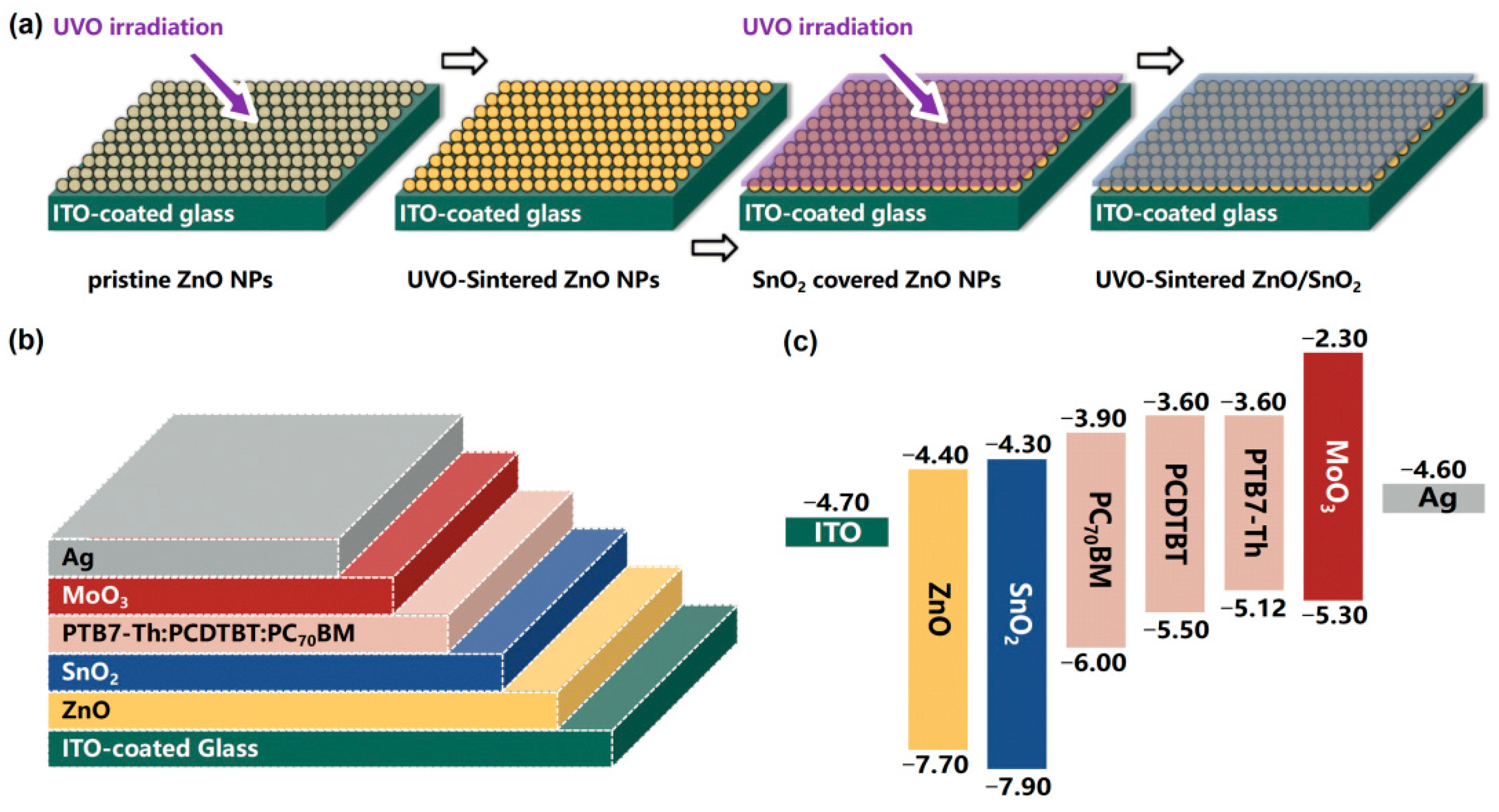
2.1. Fabrication of ZnO/SnO2 Bilayer

The fabrication process of the two-step UVO-ZnO/SnO2 bilayer is shown in Figure 1a. The preparation methods of water-bath ZnO NPs suspension and sol–gel SnO2 can be found in our previous work [35,36]. Generally, the ZnO NPs suspension was synthesized by hydrolysis and condensation of zinc acetate dihydrate by potassium hydroxide in methanol using a Zn2+:OH ratio of 1:1.7, and the sol–gel SnO2 was synthesized by dissolving tin dichloride dihydrate in ethanol to form a solution with a concentration of 0.1 M. The UVO cleaner (YZUV-22C, Beijing Kenuo Instrument Equipment Co., Ltd., Beijing, China) equipped with Hg lamp was used as the platform for irradiating the ZnO monolayer or ZnO/SnO2 bilayer film. The power density of the UV lamp is about 0.5 W/cm2 and the temperature of the substrates during UVO treatment is about 70 °C [29,35]. Firstly, the ZnO NPs was spin-coated on the cleaned commercial indium tin oxide (ITO) coated glass substrate (STN-SI-10, China Southern Glass Group Co., Ltd., Shenzhen, China) and subjected to UVO sintering, then the sol–gel SnO2 precursors was spin-coated on the UVO-ZnO NPs, and UVO sintering was performed again to finally obtain ZnO/SnO2 bilayer film. The sintering time of the ZnO-coated monolayer film and the ZnO/SnO2-coated bilayer film was 20 min and 60 min, respectively.

2.2. Fabrication of OSCs with ZnO/SnO2 CBL

The schematic architecture of the inverted ternary OSCs (ITO/ZnO NPs/SnO2/active layer/MoO3/Ag) are shown in Figure 1b. The mixed PTB7-Th:PCDTBT:PC70BM (0.8:0.2:1.5) was selected as the active layer materials; the mixing ratio optimization process has been described in detail elsewhere [37]. Before device fabrication, the ITO-coated glass substrate was cleaned by ultrasonic treatment in detergent, de-ionized water, acetone and isopropyl alcohol sequentially. Firstly, the ZnO/SnO2 bilayer CBL (about 100-nm thick) was prepared as described above. After, the substrate was transferred into a nitrogen filled glovebox, the blend active layer was deposited by spin-coating (2000 rpm for 30 s) from the pre-prepared PTB7-Th:PCDTBT:PC70BM blend solution, and the preparation method is as follows: the polymers (PTB7-Th and PCDTBT) and PC70BM (1:1.5 w/w) were co-dissolved in the mixed solvent of chlorobenzene and 1,8-diodooctane (97:3 vol/vol). The overall polymer concentration was 10 mg/mL and the solution was stirred at 90 °C for 12 h [37]. The thickness of the active layer is about 100 nm. Finally, a 10-nm thick molybdenum trioxide (MoO3) hole transport layer (HTL) and a 100-nm thick Ag electrode layer were subsequently evaporated through a shadow mask under the pressure of 7.0 × 10⁻⁴ Pa. The devices with the UVO-ZnO NPs CBL (about 50-nm thick) and the UVO-SnO2 CBL (about 50-nm thick) were also fabricated as reference.

2.3. Characterization

The current density–voltage (J–V) measurement of the ternary OSCs were conducted under simulated sunlight of 100 mW/cm2 using AM 1.5G type filter. The external quantum efficiency (EQE) spectra were tested using a Solar Cell Quantum Efficiency Measurement System (QEX10) from PV Measurement, Inc. Scanning electron microscopy (SEM) the atomic force microscopy (AFM) were used to investigate the morphology and roughness, the instrument models are JEOL JSM-7800F and Seiko instrumental SPA 400, respectively. Optical transmittance spectra were measured by spectrophotometer (Cary 5000 UV-VIS). The electron mobility in the electron-only devices was assessed using the space-charge-limited current (SCLC) method [38].

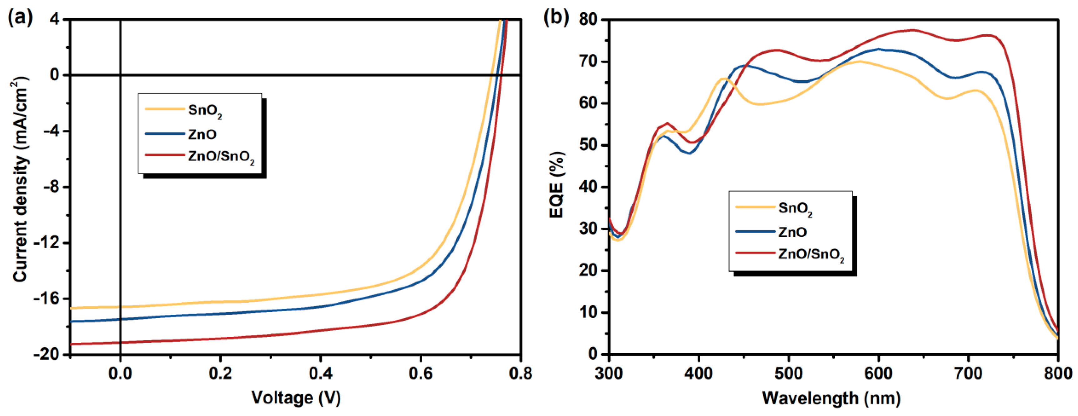
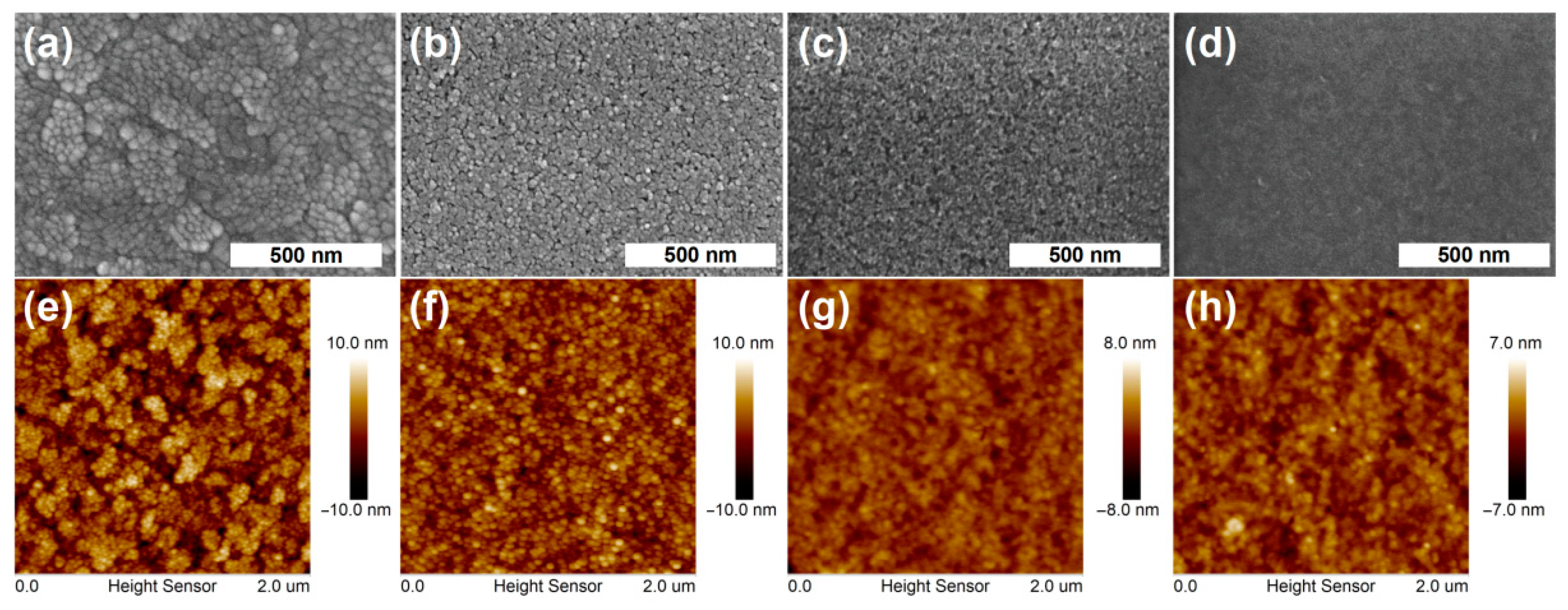
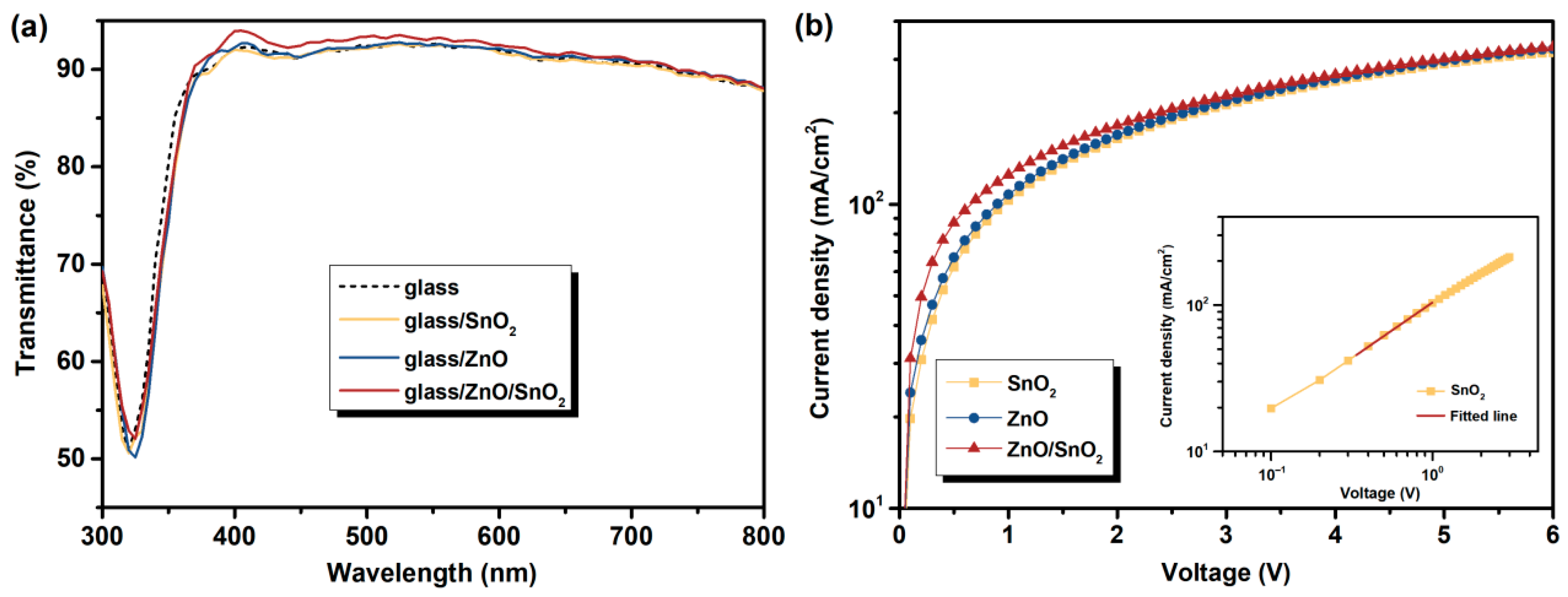
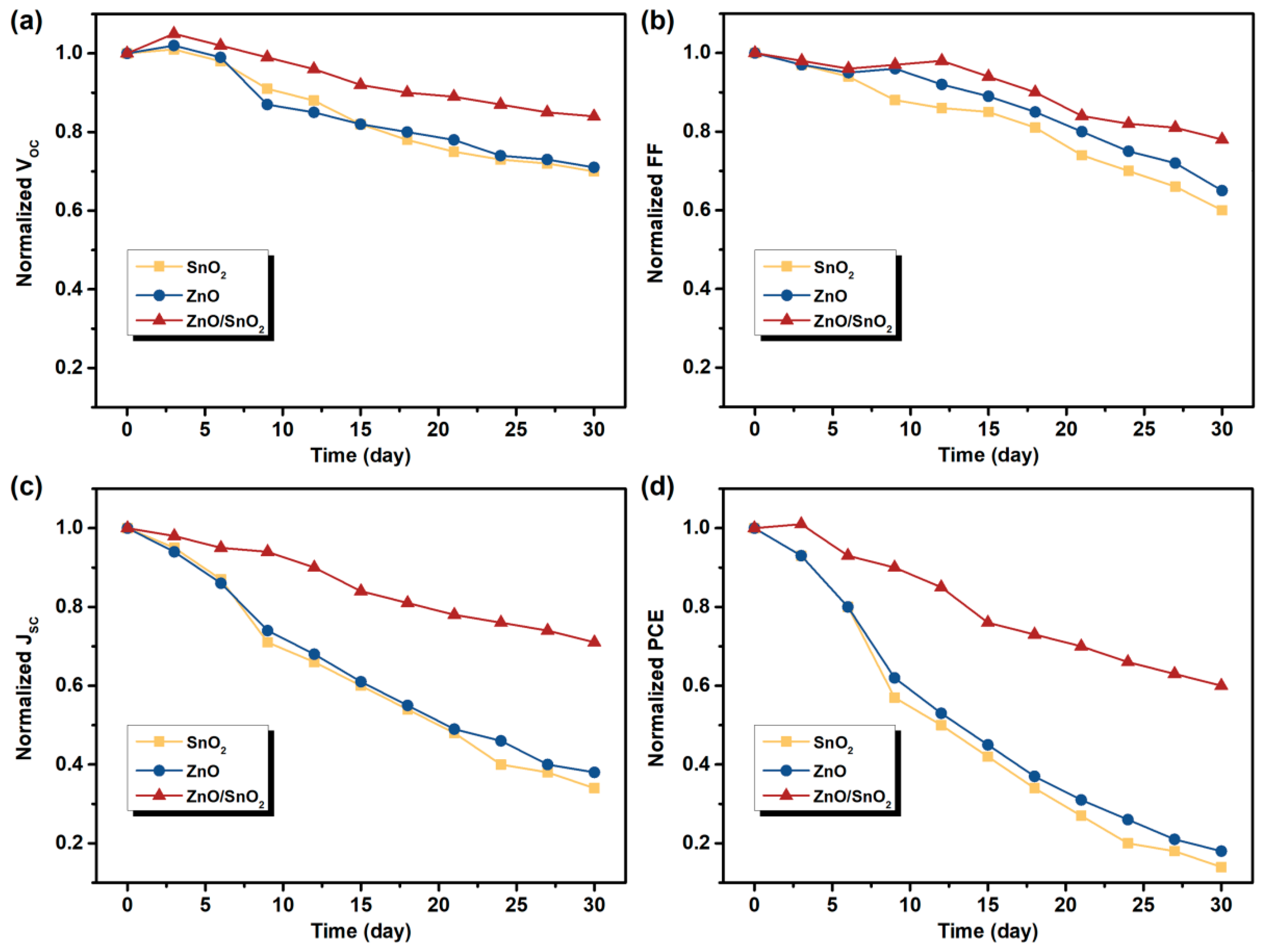
3. Results and Discussion

The energy level of materials are illustrated in Figure 1c. Compared to ZnO, SnO2 exhibits a higher conduction band bottom and a lower valence band top. Apparently, for the ZnO/SnO2 bilayer CBL, the energy cascade of the conduction band bottom is more favorable for the electron extraction and transport [39], while the lower valence band top is more effective in blocking the holes. As a reference, the ternary OSCs based on UVO-ZnO NPs CBL and the UVO-SnO2 CBL were also prepared and fabricated. The current density–voltage (J–V) characteristics of the devices with UVO-ZnO, UVO-SnO2 and UVO-ZnO/SnO2 CBLs are shown in Figure 2a, and the corresponding detailed photovoltaic parameters are summarized in Table 1. The devices based on UVO-ZnO exhibits an optimum PCE of 9.05%, with open circuit voltage (Voc) of 0.761 V, Jsc of 17.72 mA/cm2, and fill factor (FF) of 69.07%. When UVO-SnO2 is employed instead of UVO-ZnO as the CBL, the overall performance of the devices decreases, with a Jsc of 16.33 mA/cm2, an Voc of 0.754 V, an FF of 67.97%, and an optimum PCE of only 8.37%. Compared to the devices using monolayer CBL, the devices with UVO-ZnO/SnO2 bilayer exhibit exceptional performance advantages. The best PCE of the devices reaches 10.56%, which is matched with a Jsc of 19.03 mA/cm2, an Voc of 0.77 V, and an FF of 72.05%.
The positive effects of the UVO-ZnO/SnO2 bilayer CBL on the device performances can also be confirmed from the corresponding external quantum efficiency (EQE) characteristics as shown in Figure 2b. The devices with the UVO-ZnO/SnO2 bilayer CBL exhibits a prominent enhancement response in the wavelength range of 450–750 nm as compared to that of the devices with UVO-ZnO and UVO-SnO2 CBLs, resulting in a substantial increase in Jsc. In addition, the EQE value of the devices with UVO-ZnO/SnO2 CBL surpasses 70% at around 600–700 nm, indicating an efficient photo-to-electron conversion.
To further explore the positive effects of the UVO-ZnO/SnO2 bilayer CBL on the device performances, the surface morphology of CBLs are observed by using the SEM and AFM, and the results are shown in Figure 3, the surface morphology of the ITO are also given for reference. Figure 3a–d exhibits the SEM images for the different films. As mentioned earlier, the ZnO NP film are prone to surface cracks and pores, as in the case revealed in Figure 3b, which will undoubtedly hinder the intimate contact between the active layer and the CBL and thus increase the interfacial contact resistance. The surface cracks and pores also exist in the UVO-SnO2 film, as displayed in Figure 3c, but the density and scale of the cracks and pores are relieved, which makes the surface of the SnO2 film denser and smoother. By depositing UVO-SnO2 on top of the ZnO NP film, the cracks and pores on the surface of the SnO2 film basically disappeared, and the surface showed a more dense and smooth morphology, as shown in Figure 3d. The flat and smooth surface morphology of SnO2 films also implies that the cracks and pores on the surface of the ZnO NP film are effectively covered and filled [40]. The results obtained by the AFM are consistent with the SEM, Figure 3e–h display the AFM images for different CBLs. In Figure 3f, the ZnO NP film exhibits a root-mean-square (RMS) roughness of 3.19 nm at a scan scale of 2 × 2 um. The presence of surface defects on the particle-featured morphology increased the possibility of the excitons trapping and recombination. When the ZnO NP film was covered by SnO2, the surface became smoother with a RMS roughness of 1.00 nm (as shown in Figure 3h), indicating that the cracks and pores between the ZnO NPs are effectively filled by SnO2 and the film is planarized. The reduced roughness of the ZnO/SnO2 bilayer film shows fewer traps, which contribute to increasing Jsc and FF [7].
The insertion of the SnO2 layer not only improves the interface contact between the active layer and the CBL, but also optimizes the optical and electrical properties of the CBL. Figure 4a presents the optical transmittance spectra of the UVO-ZnO, UVO-SnO2 and UVO-ZnO/SnO2 CBLs. The results show that the additional inserted SnO2 layer does not negatively affect the optical properties of the ZnO layer, but slightly improves the transmittance to the photons with wavelengths in the range of 400–600 nm. This interesting phenomenon has also been reported in other literature [30,35], and one of the possible reasons should be that the smooth surface is more conducive to the transmission of photons [41]. In this case, the UVO-ZnO/SnO2 shows a smoother surface compared with the UVO-ZnO and UVO-SnO2, as revealed by the AFM images. More photons pass through the CBL into the active layer, which enhances the photon absorption in the active layer and helps to improve the Jsc of the devices. Moreover, the electrical properties of the CBL is also critical to the PCE of the devices. The electron transfer characteristics of the different CBLs are investigated by using the space-charge-limited current (SCLC) model, and the electron-only devices (ITO/CBLs/ternary active layer/Al) are fabricated. The electric field-dependent electron mobilities in the active layer were calculated through the following equation J = ( 9 / 8 ) ε 0 ε r μ ( ( V 2 ) / ( L 3 ) ) [38], where ε0 is the permittivity of free space, εr is the relative permittivity of the material, μ is the hole (μh) or electron (μe) mobility, V is the applied voltage and L is the thickness of the active layer. As shown in Figure 4b, the UVO-ZnO/SnO2 devices exhibit the highest electron current density, which will contribute to the enhanced Jsc for the corresponding devices. The electron mobility was calculated by fitting the space charge limited region according to Childʹs law (as displayed in the inset in Figure 4b), and the calculated electron mobility is 4.3 × 10⁻⁴ cm2V−1s−1 for the UVO-ZnO, 4.6 × 10⁻⁴ cm2V−1s−1 for the UVO-SnO2 and 8.1 × 10⁻⁴ cm2V−1s−1 for the UVO-ZnO/SnO2. The devices with UVO-ZnO/SnO2 exhibit the highest electron mobility, which will undoubtedly achieve the most efficient electron extraction and transport, thereby improving the Jsc and FF of the devices.
Finally, the long-term stability of OSCs represents a crucial factor for the commercialization. Therefore, it is necessary to clarify the effect of the UVO-ZnO/SnO2 bilayer CBL on device lifetime. Hereupon, the degradation of the photovoltaic parameters (Voc, FF, Jsc and PCE) of the devices with different CBLs for a period of 30 days is evaluated. Figure 5 show the variation of the normalized values of those photovoltaic parameters over the aging period. In the devices with UVO-ZnO and UVO-SnO2 CBLs, a strong degradation of all the photovoltaic parameters are observed. The devices lost more than 80% of its initial PCE after 30 days. On the contrary, in the devices with UVO-ZnO/SnO2 CBL, the Voc and FF preserve about 60% of the initial values after 30 days. Although the attenuation of Jsc is more obvious compared to the Voc and FF, the PCE device still maintains 60% of the initial value. The use of UVO-ZnO/SnO2 CBL significantly improves the device lifetime, an expected result that can be attributed to the following reasons: on the one hand, SnO2 effectively fills the cracks and pores on the surface of the ZnO NP film, making the CBL more dense and acting as a barrier to H2O and O2 molecules in air; on the other hand, the UVO sintering process itself passivates defects in the ZnO NP film, as confirmed by our previous work [29], and it is well established that oxygen chemisorption occurs readily onto interstitial zinc sites present on the oxide surface [42]. The enhanced denseness and the reduced defect density of the CBL have contributed to the significant improvement in device stability.

4. Conclusions

In summary, the bilayer structure consisting of ZnO NPs and sol–gel SnO2 was prepared by the low-temperature (<100 °C) UVO sintering process and used as the CBL for ternary OSCs based on PTB7-Th:PCDTBT:PC70BM. The results show that the insertion of SnO2 can effectively fill the cracks and pores on the surface of the ZnO NP film, thereby improving the overall compactness and flatness of the CBL and reducing the defect density inside the CBL. Furthermore, the additional inserted SnO2 does not negatively affect the optical properties of the ZnO, but slightly improves the transmittance to the photons with wavelengths in the range of 400–600 nm, and also increases the electron mobility of the CBL, thereby facilitating the extraction and transport of the electrons. Compared to the devices using UVO-ZnO and UVO-SnO2 CBLs, the devices with UVO-ZnO/SnO2 CBL exhibit exceptional performance advantages, the best PCE of the devices reaches 10.56%, which is matched with a Jsc of 19.03 mA/cm2, an Voc of 0.77 V, and an FF of 72.05%. More importantly, the stability of the devices with ZnO/SnO2 CBL is significantly improved due to the enhanced denseness and reduced defect density of the CBL, the PCE device still maintains 60% of the initial value after 30 days in air. Our positive results show that the UVO-ZnO/SnO2 bilayer is an ideal CBL for OSCs, and due to the low-temperature process, the ZnO/SnO2 bilayer has great application potential in flexible OSCs.

Author Contributions

Conceptualization, C.L.; methodology, C.L. and Z.Z.; software, F.L. and G.L.; validation, J.T.; formal analysis, C.L.; investigation, J.F. and M.C.; resources, G.L.; data curation, C.L. and Z.Z.; writing-original draft preparation, C.L.; writing-review and editing, Z.Z. and J.Z.; visualization, C.L.; supervision, J.T.; project administration, X.S.; funding acquisition, X.S. All authors have read and agreed to the published version of the manuscript.

Funding

This work was supported by the Education Department of Hunan Province (Grant Nos. 21B0593), the Hunan Provincial Natural Science Foundation of China (Grant Nos. 2021JJ40227), the Training Program of Innovation and Entrepreneurship for Undergraduates of Hunan Province (Grant No. 3726). We acknowledge the financial supports of the Science and Technology Program of Hunan Province (Grant No. 2019TP1014).

Data Availability Statement

The article contains all the data.

Conflicts of Interest

The authors declare no conflict of interest.

References

  1. Zuo, L.J.; Jo, S.B.; Li, Y.K.; Meng, Y.H.; Stoddard, R.J.; Liu, Y.; Lin, F.; Shi, X.L.; Liu, F.; Hillhouse, H.W.; et al. Dilution effect for highly efficient multiple-component organic solar cells. Nat. Nanotechnol. 2022, 17, 53–60. [Google Scholar] [CrossRef] [PubMed]
  2. Nowsherwan, G.A.; Samad, A.; Iqbal, M.A.; Mushtaq, T.; Hussain, A.; Malik, M.; Haider, S.; Pham, P.V.; Choi, J.R. Performance analysis and optimization of a PBDB-T:ITIC based organic solar cell using graphene oxide as the hole transport layer. Nanomaterials 2022, 12, 1767. [Google Scholar] [CrossRef] [PubMed]
  3. Riede, M.; Spoltore, D.; Leo, K. Organic solar cells-the path to commercial success. Adv. Energy Mater. 2021, 11, 2002653. [Google Scholar] [CrossRef]
  4. Li, C.; Zhou, Z.K.; Liu, K.; Sun, X.X.; Tao, J.Y.; Wang, J.F.; Zou, Z.J.; Liao, G.H.; Li, F.; Ni, J.; et al. Germanium nanoparticles film as a room-temperature electron transport layer for organic solar cells. Sol. Energy 2021, 226, 421–426. [Google Scholar] [CrossRef]
  5. Zhu, L.; Zhang, M.; Xu, J.Q.; Li, C.; Yan, J.; Zhou, G.Q.; Zhong, W.K.; Hao, T.Y.; Song, J.L.; Xue, X.N.; et al. Single-junction organic solar cells with over 19% efficiency enabled by a refined double-fibril network morphology. Nat. Mater. 2022, 21, 656–663. [Google Scholar] [CrossRef]
  6. Sun, R.; Wu, Y.; Yang, X.; Gao, Y.; Chen, Z.; Li, K.; Qiao, J.W.; Wang, T.; Guo, J.; Liu, C.; et al. Single-junction organic solar cells with 19.17% efficiency enabled by introducing one asymmetric guest acceptor. Adv. Mater. 2022, 34, 2110147. [Google Scholar] [CrossRef]
  7. Zhang, H.; Li, Y.X.; Zhang, X.N.; Zhang, Y.; Zhou, H.Q. Role of interface properties in organic solar cells: From substrate engineering to bulk-heterojunction interfacial morphology. Mater. Chem. Front. 2020, 4, 2863–2880. [Google Scholar] [CrossRef]
  8. Zhang, D.F.; Fan, B.B.; Ying, L.; Li, N.; Brabec, C.J.; Huang, F.; Cao, Y. Recent progress in thick-film organic photovoltaic devices: Materials, devices, and processing. SusMat 2021, 1, 4–23. [Google Scholar] [CrossRef]
  9. Chen, Z.; Wang, J.; Jin, H.; Yang, J.M.; Bao, Q.Y.; Ma, Z.F.; Tress, W.; Tang, Z. An underestimated photoactive area in organic solar cells based on a ZnO interlayer. J. Mater. Chem. C 2021, 9, 11753–11760. [Google Scholar] [CrossRef]
  10. Kong, T.Y.; Wang, R.; Zheng, D.; Yu, J.S. Modification of the SnO2 electron transporting layer by using perylene diimide derivative for efficient organic solar cells. Front. Chem. 2021, 25, 703561. [Google Scholar] [CrossRef]
  11. Chaudhary, D.K.; Dhawan, P.K.; Patel, S.P.; Bhasker, H.P. Large area semitransparent inverted organic solar cells with enhanced operational stability using TiO2 electron transport layer for building integrated photovoltaic devices. Mater. Lett. 2021, 283, 128725. [Google Scholar] [CrossRef]
  12. Mahajan, P.; Ahmed, A.; Datt, R.; Gupta, V.; Arya, S. Chemically synthesized ZnO-WO3 nanoparticles as electron and hole transport layer in organic solar cells. ECS Trans. 2022, 107, 9199. [Google Scholar] [CrossRef]
  13. Liu, C.H.; Xiao, C.Y.; Li, W.W. Zinc oxide nanoparticles as electron transporting interlayer in organic solar cells. J. Mater. Chem. C 2021, 9, 14093–14114. [Google Scholar] [CrossRef]
  14. Chen, X.; Zhang, Z.; Zhao, C.W.; Fang, J.; Xia, D.D.; Zhang, Y.F.; Xiao, C.Y.; Wu, Y.G.; You, S.Y.; Li, W.W. Functional ligand-decorated ZnO nanoparticles as cathode interlayers for efficient organic solar cells. ACS Appl. Energy Mater. 2021, 5, 1291–1297. [Google Scholar] [CrossRef]
  15. Sung, Y.M.; Akbar, A.K.; Biring, S.; Li, C.F.; Huang, Y.C.; Liu, S.W. The effect of ZnO preparation on the performance of inverted polymer solar cells under one sun and indoor light. J. Mater. Chem. C 2021, 9, 1196–1204. [Google Scholar] [CrossRef]
  16. Yu, H.Z.; Huang, X.X.; Huang, C.W. PEIE doped ZnO as a tunable cathode interlayer for efficient polymer solar cells. Appl. Surf. Sci. 2019, 470, 318–330. [Google Scholar] [CrossRef]
  17. Oba, F.; Choi, M.; Togo, A.; Tanaka, I. Point defects in ZnO: An approach from first principles. Sci. Technol. Adv. Mater. 2011, 12, 34302. [Google Scholar] [CrossRef]
  18. Wu, J.J.; Long, F.; Tang, B.Y.; Tang, X. Electronic structure and ferromagnetic properties of Zn vacancies in ZnO screw dislocations: First-principles calculations. AIP Adv. 2018, 8, 065115. [Google Scholar] [CrossRef]
  19. Wei, J.F.; Ji, G.Q.; Zhang, C.J.; Yan, L.P.; Luo, Q.; Wang, C.; Chen, Q.; Yang, J.L.; Chen, L.W.; Ma, C.Q. Silane-capped ZnO nanoparticles for use as the electron transport layer in inverted organic solar cells. ACS Nano 2018, 12, 5518–5529. [Google Scholar] [CrossRef]
  20. Bovhyra, R.; Popovych, D.; Bovgyra, O.; Serednytsky, A. First principle study of native point defects in (ZnO)n nanoclusters (n = 34, 60). Appl. Nanosci. 2019, 9, 1067–1074. [Google Scholar] [CrossRef]
  21. Harun, K.; Yaakob, M.K.; Taib, M.F.M.; Sahraoui, B.; Ahmad, Z.A.; Mohamad, A.A. Efficient diagnostics of the electronic and optical properties of defective ZnO nanoparticles synthesized using the sol-gel method: Experimental and theoretical studies. Mater. Res. Express 2017, 4, 085908. [Google Scholar] [CrossRef]
  22. Liang, Z.; Zhang, Q.; Wiranwetchayan, O.; Xi, J.; Yang, Z.; Park, K.; Li, C.; Cao, G. Effects of the morphology of a ZnO buffer layer on the photovoltaic performance of inverted polymer solar cells. Adv. Funct. Mater. 2012, 22, 2194–2201. [Google Scholar] [CrossRef]
  23. Bulliard, X.; Ihn, S.G.; Yun, S.; Kim, Y.; Choi, D.; Choi, J.Y.; Kim, M.; Sim, M.; Park, J.H.; Choi, W.; et al. Enhanced performance in polymer solar cells by surface energy control. Adv. Funct. Mater. 2010, 20, 4381–4387. [Google Scholar] [CrossRef]
  24. Wei, B.; Tang, Z.Y.; Wang, S.L.; Qin, C.P.; Li, C.Y.; Ding, X.W.; Gao, Y.L.; Portier, X.; Gourbilleau, F.; Stiévenard, D.; et al. Enhanced photovoltaic performance of inverted polymer solar cells through atomic layer deposited Al2O3 passivation of ZnO-nanoparticle buffer layer. Nanotechnology 2018, 29, 395204. [Google Scholar] [CrossRef]
  25. Zafar, M.; Kim, B.S.; Kim, D.H. Improvement in performance of inverted organic solar cell by rare earth element lanthanum doped ZnO electron buffer layer. Mater. Chem. Phys. 2020, 240, 122076. [Google Scholar] [CrossRef]
  26. Tian, L.; Xue, Q.F.; Hu, Z.C.; Huang, F. Recent advances of interface engineering for non-fullerene organic solar cells. Org. Electron. 2021, 93, 106141. [Google Scholar] [CrossRef]
  27. Yao, K.; Leng, S.F.; Liu, Z.L.; Fei, L.F.; Chen, Y.J.; Li, S.B.; Zhou, N.G.; Zhang, J.; Xu, Y.X.; Zhou, L.; et al. Fullerene-anchored core-shell ZnO nanoparticles for efficient and stable dual-sensitized perovskite solar cells. Joule 2019, 3, 417–431. [Google Scholar] [CrossRef]
  28. Mahajan, P.; Singh, A.; Arya, S. Improved performance of solution processed organic solar cells with an additive layer of sol-gel synthesized ZnO/CuO core/shell nanoparticles. J. Alloys Compd. 2020, 814, 152292. [Google Scholar] [CrossRef]
  29. Sun, X.X.; Li, C.; Ni, J.; Huang, L.K.; Xu, R.; Li, Z.L.; Cai, H.K.; Li, J.; Zhang, Y.Y.; Zhang, J.J. A facile two-step interface engineering strategy to boost the efficiency of inverted ternary-blend polymer solar cells over 10%. ACS Sustain. Chem. Eng. 2017, 5, 8997–9005. [Google Scholar] [CrossRef]
  30. Li, C.; Sun, X.X.; Ni, J.; Huang, L.K.; Xu, R.; Li, Z.L.; Cai, H.K.; Li, J.; Zhang, Y.F.; Zhang, J.J. Ternary organic solar cells based on ZnO-Ge double electron transport layer with enhanced power conversion efficiency. Sol. Energy 2017, 155, 1052–1058. [Google Scholar] [CrossRef]
  31. Huang, S.H.; Ali, N.; Huai, Z.X.; Ren, J.P.; Sun, Y.S.; Zhao, X.H.; Fu, G.S.; Kong, W.G.; Yang, S.P. A facile strategy for enhanced performance of inverted organic solar cells based on low-temperature solution-processed SnO2 electron transport layer. Org. Electron. 2020, 78, 105555. [Google Scholar] [CrossRef]
  32. Özen, Y.; Candan, I. SnO2 interlayer effects on the inverted polymer solar cells. Chem. Phys. Lett. 2020, 740, 137078. [Google Scholar] [CrossRef]
  33. Lou, Q.; Han, Y.F.; Liu, C.; Zheng, K.H.; Zhang, J.S.; Chen, X.; Du, Q.; Chen, C.; Ge, Z.Y. π-conjugated small molecules modified SnO2 layer for perovskite solar cells with over 23% efficiency. Adv. Energy Mater. 2021, 11, 2101416. [Google Scholar] [CrossRef]
  34. Jiang, Q.; Zhang, X.W.; You, J.B. SnO2: A wonderful electron transport layer for perovskite solar cells. Small 2018, 14, 1801154. [Google Scholar] [CrossRef]
  35. Huang, L.K.; Sun, X.X.; Li, C.; Xu, J.; Xu, R.; Du, Y.Y.; Ni, J.; Cai, H.K.; Li, J.; Hu, Z.Y.; et al. UV-sintered low-temperature solution-processed SnO2 as robust electron transport layer for efficient planar heterojunction perovskite solar cells. ACS Appl. Mater. Inter. 2017, 9, 21909–21920. [Google Scholar] [CrossRef] [PubMed]
  36. Li, C.; Tao, J.Y.; Zou, Z.J.; Liao, G.H.; Li, F.; Wang, J.F.; Sun, X.X.; Ni, J.; Zhang, J.J. Broad spectrum light-trapping ternary polymer solar cells based on self-assembled nano-ridged active layer. Sol. Energy 2020, 198, 1–7. [Google Scholar] [CrossRef]
  37. Sun, X.X.; Ni, J.; Li, C.; Huang, L.K.; Xu, R.; Li, Z.L.; Cai, H.K.; Li, J.; Zhang, J.J. Air-processed high performance ternary blend solar cell based on PTB7-Th: PCDTBT: PC70BM. Org. Electron. 2016, 37, 222–227. [Google Scholar] [CrossRef]
  38. Yasuda, T.; Yamaguchi, Y.; Zou, D.C.; Tsutsui, T. Carrier mobilities in organic electron transport materials determined from space charge limited current. Jpn. J. Appl. Phys. 2002, 41, 5626. [Google Scholar] [CrossRef]
  39. Schlenker, C.W.; Barlier, V.S.; Chin, S.W.; Whited, M.T.; McAnally, R.E.; Forrest, S.R.; Thompson, M.E. Cascade organic solar cells. Chem. Mater. 2011, 23, 4132–4140. [Google Scholar] [CrossRef]
  40. Keshtmand, R.; Zamani-Meymian, M.R.; Mohamadkhani, F.; Taghavinia, N. Smoothing and coverage improvement of SnO2 electron transporting layer by NH4F treatment: Enhanced fill factor and efficiency of perovskite solar cells. Sol. Energy 2021, 228, 253–262. [Google Scholar] [CrossRef]
  41. Spinelli, P.; Fuentes Pineda, R.; Scigaj, M.; Ahmad, T.; Wojciechowski, K. Transparent conductive electrodes based on co-sputtered ultra-thin metal layers for semi-transparent perovskites solar cells. Appl. Phys. Lett. 2021, 118, 241110. [Google Scholar] [CrossRef]
  42. MacLeod, B.A.; De Villers, B.J.T.; Schulz, P.; Ndione, P.F.; Kim, H.; Giordano, A.J.; Zhou, K.; Marder, S.R.; Graham, S.; Berry, J.J.; et al. Stability of inverted organic solar cells with ZnO contact layers deposited from precursor solutions. Energ. Environ. Sci. 2015, 8, 592–601. [Google Scholar] [CrossRef]
Figure 1. (a) The fabrication process of the two-step UVO-sintered ZnO/SnO2 bilayer. (b) The schematic architecture of the inverted ternary OSCs. (c) The energy level of the materials.
Nanomaterials 12 03149 g001
Figure 2. (a) The current density–voltage (J–V) characteristics and (b) the external quantum efficiency (EQE) curves of the devices with different CBLs.
Nanomaterials 12 03149 g002
Figure 3. The SEM (ad) and AFM (eh) images of different films, (a,e) ITO, (b,f) UVO-ZnO, (c,g) UVO-SnO2, (d,h) UVO-ZnO/SnO2.
Nanomaterials 12 03149 g003
Figure 4. (a) The optical transmittance spectra of the different CBLs on the glass substrate. (b) The J-V characteristics of the electron-only devices with the configuration of ITO/CBLs/ternary active layer/Al. The inset is the calculation method of the electron mobility.
Nanomaterials 12 03149 g004
Figure 5. Stability measurements in ambient air. The variation of normalized (a) Voc, (b) FF, (c) Jsc and (d) PCE over a period of 30 days for the devices with UVO-ZnO, UVO-SnO2 and UVO-ZnO/SnO2 CBLs.
Nanomaterials 12 03149 g005
Table 1. The photovoltaic parameters for the devices with different CBLs. The PCE parameters give the mean and error.
CBLsJsc (mA/cm2)Voc (V)FF (%)PCE (%)
UVO-ZnO17.720.76169.079.05 (8.45 ± 0.27)
UVO-SnO216.330.75467.978.37 (7.78 ± 0.28)
UVO-ZnO/SnO219.030.77072.0510.56 (9.94 ± 0.32)
Publisher’s Note: MDPI stays neutral with regard to jurisdictional claims in published maps and institutional affiliations.

