
Modulation of Conductivity and Contact Resistance of RuO2 Nanosheets via Metal Nano-Particles Surface Decoration

 , and
, and 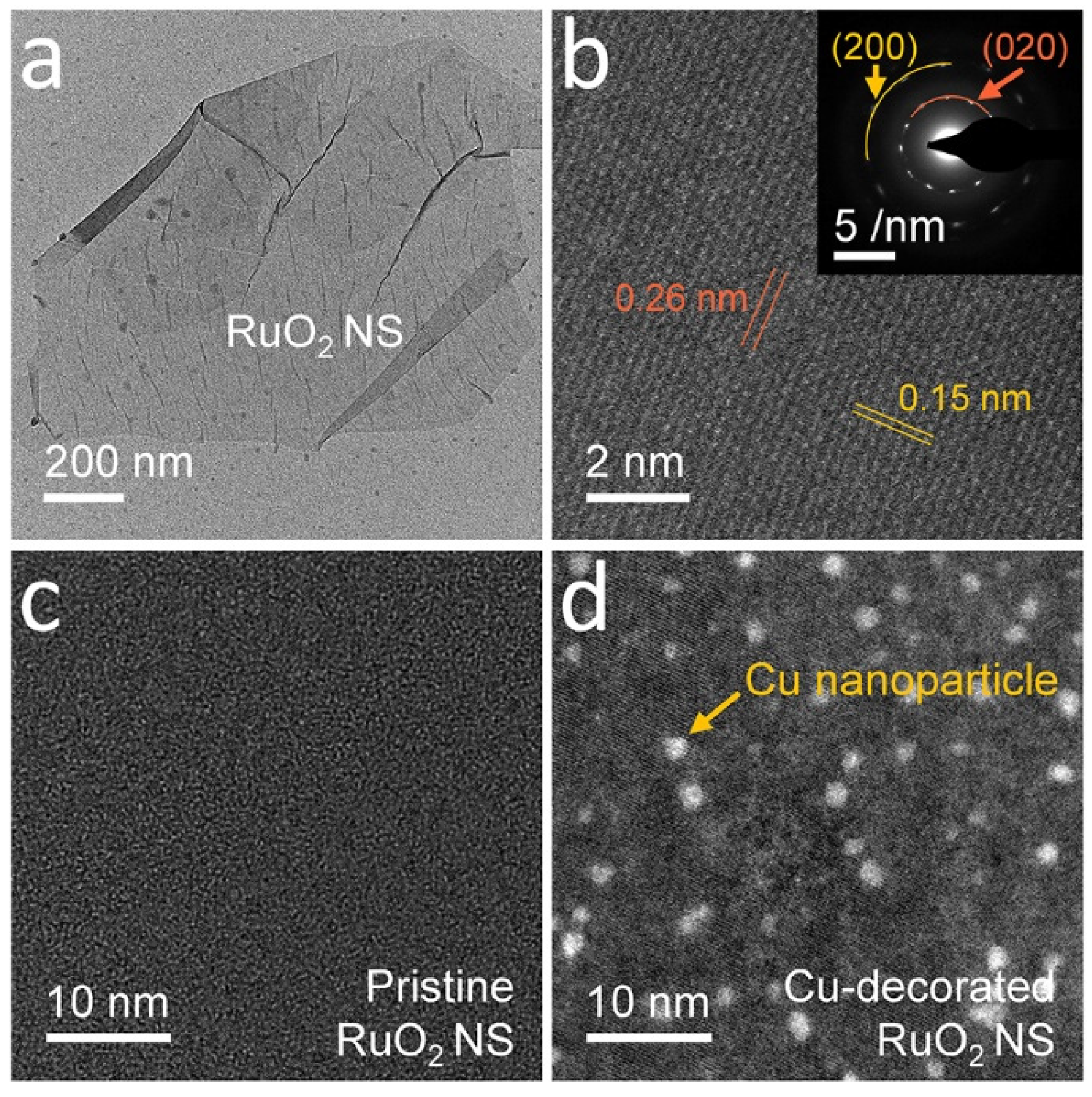
Abstract
:1. Introduction
2. Materials and Methods
2.1. Materilas
2.2. Metal Nanoparticle Surface Decorations
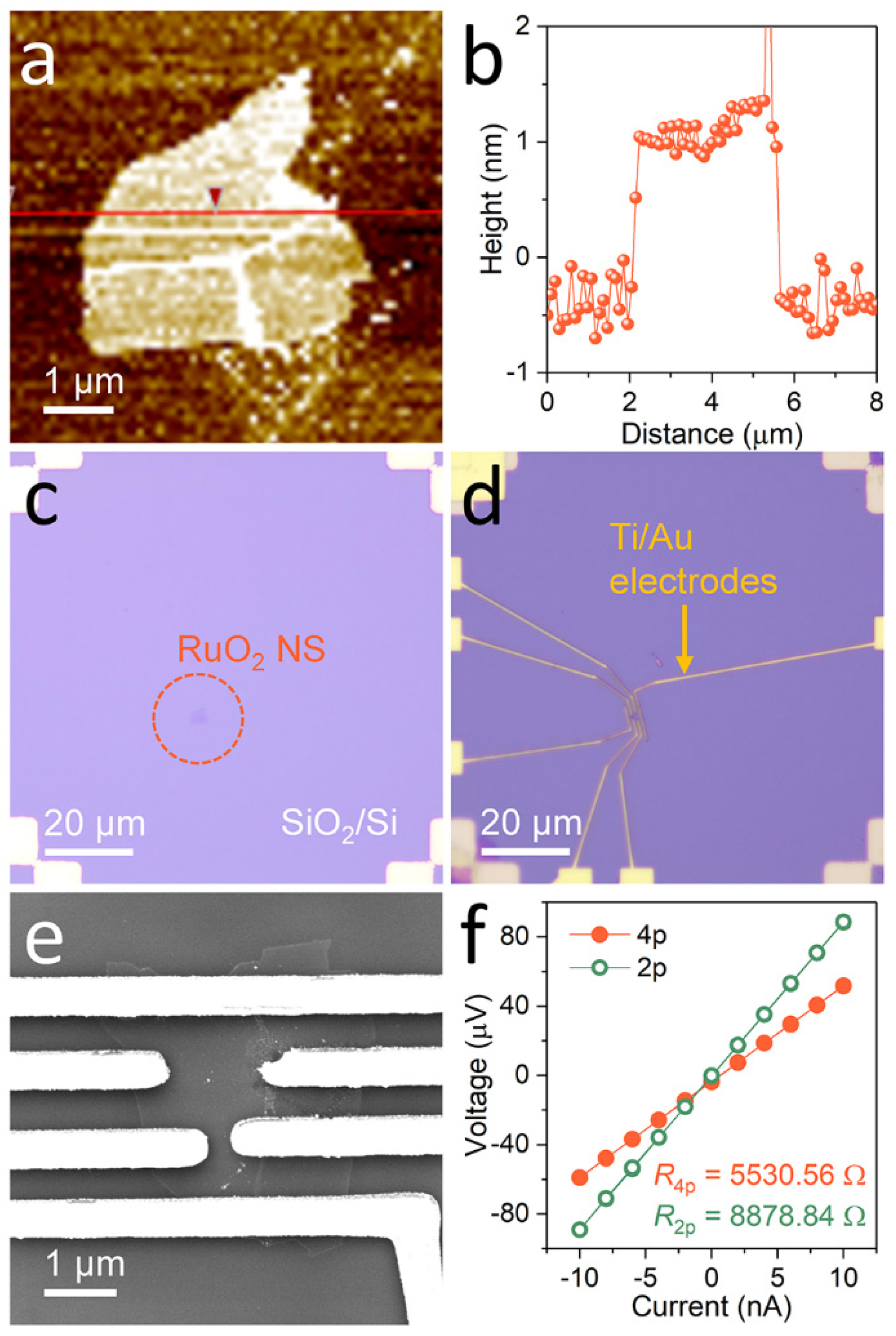
2.3. Device Fabrication
2.4. Measurement Techniques

3. Results and Discussion
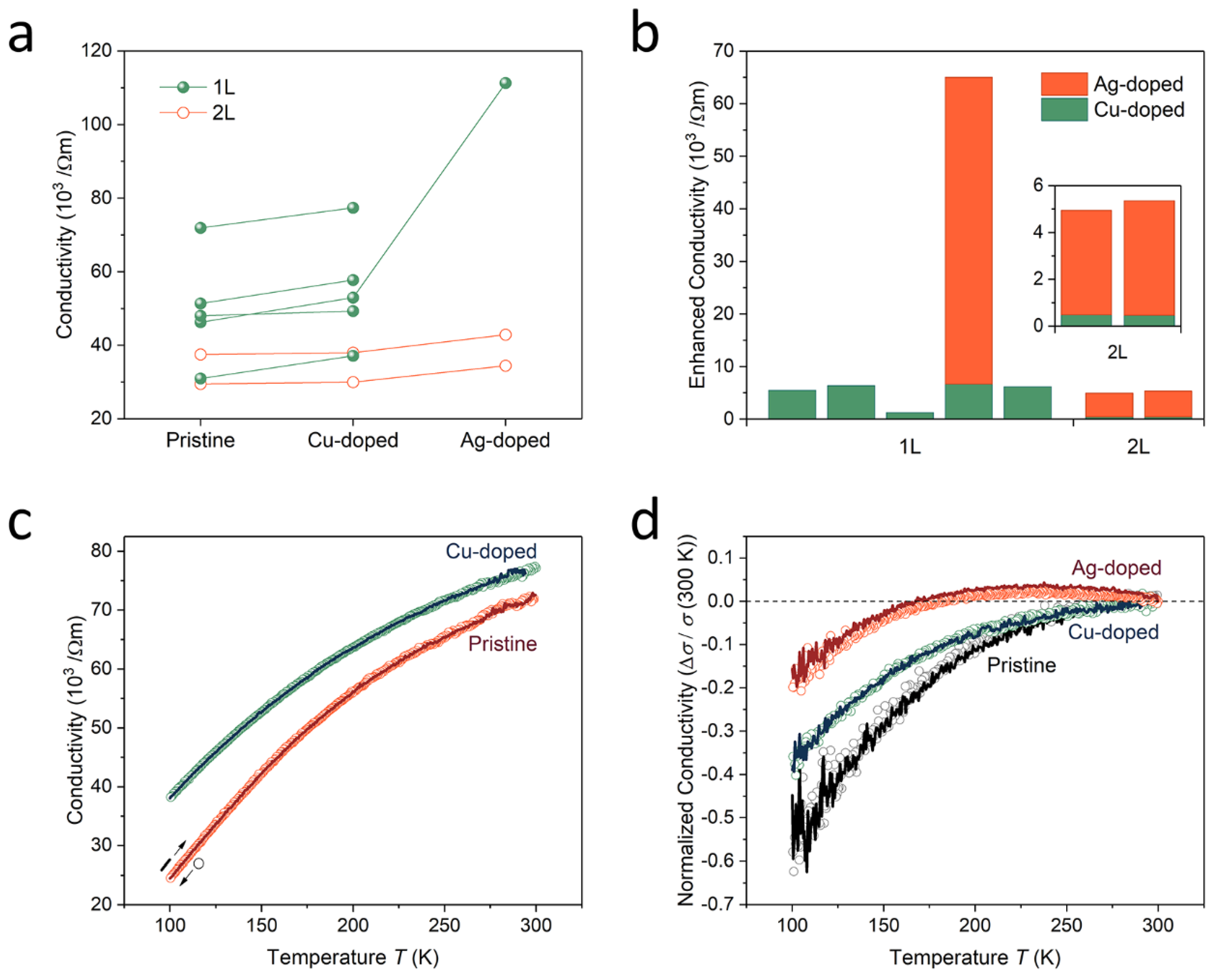
3.1. Increase in Electrical Conductivity
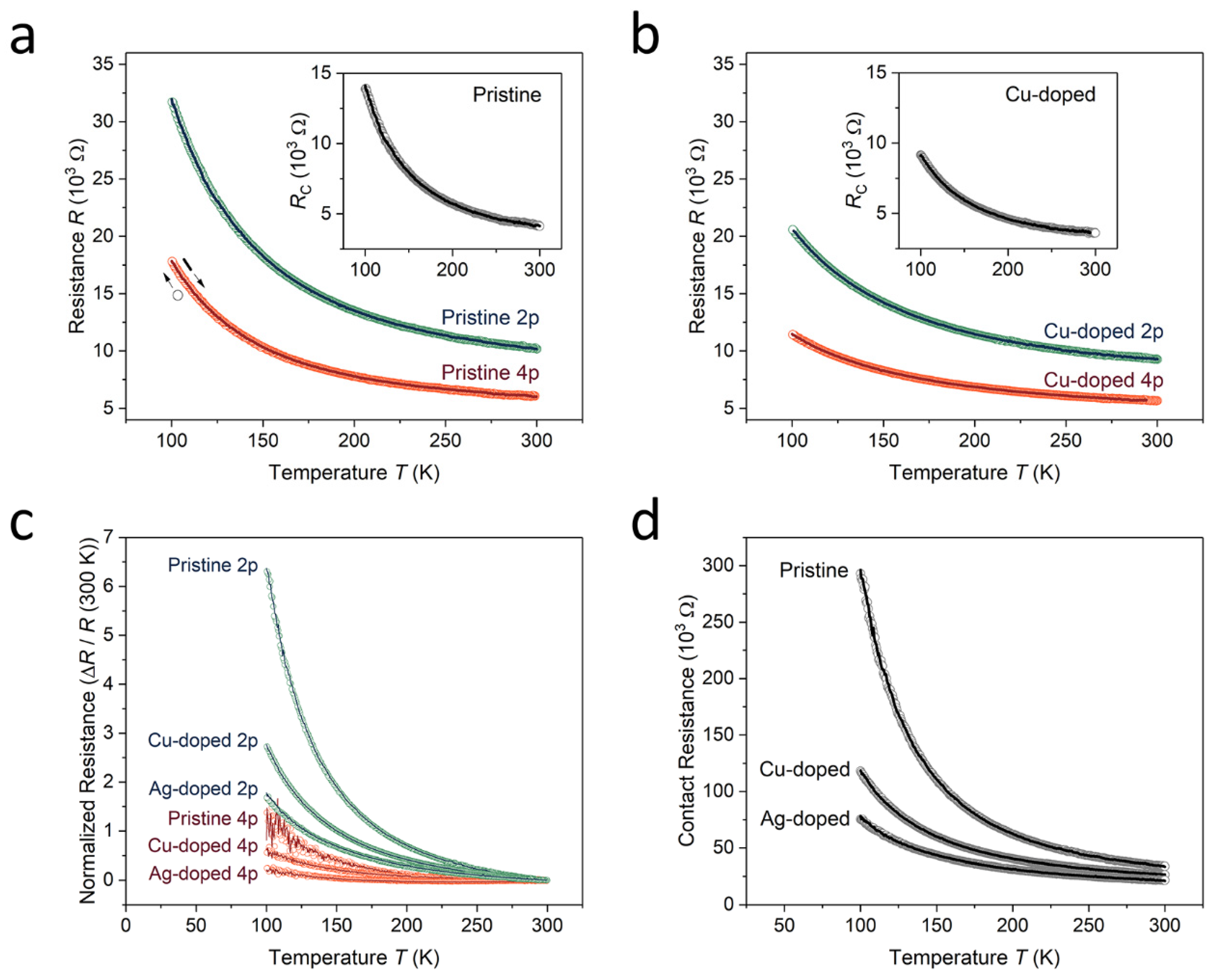
3.2. Contact Resistance
4. Conclusions
Author Contributions
Funding
Data Availability Statement
Conflicts of Interest
References
- Novoselov, K.S.; Geim, A.K.; Morozov, S.V.; Jiang, D.; Katsnelson, M.I.; Grigorieva, I.V.; Dubonos, S.V.; Firsov, A.A. Two-dimensional gas of massless Dirac fermions in graphene. Nature 2005, 438, 197–200. [Google Scholar] [CrossRef] [PubMed]
- Geim, A.K.; Novoselov, K.S. The rise of graphene. Nat. Mater. 2007, 6, 183–191. [Google Scholar] [CrossRef] [PubMed]
- Osada, M.; Sasaki, T. Two-Dimensional Dielectric Nanosheets: Novel Nanoelectronics from Nanocrystal Building Blocks. Adv. Mater. 2012, 24, 210–228. [Google Scholar] [CrossRef] [PubMed]
- Wang, Q.H.; Kalantar-Zadeh, K.; Kis, A.; Coleman, J.N.; Strano, M.S. Electronics and optoelectronics of two-dimensional transition metal dichalcogenides. Nat. Nano 2012, 7, 699–712. [Google Scholar] [CrossRef]
- Cao, A.; Liu, Z.; Chu, S.; Wu, M.; Ye, Z.; Cai, Z.; Chang, Y.; Wang, S.; Gong, Q.; Liu, Y. A Facile One-step Method to Produce Graphene–CdS Quantum Dot Nanocomposites as Promising Optoelectronic Materials. Adv. Mater. 2010, 22, 103–106. [Google Scholar] [CrossRef]
- Zhang, H.; Lu, S.B.; Zheng, J.; Du, J.; Wen, S.C.; Tang, D.Y.; Loh, K.P. Molybdenum disulfide (MoS2) as a broadband saturable absorber for ultra-fast photonics. Opt. Express 2014, 22, 7249–7260. [Google Scholar] [CrossRef]
- Lee, G.-H.; Yu, Y.-J.; Cui, X.; Petrone, N.; Lee, C.-H.; Choi, M.S.; Lee, D.-Y.; Lee, C.; Yoo, W.J.; Watanabe, K.; et al. Flexible and Transparent MoS2 Field-Effect Transistors on Hexagonal Boron Nitride-Graphene Heterostructures. ACS Nano 2013, 7, 7931–7936. [Google Scholar] [CrossRef]
- He, Q.; Zeng, Z.; Yin, Z.; Li, H.; Wu, S.; Huang, X.; Zhang, H. Fabrication of Flexible MoS2 Thin-Film Transistor Arrays for Practical Gas-Sensing Applications. Small 2012, 8, 2994–2999. [Google Scholar] [CrossRef]
- Radisavljevic, B.; Radenovic, A.; Brivio, J.; Giacometti, V.; Kis, A. Single-layer MoS2 transistors. Nat. Nano 2011, 6, 147–150. [Google Scholar] [CrossRef]
- Voiry, D.; Yamaguchi, H.; Li, J.; Silva, R.; Alves, D.C.B.; Fujita, T.; Chen, M.; Asefa, T.; Shenoy, V.B.; Eda, G.; et al. Enhanced catalytic activity in strained chemically exfoliated WS2 nanosheets for hydrogen evolution. Nat. Mater. 2013, 12, 850–855. [Google Scholar] [CrossRef]
- Pletikosić, I.; Ali, M.N.; Fedorov, A.V.; Cava, R.J.; Valla, T. Electronic Structure Basis for the Extraordinary Magnetoresistance in WTe2. Phys. Rev. Lett. 2014, 113, 216601. [Google Scholar] [CrossRef] [PubMed] [Green Version]
- Zhang, Y.; Chang, T.-R.; Zhou, B.; Cui, Y.-T.; Yan, H.; Liu, Z.; Schmitt, F.; Lee, J.; Moore, R.; Chen, Y.; et al. Direct observation of the transition from indirect to direct bandgap in atomically thin epitaxial MoSe2. Nat. Nano 2014, 9, 111–115. [Google Scholar] [CrossRef]
- Wickramaratne, D.; Zahid, F.; Lake, R.K. Electronic and thermoelectric properties of few-layer transition metal dichalcogenides. J. Chem. Phys. 2014, 140, 124710. [Google Scholar] [CrossRef] [Green Version]
- Li, L.; Yu, Y.; Ye, G.J.; Ge, Q.; Ou, X.; Wu, H.; Feng, D.; Chen, X.H.; Zhang, Y. Black phosphorus field-effect transistors. Nat. Nano 2014, 9, 372–377. [Google Scholar] [CrossRef] [PubMed] [Green Version]
- Xia, F.; Wang, H.; Jia, Y. Rediscovering black phosphorus as an anisotropic layered material for optoelectronics and electronics. Nat. Commun. 2014, 5, 4458. [Google Scholar] [CrossRef] [Green Version]
- Fei, R.; Faghaninia, A.; Soklaski, R.; Yan, J.-A.; Lo, C.; Yang, L. Enhanced Thermoelectric Efficiency via Orthogonal Electrical and Thermal Conductances in Phosphorene. Nano Lett. 2014, 14, 6393–6399. [Google Scholar] [CrossRef] [Green Version]
- Watanabe, K.; Taniguchi, T.; Kanda, H. Direct-bandgap properties and evidence for ultraviolet lasing of hexagonal boron nitride single crystal. Nat. Mater. 2004, 3, 404–409. [Google Scholar] [CrossRef] [PubMed]
- Song, L.; Ci, L.; Lu, H.; Sorokin, P.B.; Jin, C.; Ni, J.; Kvashnin, A.G.; Kvashnin, D.G.; Lou, J.; Yakobson, B.I.; et al. Large Scale Growth and Characterization of Atomic Hexagonal Boron Nitride Layers. Nano Lett. 2010, 10, 3209–3215. [Google Scholar] [CrossRef]
- Gao, S.; Lin, Y.; Jiao, X.; Sun, Y.; Luo, Q.; Zhang, W.; Li, D.; Yang, J.; Xie, Y. Partially oxidized atomic cobalt layers for carbon dioxide electroreduction to liquid fuel. Nature 2016, 529, 68–71. [Google Scholar] [CrossRef]
- Akhavan, O.; Ghaderi, E. Photocatalytic Reduction of Graphene Oxide Nanosheets on TiO2 Thin Film for Photoinactivation of Bacteria in Solar Light Irradiation. J. Phys. Chem. C 2009, 113, 20214–20220. [Google Scholar] [CrossRef]
- Hu, C.-C.; Chang, K.-H.; Lin, M.-C.; Wu, Y.-T. Design and Tailoring of the Nanotubular Arrayed Architecture of Hydrous RuO2 for Next Generation Supercapacitors. Nano Lett. 2006, 6, 2690–2695. [Google Scholar] [CrossRef] [PubMed]
- Wu, Z.-S.; Zhou, G.; Yin, L.-C.; Ren, W.; Li, F.; Cheng, H.-M. Graphene/metal oxide composite electrode materials for energy storage. Nano Energy 2012, 1, 107–131. [Google Scholar] [CrossRef]
- Yang, X.-y.; Xu, J.-j.; Bao, D.; Chang, Z.-w.; Liu, D.-p.; Zhang, Y.; Zhang, X.-B. High-Performance Integrated Self-Package Flexible Li–O2 Battery Based on Stable Composite Anode and Flexible Gas Diffusion Layer. Adv. Mater. 2017, 29, 1700378. [Google Scholar] [CrossRef]
- Liu, T.; Xu, J.-J.; Liu, Q.-C.; Chang, Z.-W.; Yin, Y.-B.; Yang, X.-Y.; Zhang, X.-B. Ultrathin, Lightweight, and Wearable Li-O2 Battery with High Robustness and Gravimetric/Volumetric Energy Density. Small 2017, 13, 1602952. [Google Scholar] [CrossRef] [PubMed]
- Wang, C.; Osada, M.; Ebina, Y.; Li, B.-W.; Akatsuka, K.; Fukuda, K.; Sugimoto, W.; Ma, R.; Sasaki, T. All-Nanosheet Ultrathin Capacitors Assembled Layer-by-Layer via Solution-Based Processes. ACS Nano 2014, 8, 2658–2666. [Google Scholar] [CrossRef] [PubMed]
- Lee, S.; Jin, X.; Kim, I.Y.; Gu, T.-H.; Choi, J.-W.; Nahm, S.; Hwang, S.-J. Superior Additive of Exfoliated RuO2 Nanosheet for Optimizing the Electrode Performance of Metal Oxide over Graphene. J. Phys. Chem. C 2016, 120, 11786–11796. [Google Scholar] [CrossRef]
- Choi, S.-J.; Jang, J.-S.; Park, H.J.; Kim, I.-D. NO2 Sensors: Optically Sintered 2D RuO2 Nanosheets: Temperature-Controlled NO2 Reaction. Adv. Funct. Mater. 2017, 27, 1606026. [Google Scholar] [CrossRef]
- Ko, D.-S.; Lee, W.-J.; Sul, S.; Jung, C.; Yun, D.-J.; Kim, H.-G.; Son, W.-J.; Chung, J.G.; Jung, D.W.; Kim, S.Y.; et al. Understanding the structural, electrical, and optical properties of monolayer h-phase RuO2 nanosheets: A combined experimental and computational study. NPG Asia Mater. 2018, 10, 266–276. [Google Scholar] [CrossRef]
- Yoo, S.; Kim, J.; Moon, H.; Kim, S.Y.; Ko, D.S.; Shin, W.H.; Hwang, S.; Jung, D.W.; Sul, S.; Kwak, C.; et al. Strong enhancement of electrical conductivity in two-dimensional micrometer-sized RuO2 nanosheets for flexible transparent electrodes. Nanoscale 2017, 9, 7104–7113. [Google Scholar] [CrossRef]
- Kim, J.; Yoo, S.; Moon, H.; Kim, S.Y.; Ko, D.S.; Roh, J.W.; Lee, W. Ambipolar thermoelectric power of chemically-exfoliated RuO2 nanosheets. Nanotechnology 2018, 29, 015404. [Google Scholar] [CrossRef] [Green Version]
- Kim, S.Y.; Shin, W.H.; Jung, D.W.; Ko, D.-S.; Roh, J.W.; Hwang, S.; Lee, J.; Lee, K.; Park, H.J.; Kwak, C.; et al. Facile and accelerated production of RuO2 monolayers via a dual-step intercalation process. Inorg. Chem. Front. 2020, 7, 1445–1450. [Google Scholar] [CrossRef]
- Kim, J.; Lee, S.; Brovman, Y.M.; Kim, P.; Lee, W. Diameter-dependent thermoelectric figure of merit in single-crystalline Bi nanowires. Nanoscale 2015, 7, 5053–5059. [Google Scholar] [CrossRef] [PubMed] [Green Version]
- Moon, H.; Bang, J.; Hong, S.; Kim, G.; Roh, J.W.; Kim, J.; Lee, W. Strong Thermopower Enhancement and Tunable Power Factor via Semimetal to Semiconductor Transition in a Transition-Metal Dichalcogenide. ACS Nano 2019, 13, 13317–13324. [Google Scholar] [CrossRef] [PubMed]


Publisher’s Note: MDPI stays neutral with regard to jurisdictional claims in published maps and institutional affiliations. |
© 2021 by the authors. Licensee MDPI, Basel, Switzerland. This article is an open access article distributed under the terms and conditions of the Creative Commons Attribution (CC BY) license (https://creativecommons.org/licenses/by/4.0/).
Share and Cite
Kim, J.; Youn, S.; Baek, J.Y.; Kim, D.H.; Kim, S.; Lee, W.; Park, H.J.; Kim, J.; Chun, D.W.; Park, S.-S.; et al. Modulation of Conductivity and Contact Resistance of RuO2 Nanosheets via Metal Nano-Particles Surface Decoration. Nanomaterials 2021, 11, 2444. https://doi.org/10.3390/nano11092444
Kim J, Youn S, Baek JY, Kim DH, Kim S, Lee W, Park HJ, Kim J, Chun DW, Park S-S, et al. Modulation of Conductivity and Contact Resistance of RuO2 Nanosheets via Metal Nano-Particles Surface Decoration. Nanomaterials. 2021; 11(9):2444. https://doi.org/10.3390/nano11092444
Chicago/Turabian StyleKim, Jongwon, Seonhye Youn, Ju Young Baek, Dong Hwan Kim, Sumin Kim, Wooyoung Lee, Hee Jung Park, Juyoung Kim, Dong Won Chun, Sang-Shik Park, and et al. 2021. "Modulation of Conductivity and Contact Resistance of RuO2 Nanosheets via Metal Nano-Particles Surface Decoration" Nanomaterials 11, no. 9: 2444. https://doi.org/10.3390/nano11092444