
Anisotropic Optical Response of WTe2 Single Crystals Studied by Ellipsometric Analysis

 ,
,  , , and
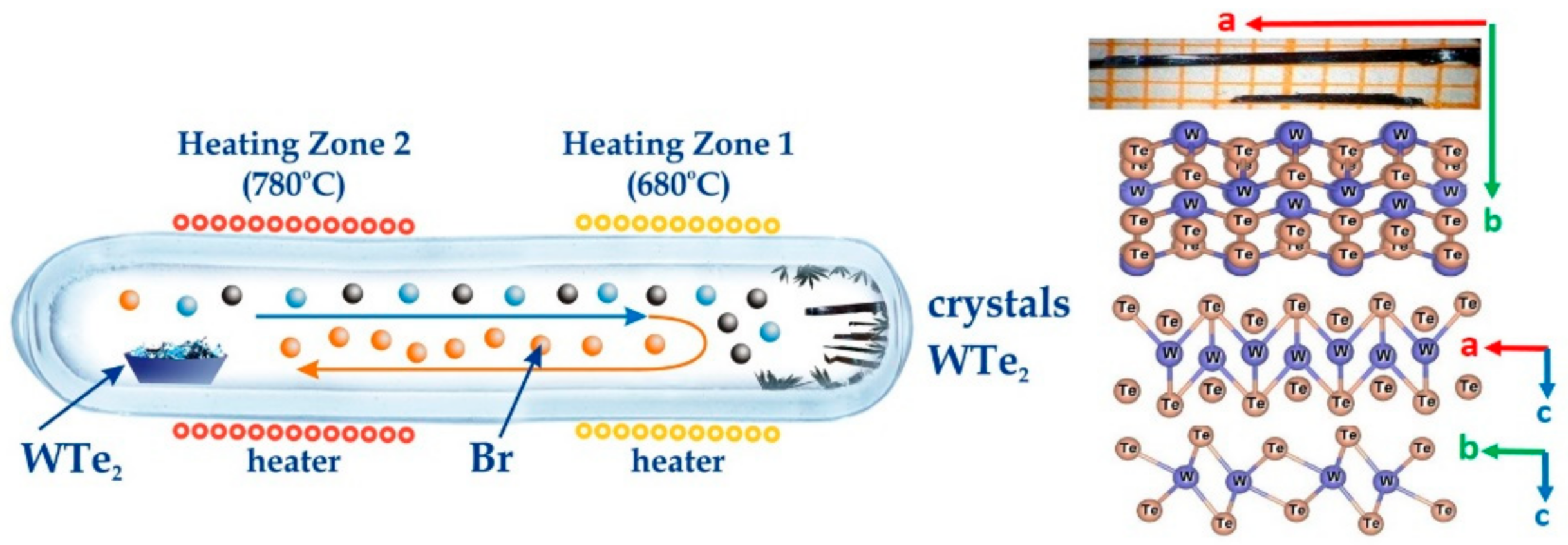
Abstract
:1. Introduction
2. Materials, Methods and Experimental Details
2.1. WTe2 Crystal Growth Procedure Using the CVT Method
2.2. Characterization Instruments and Techniques
3. Discussion and Results
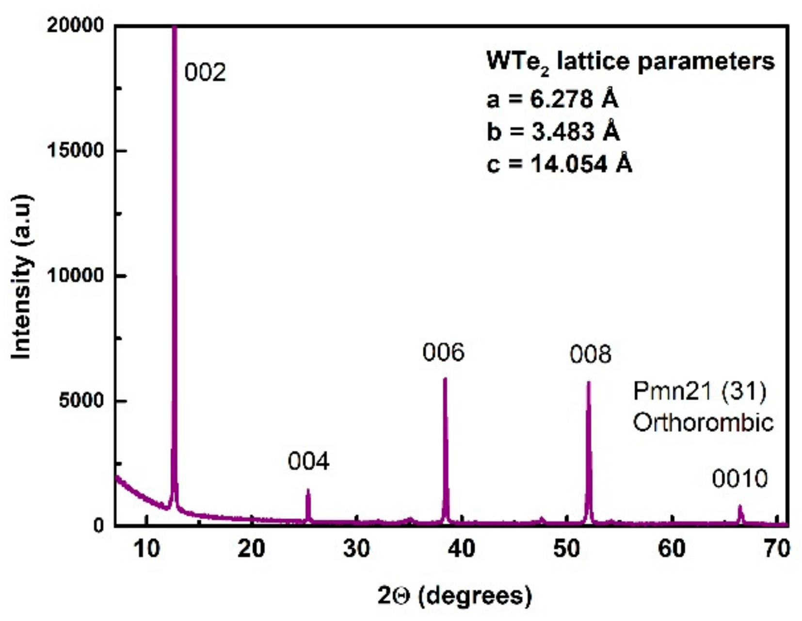
3.1. XRD Analysis
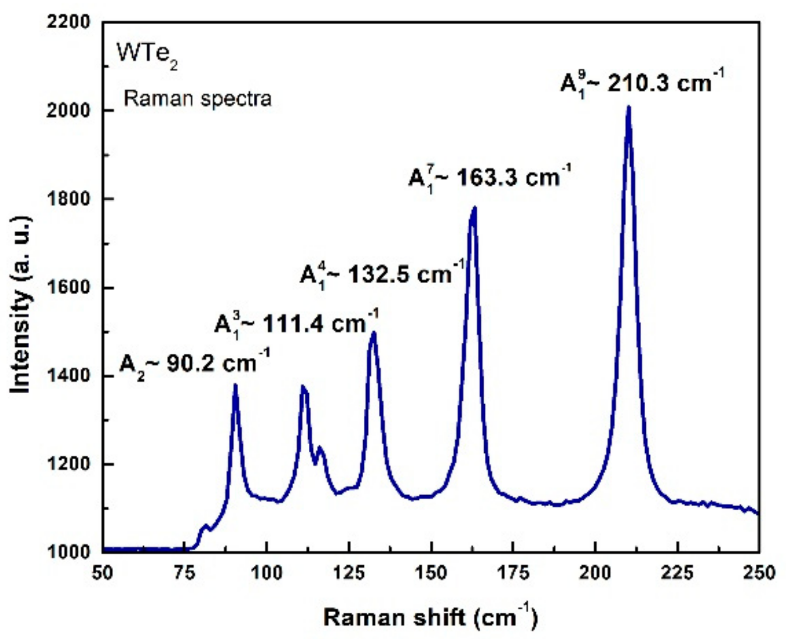
3.2. Raman Spectroscopy
3.3. Spectroscopic Ellipsometry
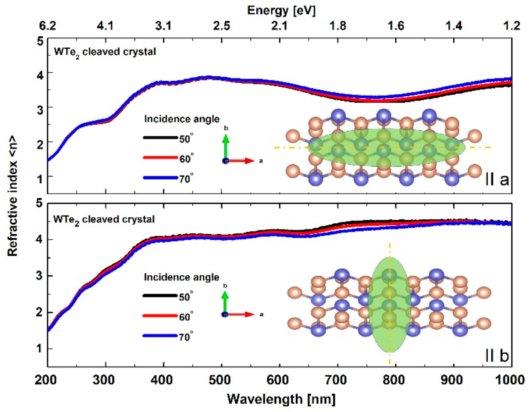
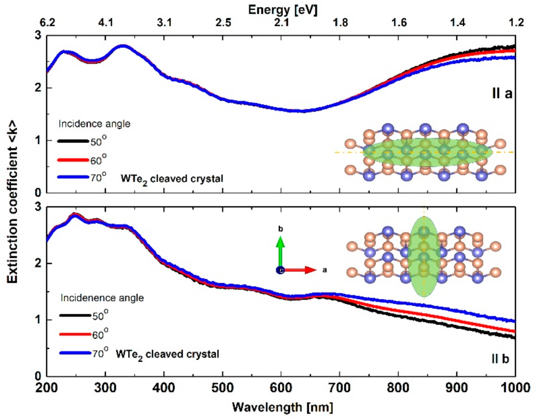
3.3.1. Basic Isotropic Model Approach: Refractive Index and Extinction Coefficient
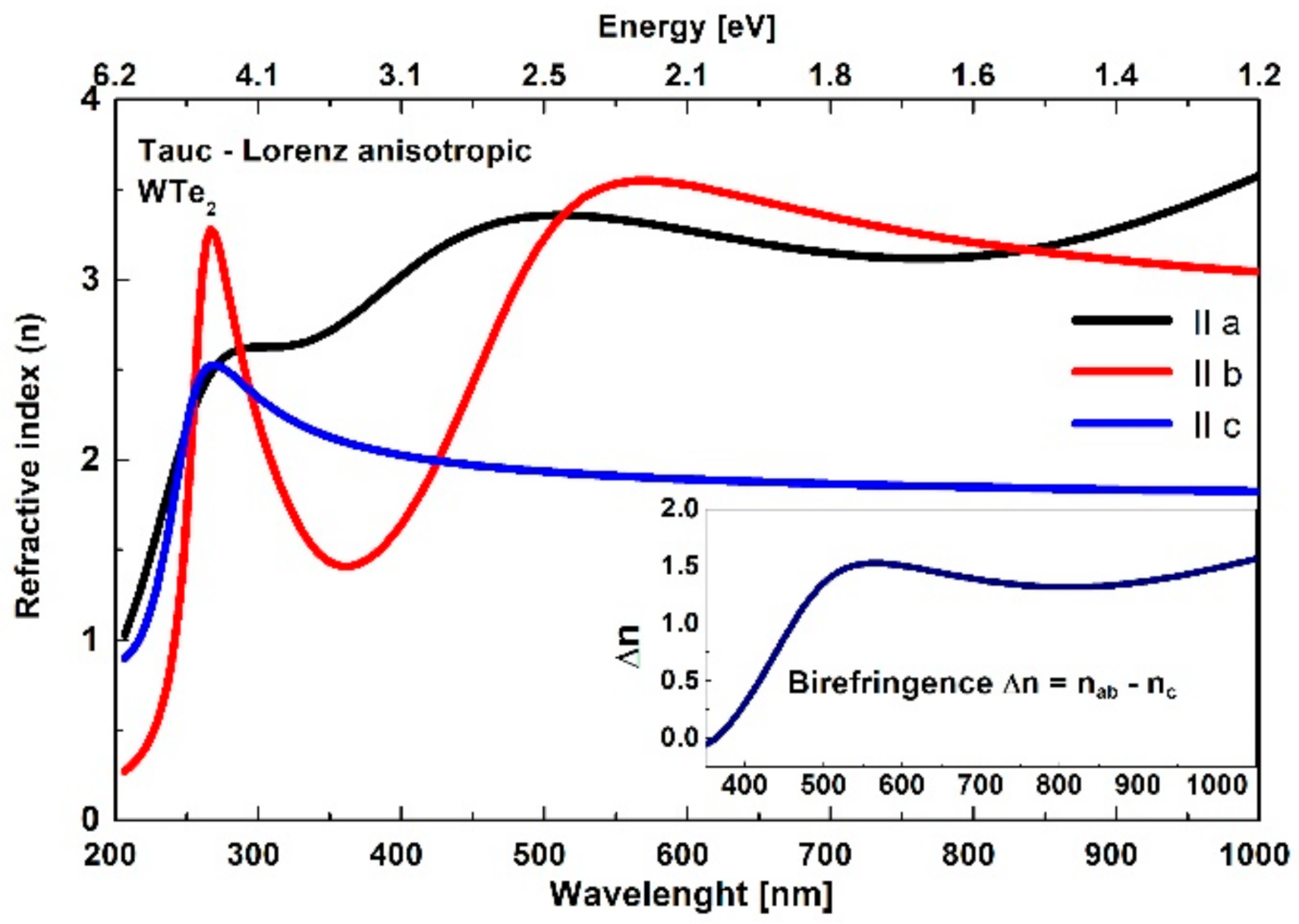
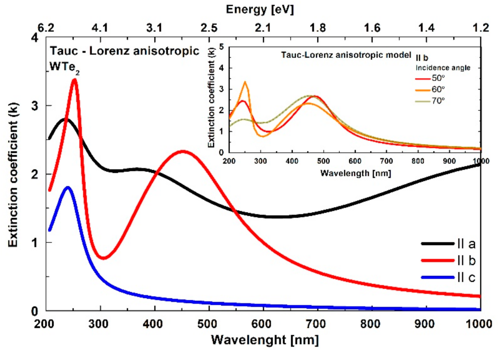
3.3.2. Tauc–Lorentz Oscillator Model: Refractive Index and Extinction Coefficient
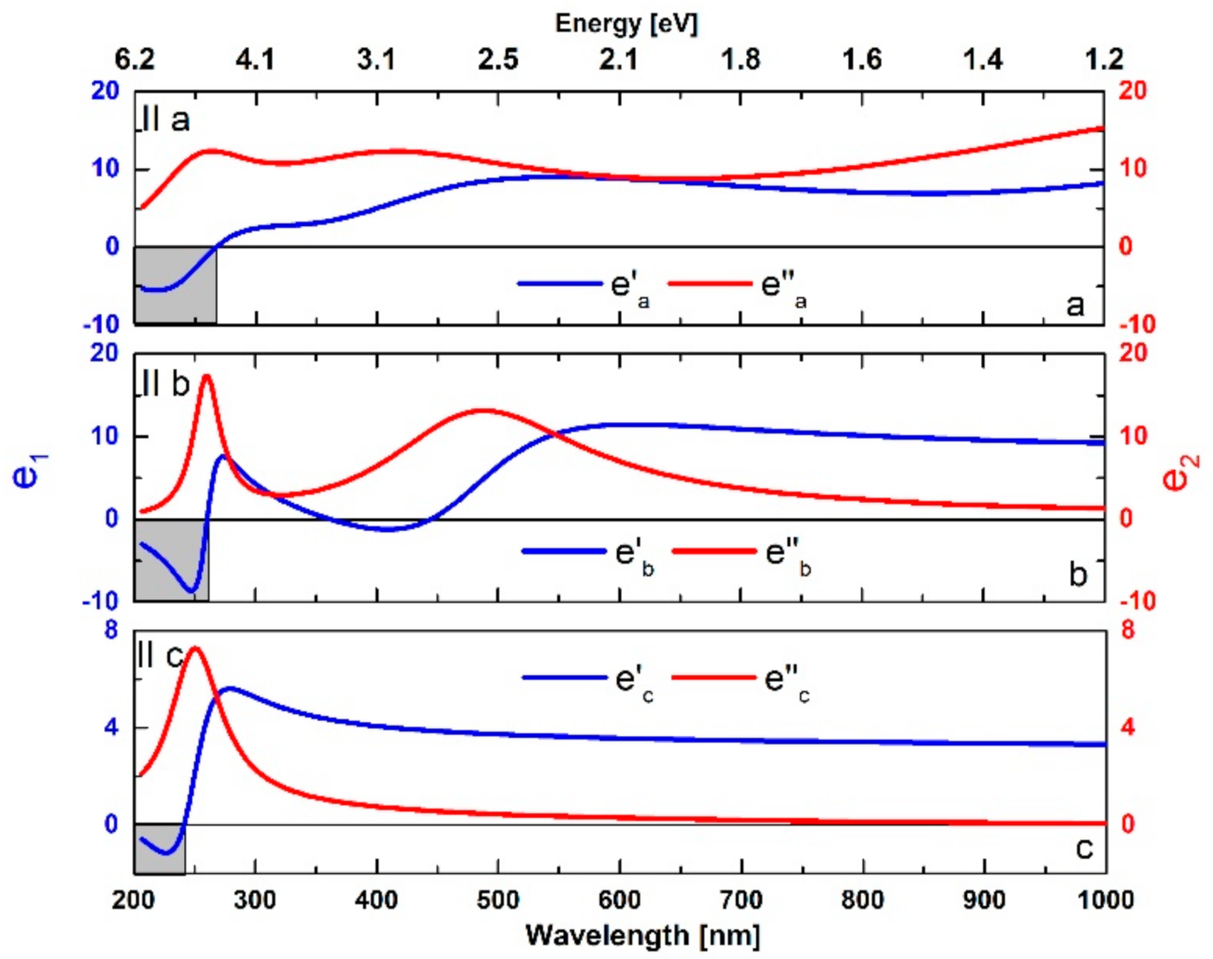
3.3.3. Dielectric Functions
4. Conclusions
- High values of the refractive index (~4) were observed for both models, especially in the visible/near-infrared spectral range. The influence of the optical anisotropy was also well detected with the simplistic isotropic modeling, with observed distinct differences in the optical constants ( and ) depending on the in-plane crystallographic orientations.
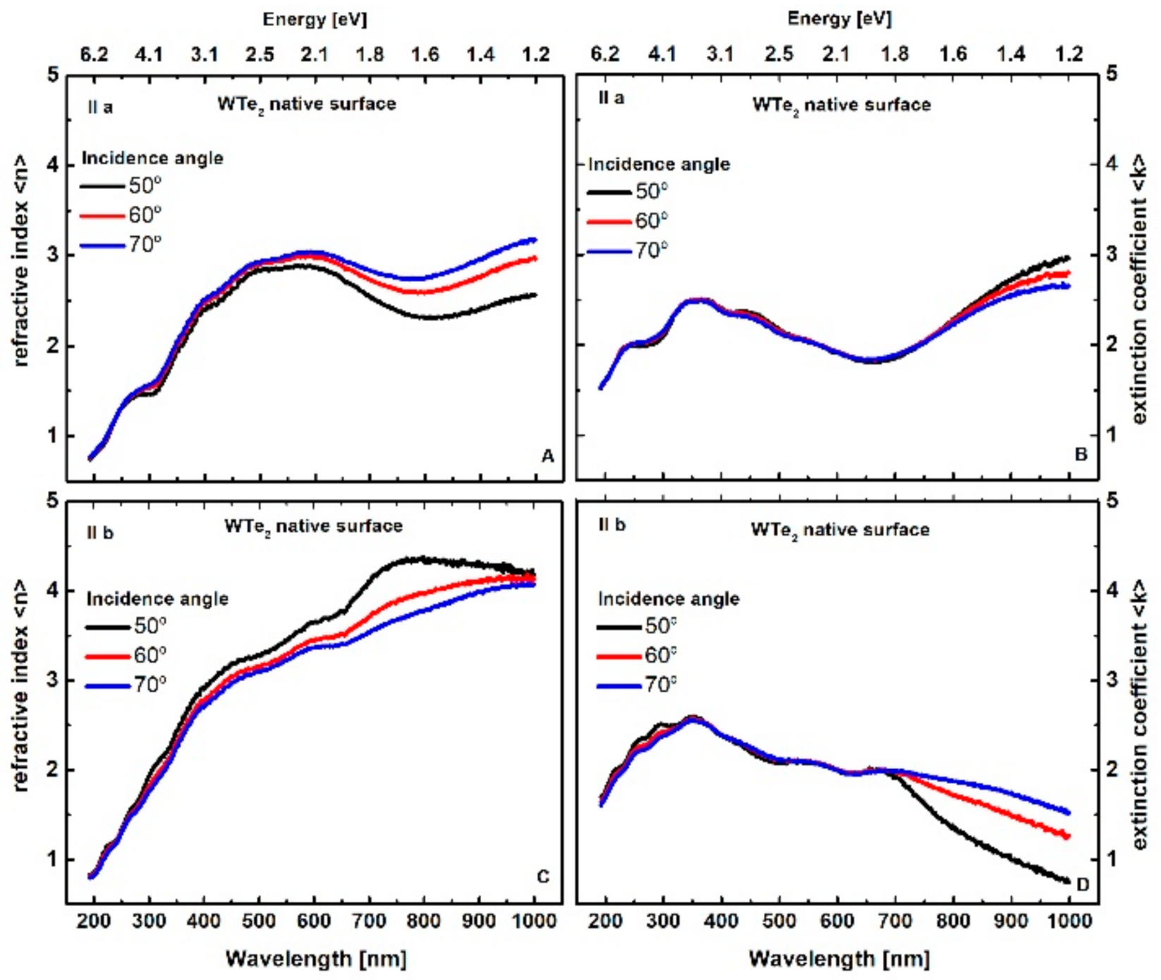
- Identical anisotropic tendencies of the intrinsic WTe2 spectral behavior were also observed for the native crystal surface, which is expected to be affected by the formation of an oxide surface layer (Appendix A).
- The calculated dispersions of the refractive index and extinction coefficient in the frames of the Tauc–Lorentz oscillator model indicate the tri-axial nature of the optical response.
- The extrapolated band gap values of 0.006 and 0.273 eV in the a and b directions, respectively, are in good agreement with those determined by energy band structure calculations in the literature.
- The real component of the dielectric function shows negative values, which also indicates surface plasmon polariton activity.
Author Contributions
Funding
Institutional Review Board Statement
Informed Consent Statement
Data Availability Statement
Acknowledgments
Conflicts of Interest
Appendix A
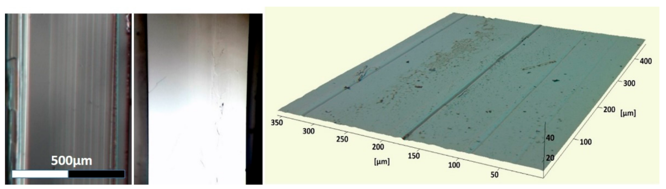
Appendix A.1. Optical Imaging and Profilometry

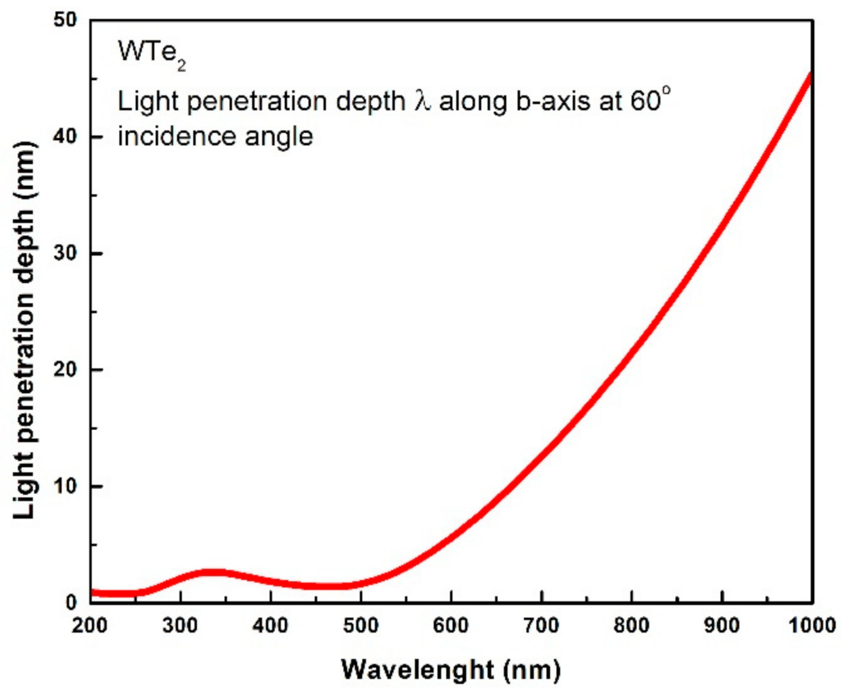
Appendix A.2. Ellipsometric Analysis: Native Surface and Light Penetration Depth


References
- Lee, C.H.; Silva, E.C.; Calderin, L.; Nguyen, M.A.T.; Hollander, M.J.; Bersch, B.; Mallouk, T.E.; Robinson, J.A. Tungsten Ditelluride: A layered semimetal. Sci. Rep. 2015, 5, 10013. [Google Scholar] [CrossRef]
- Tian, W.; Yu, W.; Liu, X.; Wang, Y.; Shi, J. A Review of the Characteristics, Synthesis, and Thermodynamics of Type-II Weyl Semimetal WTe2. Materials 2018, 11, 1185. [Google Scholar] [CrossRef] [Green Version]
- Pan, X.-C.; Wang, X.; Song, F.; Wang, B. The study on quantum material WTe2. Adv. Phys. X 2018, 3, 1468279. [Google Scholar] [CrossRef]
- Das, P.K.; Di Sante, D.; Cilento, F.; Bigi, C.; Kopic, D.; Soranzio, D.; Sterzi, A.; Krieger, J.A.; Vobornik, I.; Fujii, J.; et al. Electronic properties of type-II Weyl semimetal WTe2. A review perspective. arXiv 2018, 1, 014003. [Google Scholar]
- Jia, Z.Y.; Song, Y.H.; Li, X.B.; Ran, K.; Lu, P.; Zheng, H.J.; Zhu, X.Y.; Shi, Z.Q.; Sun, J.; Wen, J.; et al. Direct visualization of a two-dimensional topological insulator in the single-layer 1T′-WTe2. Phys. Rev. B 2017, 96, 041108. [Google Scholar] [CrossRef] [Green Version]
- Fei, Z.; Palomaki, T.; Wu, S.; Zhao, W.; Cai, X.; Sun, B.; Nguyen, P.; Finney, J.; Xu, X.; Cobden, D.H. Edge conduction in monolayer WTe2. Nat. Phys. 2017, 13, 677–682. [Google Scholar] [CrossRef] [Green Version]
- Xu, S.Y.; Ma, Q.; Shen, H.; Fatemi, V.; Wu, S.; Chang, T.R.; Chang, G.; Valdivia, A.M.M.; Chan, C.K.; Gibson, Q.D.; et al. Electrically switchable Berry curvature dipole in the monolayer topological insulator WTe2. Nat. Phys. 2018, 14, 900–906. [Google Scholar] [CrossRef]
- Jelver, L.; Stradi, D.; Stokbro, K.; Olsen, T.; Jacobsen, K.W. Spontaneous breaking of time-reversal symmetry at the edges of 1T′ monolayer transition metal dichalcogenides. Phys. Rev. B 2019, 99, 155420. [Google Scholar] [CrossRef] [Green Version]
- Augustin, J.; Eyert, V.; Böker, T.; Frentrup, W.; Dwelk, H.; Janowitz, C.; Manzke, R. Electronic band structure of the layered compound Td-WTe2. Phys. Rev. B Condens. Matter Mater. Phys. 2000, 62, 10812–10823. [Google Scholar] [CrossRef] [Green Version]
- Zhang, Q.; Zhang, R.; Chen, J.; Shen, W.; An, C.; Hu, X.; Dong, M.; Liu, J.; Zhu, L. Remarkable electronic and optical anisotropy of layered 1T’-WTe2 2D materials. Beilstein J. Nanotechnol. 2019, 10, 1745–1753. [Google Scholar] [CrossRef] [Green Version]
- Frenzel, A.J.; Homes, C.C.; Gibson, Q.D.; Shao, Y.M.; Post, K.W.; Charnukha, A.; Cava, R.J.; Basov, D.N. Anisotropic electrodynamics of type-II Weyl semimetal candidate WTe2. Phys. Rev. B 2017, 95, 245140. [Google Scholar] [CrossRef] [Green Version]
- Ali, M.N.; Xiong, J.; Flynn, S.; Tao, J.; Gibson, Q.D.; Schoop, L.M.; Liang, T.; Haldolaarachchige, N.; Hirschberger, M.; Ong, N.P.; et al. Large, non-saturating magnetoresistance in WTe2. Nature 2014, 514, 205–208. [Google Scholar] [CrossRef] [PubMed] [Green Version]
- Zhang, E.; Chen, R.; Huang, C.; Yu, J.; Zhang, K.; Wang, W.; Liu, S.; Ling, J.; Wan, X.; Lu, H.Z.; et al. Tunable Positive to Negative Magnetoresistance in Atomically Thin WTe2. Nano Lett. 2017, 17, 878–885. [Google Scholar] [CrossRef]
- Sharma, P.; Xiang, F.X.; Shao, D.F.; Zhang, D.; Tsymbal, E.Y.; Hamilton, A.R.; Seidel, J. A room-temperature ferroelectric semimetal. Sci. Adv. 2019, 5, eaax5080. [Google Scholar] [CrossRef] [PubMed] [Green Version]
- Kang, D.; Zhou, Y.; Yi, W.; Yang, C.; Guo, J.; Shi, Y.; Zhang, S.; Wang, Z.; Zhang, C.; Jiang, S.; et al. Superconductivity emerging from a suppressed large magnetoresistant state in tungsten ditelluride. Nat. Commun. 2015, 6, 7804. [Google Scholar] [CrossRef] [Green Version]
- Wu, Y.; Jo, N.H.; Ochi, M.; Huang, L.; Mou, D.; Bud’Ko, S.L.; Canfield, P.; Trivedi, N.; Arita, R.; Kaminski, A. Temperature-Induced Lifshitz Transition in WTe2. Phys. Rev. Lett. 2015, 115, 166602. [Google Scholar] [CrossRef] [Green Version]
- Zhu, Z.; Lin, X.; Liu, J.; Fauqué, B.; Tao, Q.; Yang, C.; Shi, Y.; Behnia, K. Quantum oscillations, thermoelectric coefficients, and the fermi surface of semimetallic WTe2. Phys. Rev. Lett. 2015, 114, 176601. [Google Scholar] [CrossRef] [Green Version]
- Tang, S.; Zhang, C.; Wong, D.; Pedramrazi, Z.; Tsai, H.Z.; Jia, C.; Moritz, B.; Claassen, M.; Ryu, H.; Kahn, S.; et al. Quantum spin Hall state in monolayer 1T’-WTe 2. Nat. Phys. 2017, 13, 683–687. [Google Scholar] [CrossRef]
- Xia, F.; Wang, H.; Xiao, D.; Dubey, M.; Ramasubramaniam, A. Two-dimensional material nanophotonics. Nat. Photonics 2014, 8, 899–907. [Google Scholar] [CrossRef]
- Reserbat-Plantey, A.; Epstein, I.; Torre, I.; Costa, A.T.; Gonçalves, P.A.D.; Mortensen, N.A.; Polini, M.; Song, J.C.W.; Peres, N.M.R.; Koppens, F.H.L. Quantum Nanophotonics in Two-Dimensional Materials. ACS Photonics 2021, 8, 85–101. [Google Scholar] [CrossRef]
- Ling, H.; Li, R.; Davoyan, A.R. All van der Waals Integrated Nanophotonics with Bulk Transition Metal Dichalcogenides. ACS Photonics 2021, 8, 721–730. [Google Scholar] [CrossRef]
- Ermolaev, G.A.; Grudinin, D.V.; Stebunov, Y.V.; Voronin, K.V.; Kravets, V.G.; Duan, J.; Mazitov, A.B.; Tselikov, G.I.; Bylinkin, A.; Yakubovsky, D.I.; et al. Giant optical anisotropy in transition metal dichalcogenides for next-generation photonics. Nat. Commun. 2021, 12, 854. [Google Scholar] [CrossRef]
- Green, T.D.; Baranov, D.G.; Munkhbat, B.; Verre, R.; Shegai, T.; Käll, M. Optical material anisotropy in high-index transition metal dichalcogenide Mie nanoresonators. Optica 2020, 7, 680. [Google Scholar] [CrossRef]
- Singh, A.; Jo, S.S.; Li, Y.; Wu, C.; Li, M.; Jaramillo, R. Refractive Uses of Layered and Two-Dimensional Materials for Integrated Photonics. ACS Photonics 2020, 7, 3270–3285. [Google Scholar] [CrossRef]
- Maurya, S.; Nyman, M.; Kaivola, M.; Shevchenko, A. Highly birefringent metamaterial structure as a tunable partial polarizer. Opt. Express 2019, 27, 27335. [Google Scholar] [CrossRef] [Green Version]
- Ghosh, G. Dispersion-equation coefficients for the refractive index and birefringence of calcite and quartz crystals. Opt. Commun. 1999, 163, 95–102. [Google Scholar] [CrossRef]
- Pochi, Y.; Gu, C. Optics of Liquid Crystal Displays, 2nd ed.; John Wiley & Sons, Inc.: Hoboken, NJ, USA, 2009. [Google Scholar]
- Ross, A.M.; Paternò, G.M.; Dal Conte, S.; Scotognella, F.; Cinquanta, E. Anisotropic Complex Refractive Indices of Atomically Thin Materials: Determination of the Optical Constants of Few-Layer Black Phosphorus. Materials 2020, 13, 5736. [Google Scholar] [CrossRef]
- Banai, R.E.; Burton, L.A.; Choi, S.G.; Hofherr, F.; Sorgenfrei, T.; Walsh, A.; To, B.; Cröll, A.; Brownson, J.R.S. Ellipsometric characterization and density-functional theory analysis of anisotropic optical properties of single-crystal α-SnS. J. Appl. Phys. 2014, 116, 013511. [Google Scholar] [CrossRef] [Green Version]
- Shubnic, A.A.; Polozkov, R.G.; Shelykh, I.A.; Iorsh, I.V. High refractive index and extreme biaxial optical anisotropy of rhenium diselenide for applications in all-dielectric nanophotonics. Nanophotonics 2020, 9, 4737–4742. [Google Scholar] [CrossRef]
- Homes, C.C.; Ali, M.N.; Cava, R.J. Optical properties of the perfectly compensated semimetal WTe2. Phys. Rev. B Condens. Matter Mater. Phys. 2015, 92, 161109. [Google Scholar] [CrossRef] [Green Version]
- Song, Q.; Pan, X.; Wang, H.; Zhang, K.; Tan, Q.; Li, P.; Wan, Y.; Wang, Y.; Xu, X.; Lin, M.; et al. The In-Plane Anisotropy of WTe2 Investigated by Angle-Dependent and Polarized Raman Spectroscopy. Sci. Rep. 2016, 6, 29254. [Google Scholar] [CrossRef] [Green Version]
- Politano, A.; Viti, L.; Vitiello, M.S. Optoelectronic devices, plasmonics, and photonics with topological insulators. APL Mater. 2017, 5, 35504. [Google Scholar] [CrossRef] [Green Version]
- Stauber, T. Plasmonics in Dirac systems: From graphene to topological insulators. J. Phys. Condens. Matter 2014, 26, 123201. [Google Scholar] [CrossRef] [PubMed]
- Stauber, T.; Gómez-Santos, G.; Brey, L. Plasmonics in Topological Insulators: Spin-Charge Separation, the Influence of the Inversion Layer, and Phonon-Plasmon Coupling. ACS Photonics 2017, 4, 2978–2988. [Google Scholar] [CrossRef]
- Popescu, A.; Pertsova, A.; Balatsky, A.V.; Woods, L.M. Optical Response of MoTe2 and WTe2 Weyl Semimetals: Distinguishing between Bulk and Surface Contributions. Adv. Theory Simul. 2020, 3, 1900247. [Google Scholar] [CrossRef]
- Domozhirova, A.N.; Makhnev, A.A.; Shreder, E.I.; Naumov, S.V.; Lukoyanov, A.V.; Chistyakov, V.V.; Huang, J.C.A.; Semiannikova, A.A.; Korenistov, P.S.; Marchenkov, V.V. Electronic properties of WTe2 and MoTe2 single crystals. In Proceedings of the Journal of Physics: Conference Series, Ekaterinburg, Russia, 19–20 July 2019; Institute of Physics Publishing: Tokyo, Japan, 2019; Volume 1389, p. 12149. [Google Scholar]
- Tan, C.; Yue, Z.; Dai, Z.; Bao, Q.; Wang, X.; Lu, H.; Wang, L. Nanograting-assisted generation of surface plasmon polaritons in Weyl semimetal WTe2. Opt. Mater. 2018, 86, 421–423. [Google Scholar] [CrossRef]
- Wang, C.; Huang, S.; Xing, Q.; Xie, Y.; Song, C.; Wang, F.; Yan, H. Van der Waals thin films of WTe2 for natural hyperbolic plasmonic surfaces. Nat. Commun. 2020, 11, 1158. [Google Scholar] [CrossRef] [Green Version]
- Wang, H.; Low, T. Hyperbolicity in two-dimensional transition metal ditellurides induced by electronic bands nesting. Phys. Rev. B 2020, 102, 241104. [Google Scholar] [CrossRef]
- Torbatian, Z.; Novko, D.; Asgari, R. Tunable Low-Loss Hyperbolic Plasmon Polaritons in a Td—WTe2 Single Layer. Phys. Rev. Appl. 2020, 14, 044014. [Google Scholar] [CrossRef]
- Koo, J.; Jhon, Y.I.; Park, J.; Lee, J.; Jhon, Y.M.; Lee, J.H. Near-Infrared Saturable Absorption of Defective Bulk-Structured WTe2 for Femtosecond Laser Mode-Locking. Adv. Funct. Mater. 2016, 26, 7454–7461. [Google Scholar] [CrossRef]
- Chen, L.; Li, X.; Zhang, H.; Xia, W. Passively Q-switched 1989 μm all-solid-state laser based on a WTe2 saturable absorber. Appl. Opt. 2018, 57, 10239. [Google Scholar] [CrossRef]
- Wang, J.; Jiang, Z.; Chen, H.; Li, J.; Yin, J.; Wang, J.; He, T.; Yan, P.; Ruan, S. Magnetron-sputtering deposited WTe2 for an ultrafast thulium-doped fiber laser. Opt. Lett. 2017, 42, 5010. [Google Scholar] [CrossRef] [PubMed]
- Naylor, C.H.; Parkin, W.M.; Gao, Z.; Kang, H.; Noyan, M.; Wexler, R.B.; Tan, L.Z.; Kim, Y.; Kehayias, C.E.; Streller, F.; et al. Large-area synthesis of high-quality monolayer 1T’-WTe2 flakes. 2D Mater. 2017, 4, 021008. [Google Scholar] [CrossRef] [PubMed] [Green Version]
- Walsh, L.A.; Yue, R.; Wang, Q.; Barton, A.T.; Addou, R.; Smyth, C.M.; Zhu, H.; Kim, J.; Colombo, L.; Kim, M.J.; et al. WTe2 thin films grown by beam-interrupted molecular beam epitaxy. 2D Mater. 2017, 4, 025044. [Google Scholar] [CrossRef]
- Wang, D.; Luo, F.; Lu, M.; Xie, X.; Huang, L.; Huang, W. Chemical Vapor Transport Reactions for Synthesizing Layered Materials and Their 2D Counterparts. Small 2019, 15, 1804404. [Google Scholar] [CrossRef]
- Hansen, F.; Wels, M.; Froeschke, S.; Popov, A.; Wolf, D.; Büchner, B.; Schmidt, P.; Hampel, S. Thermodynamic Evaluation and Chemical Vapor Transport of Few-Layer WTe2. Cryst. Growth Des. 2020, 20, 7341–7349. [Google Scholar] [CrossRef]
- Predel, B. Te-W (Tellurium-Tungsten): Datasheet from Landolt-Börnstein—Group IV Physical Chemistry. In Pu-Re–Zn-Zr; Springer: Berlin/Heidelberg, Germany, 2005; Volume 5, pp. 1–2. [Google Scholar] [CrossRef]
- Hou, F.; Zhang, D.; Sharma, P.; Singh, S.; Wu, T.; Seidel, J. Oxidation Kinetics of WTe2 Surfaces in Different Environments. ACS Appl. Electron. Mater. 2020, 2, 2196–2202. [Google Scholar] [CrossRef]
- Ye, F.; Lee, J.; Hu, J.; Mao, Z.; Wei, J.; Feng, P.X.-L. Environmental Instability and Degradation of Single- and Few-Layer WTe2 Nanosheets in Ambient Conditions. Small 2016, 12, 5802–5808. [Google Scholar] [CrossRef] [Green Version]
- Momma, K.; Izumi, F. VESTA 3 for three-dimensional visualization of crystal, volumetric and morphology data. J. Appl. Crystallogr. 2011, 44, 1272–1276. [Google Scholar] [CrossRef]
- Brown, B.E. The crystal structures of WTe2 and high-temperature MoTe2. Acta Crystallogr. 1966, 20, 268–274. [Google Scholar] [CrossRef]
- Jiang, Y.C.; Gao, J.; Wang, L. Raman fingerprint for semi-metal WTe2 evolving from bulk to monolayer. Sci. Rep. 2016, 6, 19624. [Google Scholar] [CrossRef] [PubMed] [Green Version]
- Larsen, G.K.; Zhao, Y. Extracting the anisotropic optical parameters of chiral plasmonic nanostructured thin films using generalized ellipsometry. Appl. Phys. Lett. 2014, 105, 071109. [Google Scholar] [CrossRef]
- Fujiwara, H. Spectroscopic Ellipsometry: Principles and Applications; John Wiley & Sons: Chichester, UK, 2007; ISBN 978-0-470-01608-4. [Google Scholar]
- Jellison, G.E.; Modine, F.A. Parameterization of the optical functions of amorphous materials in the interband region. Appl. Phys. Lett. 1996, 69, 371–373. [Google Scholar] [CrossRef]
- Atuchin, V.V.; Golyashov, V.A.; Kokh, K.A.; Korolkov, I.V.; Kozhukhov, A.S.; Kruchinin, V.N.; Loshkarev, I.D.; Pokrovsky, L.D.; Prosvirin, I.P.; Romanyuk, K.N.; et al. Crystal growth of Bi2Te3 and noble cleaved (0001) surface properties. J. Solid State Chem. 2016, 236, 203–208. [Google Scholar] [CrossRef]
- Atuchin, V.V.; Golyashov, V.A.; Kokh, K.A.; Korolkov, I.V.; Kozhukhov, A.S.; Kruchinin, V.N.; Makarenko, S.V.; Pokrovsky, L.D.; Prosvirin, I.P.; Romanyuk, K.N.; et al. Formation of Inert Bi2Se3(0001) Cleaved Surface. Cryst. Growth Des. 2011, 11, 5507–5514. [Google Scholar] [CrossRef]
- Atuchin, V.V.; Bereznaya, S.A.; Beisel, N.F.; Korotchenko, Z.V.; Kruchinin, V.N.; Pokrovsky, L.D.; Saprykin, A.I.; Sarkisov, S.Y. Growth, chromium distribution and electrical properties of GaSe:Cr single crystals. Mater. Chem. Phys. 2014, 146, 12–17. [Google Scholar] [CrossRef]
- Ermolaev, G.A.; Yakubovsky, D.I.; Stebunov, Y.V.; Arsenin, A.V.; Volkov, V.S. Spectral ellipsometry of monolayer transition metal dichalcogenides: Analysis of excitonic peaks in dispersion. J. Vac. Sci. Technol. B 2020, 38, 014002. [Google Scholar] [CrossRef]
- Lv, H.Y.; Lu, W.J.; Shao, D.F.; Liu, Y.; Tan, S.G.; Sun, Y.P. Perfect charge compensation in WTe2 for the extraordinary magnetoresistance: From bulk to monolayer. EPL 2015, 110, 37004. [Google Scholar] [CrossRef] [Green Version]
- Toudert, J.; Serna, R. Interband transitions in semi-metals, semiconductors, and topological insulators: A new driving force for plasmonics and nanophotonics. Opt. Mater. Express 2017, 7, 2299–2325. [Google Scholar] [CrossRef]


Publisher’s Note: MDPI stays neutral with regard to jurisdictional claims in published maps and institutional affiliations. |
© 2021 by the authors. Licensee MDPI, Basel, Switzerland. This article is an open access article distributed under the terms and conditions of the Creative Commons Attribution (CC BY) license (https://creativecommons.org/licenses/by/4.0/).
Share and Cite
Buchkov, K.; Todorov, R.; Terziyska, P.; Gospodinov, M.; Strijkova, V.; Dimitrov, D.; Marinova, V. Anisotropic Optical Response of WTe2 Single Crystals Studied by Ellipsometric Analysis. Nanomaterials 2021, 11, 2262. https://doi.org/10.3390/nano11092262
Buchkov K, Todorov R, Terziyska P, Gospodinov M, Strijkova V, Dimitrov D, Marinova V. Anisotropic Optical Response of WTe2 Single Crystals Studied by Ellipsometric Analysis. Nanomaterials. 2021; 11(9):2262. https://doi.org/10.3390/nano11092262
Chicago/Turabian StyleBuchkov, Krastyo, Rosen Todorov, Penka Terziyska, Marin Gospodinov, Velichka Strijkova, Dimitre Dimitrov, and Vera Marinova. 2021. "Anisotropic Optical Response of WTe2 Single Crystals Studied by Ellipsometric Analysis" Nanomaterials 11, no. 9: 2262. https://doi.org/10.3390/nano11092262