
Preparation of Copper Surface for the Synthesis of Single-Layer Graphene

 , , , and
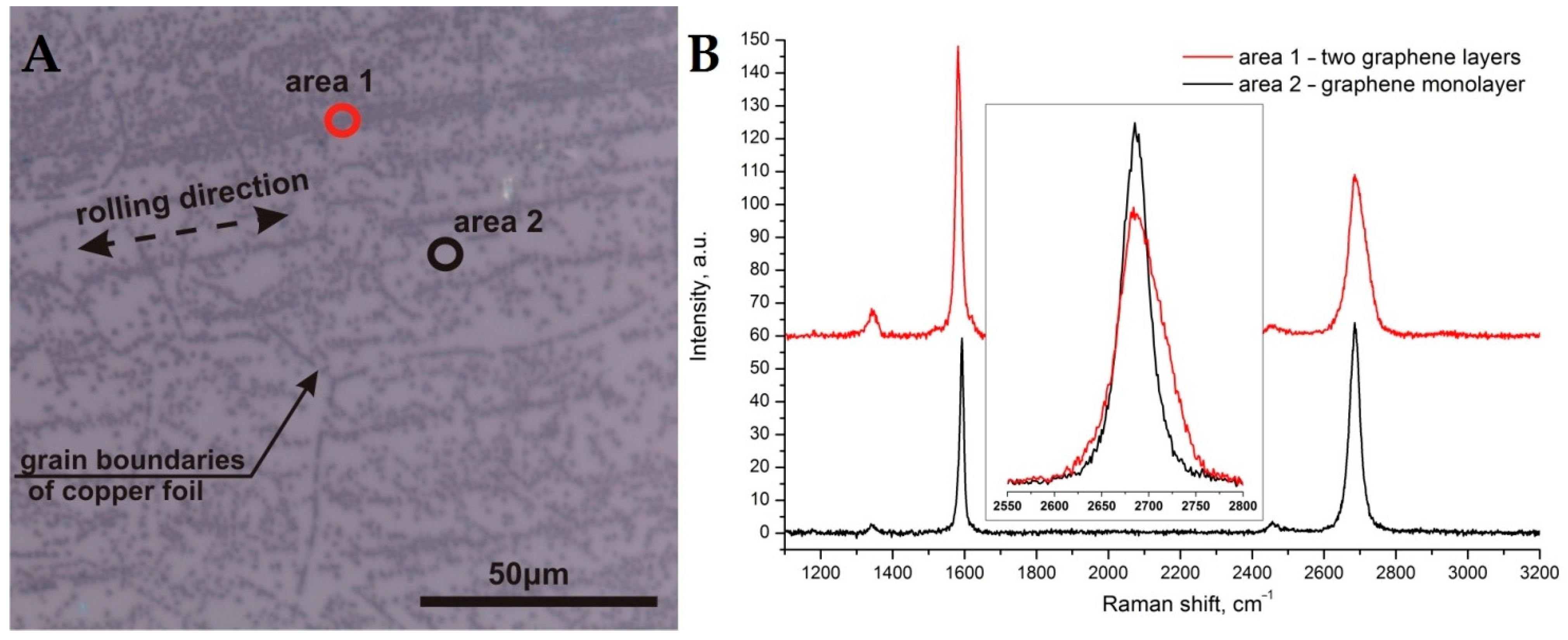
Abstract
:1. Introduction
2. Materials and Methods
2.1. Pretreatment of Copper Substrates
2.2. Copper Film Deposition
2.3. Graphene Growth Procedure
2.4. Transfer of the Grown Graphene
2.5. Sample Characterization
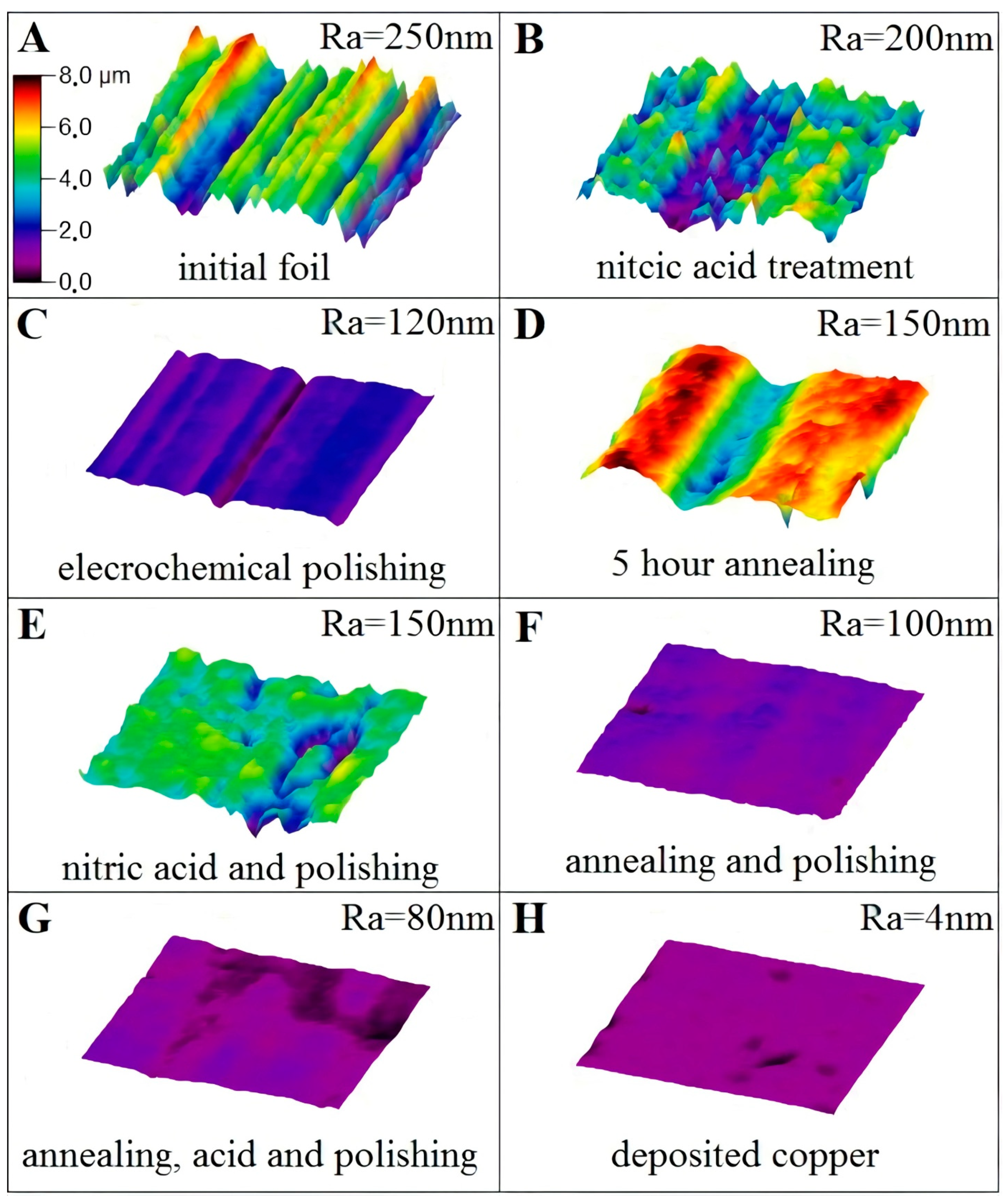
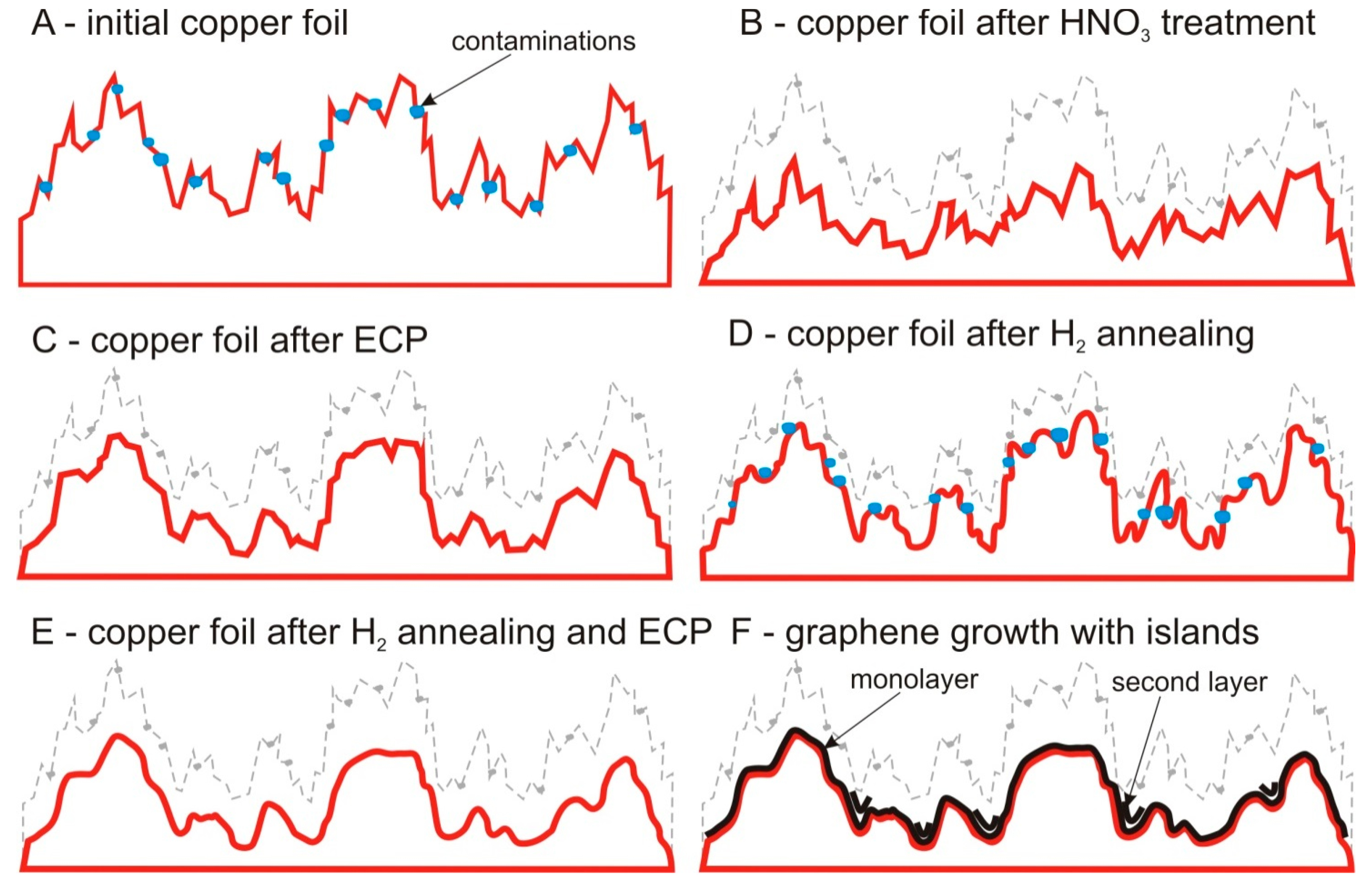
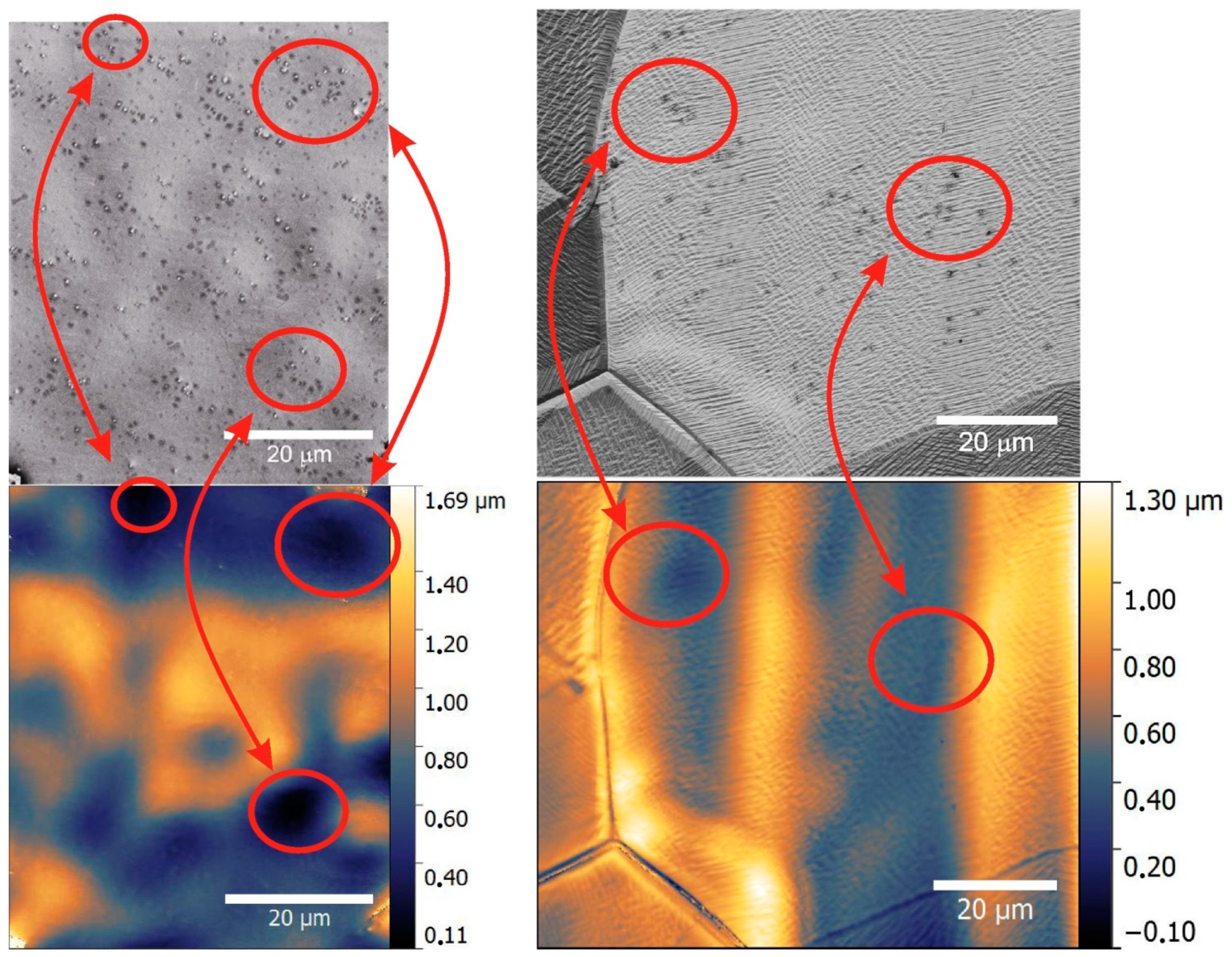
3. Results and Discussion
4. Conclusions
Supplementary Materials
Author Contributions
Funding
Data Availability Statement
Acknowledgments
Conflicts of Interest
References
- Li, X.; Cai, W.; An, J.; Kim, S.; Nah, J.; Yang, D.; Piner, R.; Velamakanni, A.; Jung, I.; Tutuc, E.; et al. Large-area synthesis of high-quality and uniform graphene films on copper foils. Science 2009, 324, 1312–1314. [Google Scholar] [CrossRef] [Green Version]
- McLellan, R.B. The solubility of carbon in solid gold, copper, and silver. Scr. Metall. 1969, 3, 389–391. [Google Scholar] [CrossRef]
- Luo, Z.; Lu, Y.; Singer, D.W.; Berck, M.E.; Somers, L.A.; Goldsmith, B.R.; Johnson, A.C. Effect of substrate roughness and feedstock concentration on growth of wafer-scale graphene at atmospheric pressure. Chem. Mater. 2011, 23, 1441–1447. [Google Scholar] [CrossRef]
- Yazyev, O.V.; Louie, S.G. Electronic transport in polycrystalline graphene. Nat. Mater. 2010, 9, 806–809. [Google Scholar] [CrossRef] [PubMed] [Green Version]
- Frank, O.; Vejpravova, J.; Holy, V.; Kavan, L.; Kalbac, M. Interaction between graphene and copper substrate: The role of lattice orientation. Carbon 2014, 68, 440–451. [Google Scholar] [CrossRef] [Green Version]
- He, R.; Zhao, L.; Petrone, N.; Kim, K.S.; Roth, M.; Hone, J.; Kim, P.; Pasupathy, A.; Pinczuk, A. Large physisorption strain in chemical vapor deposition of graphene on copper substrates. Nano Lett. 2012, 12, 2408–2413. [Google Scholar] [CrossRef] [Green Version]
- Vlassiouk, I.; Fulvio, P.; Meyer, H.; Lavrik, N.; Dai, S.; Datskos, P.; Smirnov, S. Large scale atmospheric pressure chemical vapor deposition of graphene. Carbon 2013, 54, 58–67. [Google Scholar] [CrossRef]
- Sarajlic, O.I.; Mani, R.G. Mesoscale scanning electron and tunneling microscopy study of the surface morphology of thermally annealed copper foils for graphene growth. Chem. Mater. 2013, 25, 1643–1648. [Google Scholar] [CrossRef]
- Chuang, M.C.; Woon, W.Y. Nucleation and growth dynamics of graphene on oxygen exposed copper substrate. Carbon 2016, 103, 384–390. [Google Scholar] [CrossRef]
- Xu, X.; Zhang, Z.; Dong, J.; Yi, D.; Niu, J.; Wu, M.; Lin, L.; Yin, R.; Li, M.; Zhou, J. Ultrafast epitaxial growth of metre-sized single-crystal graphene on industrial Cu foil. Sci. Bull. 2017, 62, 1074–1080. [Google Scholar] [CrossRef] [Green Version]
- Dhingra, S.; Hsu, J.F.; Vlassiouk, I.; D’Urso, B. Chemical vapor deposition of graphene on large-domain ultra-flat copper. Carbon 2014, 69, 188–193. [Google Scholar] [CrossRef]
- Murdock, A.T.; Van Engers, C.D.; Britton, J.; Babenko, V.; Meysami, S.S.; Bishop, H.; Crossley, A.; Koos, A.A.; Grobert, N. Targeted removal of copper foil surface impurities for improved synthesis of CVD graphene. Carbon 2017, 122, 207–216. [Google Scholar] [CrossRef]
- Kim, S.M.; Hsu, A.; Lee, Y.H.; Dresselhaus, M.; Palacios, T.; Kim, K.K.; Kong, J. The effect of copper pre-cleaning on graphene synthesis. Nanotechnology 2013, 24, 365602. [Google Scholar] [CrossRef]
- Mun, J.H.; Cho, B.J. Synthesis of monolayer graphene having a negligible amount of wrinkles by stress relaxation. Nano Lett. 2013, 13, 2496–2499. [Google Scholar] [CrossRef]
- Cho, S.Y.; Kim, H.M.; Lee, M.H.; Lee, D.J.; Kim, K.B. Single-step formation of a graphene–metal hybrid transparent and electrically conductive film. Nanotechnology 2012, 23, 115301. [Google Scholar] [CrossRef]
- Huet, B.; Raskin, J.P. Role of Cu foil in-situ annealing in controlling the size and thickness of CVD graphene domains. Carbon 2018, 129, 270–280. [Google Scholar] [CrossRef]
- Mohsin, A.; Liu, L.; Liu, P.; Deng, W.; Ivanov, I.N.; Li, G.; Dyck, O.E.; Duscher, G.; Dunlap, J.R.; Xiao, K.; et al. Synthesis of millimeter-size hexagon-shaped graphene single crystals on resolidified copper. ACS Nano 2013, 7, 8924–8931. [Google Scholar] [CrossRef]
- Nalini, S.; Thomas, S.; Jayaraj, M.K.; Sudarsanakumar, C.; Kumar, K.R. Chemical vapour deposited graphene: Substrate pre-treatment, growth and demonstration as a simple graphene-based SERS substrate. Bull. Mater. Sci. 2020, 43, 133. [Google Scholar] [CrossRef]
- Tay, R.Y.; Griep, M.H.; Mallick, G.; Tsang, S.H.; Singh, R.S.; Tumlin, T.; Teo, E.H.T.; Karna, S.P. Growth of large single-crystalline two-dimensional boron nitride hexagons on electropolished copper. Nano Lett. 2014, 14, 839–846. [Google Scholar] [CrossRef]
- Roy, S.S.; Jacobberger, R.M.; Wan, C.; Arnold, M.S. Controlling the density of pinhole defects in monolayer graphene synthesized via chemical vapor deposition on copper. Carbon 2016, 100, 1–6. [Google Scholar]
- Griep, M.H.; Sandoz-Rosado, E.; Tumlin, T.M.; Wetzel, E. Enhanced graphene mechanical properties through ultrasmooth copper growth substrates. Nano Lett. 2016, 16, 1657–1662. [Google Scholar] [CrossRef] [PubMed]
- Gnanaprakasa, T.J.; Gu, Y.X.; Eddy, S.K.; Han, Z.; Beck, W.J.; Muralidharan, K.; Raghavan, S. The role of copper pretreatment on the morphology of graphene grown by chemical vapor deposition. Microelectron Eng. 2015, 131, 1–7. [Google Scholar] [CrossRef]
- Zhang, B.; Lee, W.H.; Piner, R.; Kholmanov, I.; Wu, Y.; Li, H.; Ji, H.; Ruoff, R.S. Low-temperature Chemical Vapor Deposition Growth of Graphene from Toluene on Electropolished Copper Foils. ACS Nano 2012, 6, 2471–2476. [Google Scholar] [CrossRef] [PubMed]
- Li, X.; Colombo, L.; Ruoff, R.S. Synthesis of Graphene Films on Copper Foils by Chemical Vapor Deposition. Adv. Mater. 2016, 28, 6247–6252. [Google Scholar] [CrossRef]
- Barin, G.B.; Song, Y.; Gimenez, I.; Filho, L.G.S.; Barreto, L.S.; Kong, J. Optimized graphene transfer: Influence of polymethylmethacrylate (PMMA) layer concentration and baking time on graphene final performance. Carbon 2015, 84, 82–90. [Google Scholar] [CrossRef]
- Ferrari, A.; Basko, D. Raman spectroscopy as a versatile tool for studying the properties of graphene. Nat. Nanotechnol. 2013, 8, 235–246. [Google Scholar] [CrossRef] [Green Version]
- Braeuninger-Weimer, P.; Brennan, B.; Pollard, A.J.; Hofmann, S. Understanding and Controlling Cu-Catalyzed Graphene Nucleation: The Role of Impurities, Roughness, and Oxygen Scavenging. Chem. Mater. 2016, 28, 8905–8915. [Google Scholar] [CrossRef]
- Obelenis, F.; Champi, A. Determination of the Number of Graphene Layers on Different Substrates by Optical Microscopy Technique. Braz. J. Phys. 2014, 44, 682–686. [Google Scholar] [CrossRef]
- Bayle, M.; Reckinger, N.; Huntzinger, J.-R.; Felten, A.; Bakaraki, A.; Landois, P.; Colomer, J.-F.; Henrard, L.; Zahab, A.-A.; Sauvajol, J.-L.; et al. Dependence of the Raman spectrum characteristics on the number of layers and stacking orientation in few-layer graphene. Phys. Status Solidi B 2015, 252, 2375–2379. [Google Scholar] [CrossRef]


Publisher’s Note: MDPI stays neutral with regard to jurisdictional claims in published maps and institutional affiliations. |
© 2021 by the authors. Licensee MDPI, Basel, Switzerland. This article is an open access article distributed under the terms and conditions of the Creative Commons Attribution (CC BY) license (https://creativecommons.org/licenses/by/4.0/).
Share and Cite
Kondrashov, I.; Komlenok, M.; Pivovarov, P.; Savin, S.; Obraztsova, E.; Rybin, M. Preparation of Copper Surface for the Synthesis of Single-Layer Graphene. Nanomaterials 2021, 11, 1071. https://doi.org/10.3390/nano11051071
Kondrashov I, Komlenok M, Pivovarov P, Savin S, Obraztsova E, Rybin M. Preparation of Copper Surface for the Synthesis of Single-Layer Graphene. Nanomaterials. 2021; 11(5):1071. https://doi.org/10.3390/nano11051071
Chicago/Turabian StyleKondrashov, Ivan, Maxim Komlenok, Pavel Pivovarov, Sergey Savin, Elena Obraztsova, and Maxim Rybin. 2021. "Preparation of Copper Surface for the Synthesis of Single-Layer Graphene" Nanomaterials 11, no. 5: 1071. https://doi.org/10.3390/nano11051071