Article

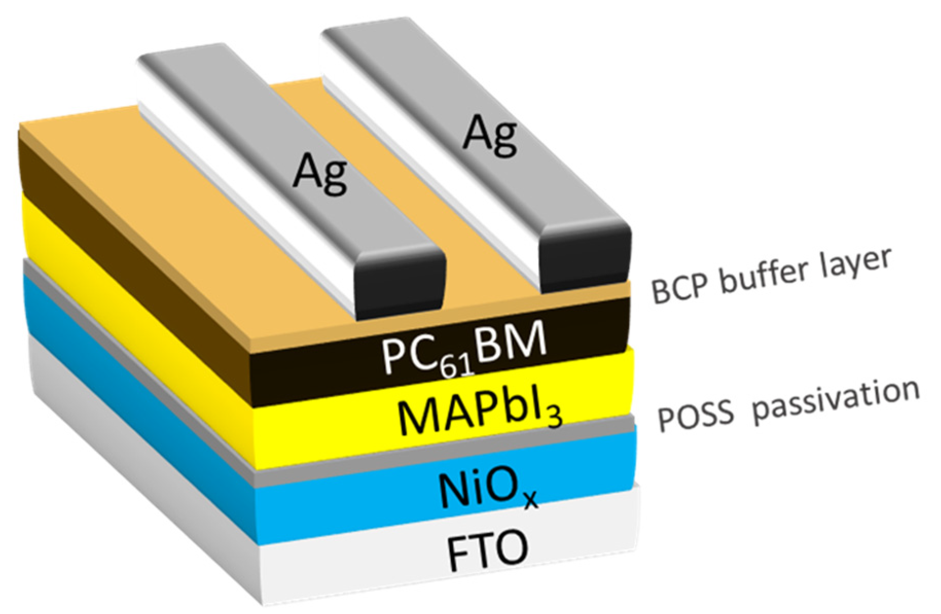
Fabrication and Characterization of an Efficient Inverted Perovskite Solar Cells with POSS Passivating Hole Transport Layer

1
Department of Chemical and Materials Engineering, National Yunlin University of Science and Technology, Yunlin 64002, Taiwan
2
Department of Chemical Engineering, National Chung Hsing University, Taichung 40227, Taiwan
3
School of Physics, Dublin City University, D09 W6Y4 Dublin, Ireland
4
Department of Electronic Engineering, National Yunlin University of Science and Technology, Yunlin 64002, Taiwan
*
Author to whom correspondence should be addressed.
Nanomaterials 2021, 11(4), 974; https://doi.org/10.3390/nano11040974
Submission received: 19 February 2021 / Revised: 29 March 2021 / Accepted: 7 April 2021 / Published: 10 April 2021

Abstract

:
Polyhedral oligomeric silsesquioxane (POSS), featuring a hollow-cage or semi-cage structure is a new type of organic–inorganic hybrid nanoparticles. POSS combines the advantages of inorganic components and organic components with a great potential for optoelectronic applications such as in emerging perovskite solar cells. When POSS is well dispersed in the polymer matrix, it can effectively improve the thermal, mechanical, magnetic, acoustic, and surface properties of the polymer. In this study, POSS was spin-coated as an ultra-thin passivation layer over the hole transporting layer of nickel-oxide (NOx) in the structure of a perovskite solar cell. The POSS incorporation led to a more hydrophobic and smoother surface for further perovskite deposition, resulting in the increase in the grain size of perovskite. An appropriate POSS passivation layer could effectively reduce the recombination of the electron and hole at grain boundaries and increase the short-circuit current from 18.0 to 20.5 mA·cm−2. Moreover, the open-circuit voltage of the cell could slightly increase over 1 V.

1. Introduction

In recent years, the perovskite solar cells (PSCs) have become considered among the most promising photovoltaic materials with rapidly increasing power conversion efficiency (PCE) from 3.8 to 25.5% in a very short period of time [1], owing to lightweight, low cost, simple fabrication, high optical absorption coefficient, and large charge carrier diffusion length. Compared to conventional PSCs, inverted cells with a device structure of transparent conductive oxide/hole transport layer (HTL)/perovskite/electron transport layer (ETL)/top metal electrode feature advantages of low-temperature processability and an immense potential for developing flexible optoelectronic devices [2,3]. Within the device structure of PSCs, both HTL and ETL serve as auxiliary layers to extract the charges from the perovskite layer and to deliver them to the respective electrodes while they also block the opposite charge transfer [4,5,6] and reduce the recombination near the interfaces. Poly(3,4-ethylenedioxythiophene):poly(styrene sulfonate) (PEDOT:PSS) is commonly used for the HTL within the structure of inverted PSCs. However, PEDOT:PSS possesses insufficient electron-blocking ability, high hygroscopicity, and poor chemical stability [7,8,9]. NiOX, being in favor of hole transport and blocking electrons efficiently, is one of the most potential alternatives to PEDOT:PESS. Moreover, NiOX leads to the higher open-circuit voltage (VOC) of PSCs because its work function exhibits a good alignment with valence band of CH3NH3PbI3 (MAPbI3) [10]. To reduce interfacial loss, a passivation layer has been inserted between the perovskite layer and the charge transport layer to decrease the interfacial defects and charge recombination [11,12,13]. Recently, several methods and materials, such as ultraviolet ozone [14], sodium dodecylbenzenesulfonate [15], and polystyrene [16], have been reported to passivate NOX and improve the crystal size of perovskite layer. Although they revealed enhanced efficiencies, few studies were reported about how to improve the NOX HTL for the fabrication of efficient PSCs. It remains a challenge to develop new passivation methods for the PSCs with NOX imported as HTL in their structure.
Polyhedral oligomeric silsesquioxane (POSS) possesses a hybrid structure of inorganic siloxane cage associated with organic groups. Combining hybrid and hollow characteristics, POSS exhibits special mechanical, electrical and optical properties as important building blocks for biomedical and optoelectronic materials [17,18]. The electron-withdrawing POSS cage potentially facilitates the dissociation of Li ions to increase the electrical conductivity of nanocomposite electrolytes [19]. POSS can block the undesirable anion exchange reactions to improve the water resistivity and surface coverage of CsPbX3 and be used as a hole blocking layer to balance the electron–hole injection of light-emitting devices [20,21]. Liu et al. used POSS with amino group to passivate perovskite layers through coordination and hydrogen bonding between amino groups and Pb ions. The passivation increased VOC and PCE owing to the decrease in the charge trap density and trap-state energy level [22]. The hydrophobic nature of POSS also improved the humidity tolerance of perovskite materials [23]. In this study, POSS was used in attempt to passivate the NOX HTL in a PSC structure through its hydrophobic nature and ability of trap suppression. Here, the PSCs have been fabricated with the inverted structure of fluorine-doped tin oxide (FTO)/NOX/POSS/MAPbI3/PC61BM/Bathocuproine (BCP)/Ag structure. The effect of POSS content on photovoltaic properties has been analyzed using different microscopy and spectroscopy techniques. Enhanced surface hydrophobicity and flatness were induced by the POSS passivation to significantly increase the grain size of perovskite. For an optimized concentration of 0.01-mg·mL−1 POSS, the short circuit current (JSC) increased from 18.0 to 20.5 mA·cm−2, an increase of 13.9%. This enhancement was mainly due to the decrease in grain boundaries and the resistance of the charge recombination.

2. Materials and Methods

2.1. Materials

FTO-coated glass substrates (7 Ω·sq−1) were purchased from Ruilong optoelectronics, Taiwan. Nickel(II) initrate hexahydrate (99.9985%), ethylene diamine (EDA, 99%), and ethylene glycol monomethyl ether (2-ME, 99%) were purchased from Alfa Aesar (Ward Hill, MA, USA). Acryloisobutyl POSS was received from Hybrid Plastics Inc. (Hatteriesburg, MS, USA). Methylammonium idodide (MAI), lead(II) iodide (PbI2), and bathocuproine (BCP, 99.5%) were purchased from Xi’an Polymer Light Technology (Xi’an, China). 6,6-Phenyl-C61-butyric acid methyl ester (PC61BM) were purchased from Solenne BV (Groningen, Netherlands). Anisole was purchased from Acros Organics (Geel, Belgium). Anhydrous solvents such as dimethyl sulfoxide (DMSO), dimethyl formamide (DMF), chlorobenzene (CB), and isopropanol (IPA) were purchased from Sigma Aldrich (Saint Louis, MO, USA) and used without further purification.

2.2. Synthesis of NOX Solution

The amount of 0.87 g nickel nitrate hexahydrate and 0.12 g of EDA were mixed into 5 mL of 2-ME. The solution was sealed with parafilm and stirred overnight at 550 rpm and 60 °C. The color of the solution gradually changed from dark green to dark blue, resulting in a 0.6 M NOX solution.

2.3. Device Fabrication

The fluorine doped tin oxide (FTO) glass substrates (2 × 1.5 cm2) were masked by polyimide tape as T-shape pattern. Then, the unmasked portion of the FTO was etched with zinc powder/HCl solution (6 M) and then cleaned with a detergent to remove the surface residue and zinc powder, following ultrasonically with ethanol, isopropanol, and deionized water for 15 min, respectively. The fabrication process of PSCs was illustrated in Figure S1. Typically, the NOX solution was spin-coated on the cleaned FTO glass substrates at 4000 rpm for 40 s and then heated at 100 °C for 10 min, followed by 300 °C for 1 h. 80 μL of POSS IPA solution in the concentration of 0, 0.005, 0.01, 0.015, and 0.05 mg·mL−1, was spin-coated on the as-prepared NiOX substrates at 6000 rpm for 20 s and then heated at 100 °C for 10 min, respectively. MAPbI3 was prepared by dissolving 0.2305-g MAI and 0.6684-g PbI2 in DMSO/DMF in the volumetric ratio of 1:4 and then stirring the solution for one day. Sixty microliters (60 μL) of the MAPbI3 solution was spin-coated on the POSS-passivated substrates at 4000 rpm for 25 s in a glove box. Nine seconds (9 s) after the start of the spinning, 500 μL of anisole was dropped upon the MAPbI3-coated substrates as an anti-solvent. The substrates were then heated at 100 °C for 12 min to complete the film formation. Ten microliters (10 μL) of PC61BM CB solution was spin-coated onto the perovskite layer at 3000 rpm for 20 s. Then, the samples were heated at 80 °C for 10 min. Eighty microliters (80 μL) of BCP IPA solution was spin-coated upon the PC61BM layer at 5000 rpm for 20 s. Finally, a silver layer with 100 nm thickness was formed on the surface of the devices through thermal deposition under a vacuum of 5 × 10⁻⁶ torr and a plating rate of 0.8–0.9 Å/s. The structure of the designed devices in this study is shown in Figure 1.

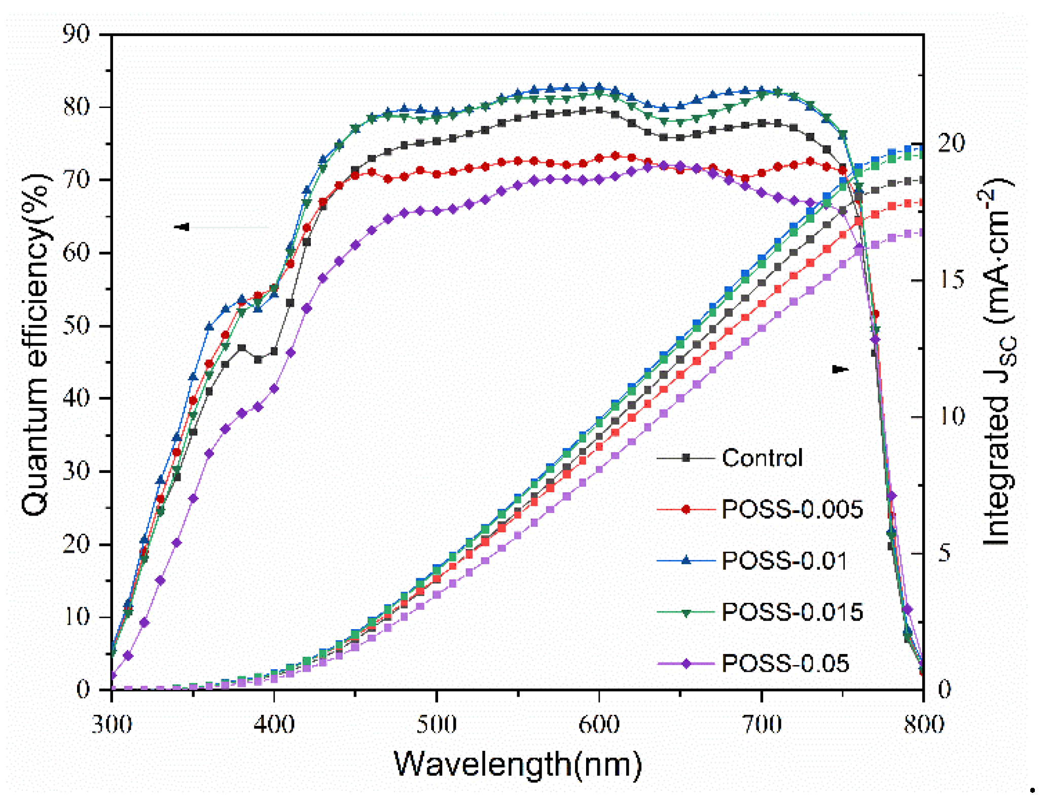
2.4. Measurements and Characterization

The crystalline phase of the perovskite crystals was characterized through X-ray diffraction (XRD) using an X-ray diffractometer (Miniflex II, Rigaku, Tokyo, Japan) and CuKα radiation (wavelength 0.15418 nm) with a fixed operating voltage of 30 kV and a fixed current of 15 mA. The morphology of the perovskite layers and devices were examined using a field-emission scanning electron microscope (AFE-SEM, Zeiss Auriga, Oberkochen, Germany). The absorption and photoluminescence (PL) emission spectra of the perovskite crystals were determined using a UV–Vis spectrometer (V770, Jasco, Tokyo, Japan) and a fluorescence spectrometer (LS-55, Perkin Elmer, Waltham, MA, USA), respectively. The contact angle of the POSS-passivated surface was determined using a contact angle analyzer (Phoenix 10, SEO, Suwon, Korea). The photocurrent density–voltage (J–V) characteristics were measured under irradiation of 100 mW·cm−2 using a solar simulator (MFS-PV, Hong-Ming Technology, Taiwan) equipped with a source meter (Keithley 2400, Keithley Instruments, Cleveland, OH, USA). Electrochemical impedance spectra (EIS) were measured over the frequency range of 50 mHz to 1 MHz with a potential perturbation of 10 mV using an electrochemical workstation (Zennium, Zahner, Kansas City, MO, USA). The incident photon-to-electron conversion efficiency (IPCE) spectra of cells were measured using an external quantum efficiency measurement system (QE-R, Enli Technology, Taiwan).

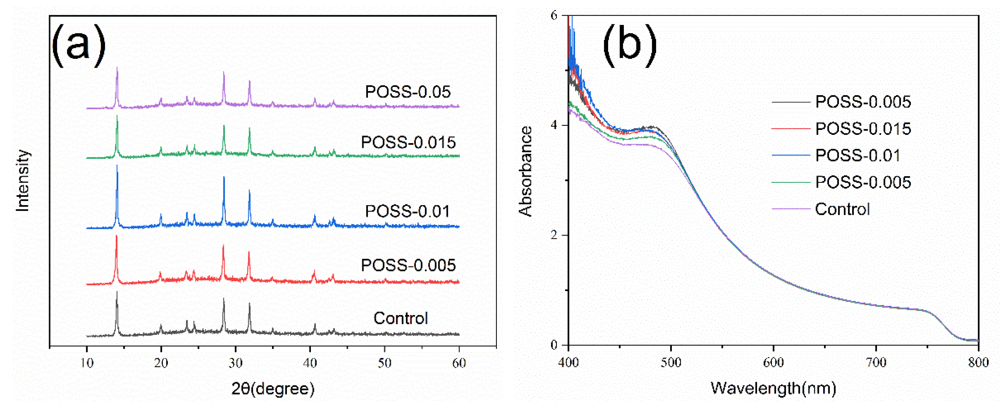
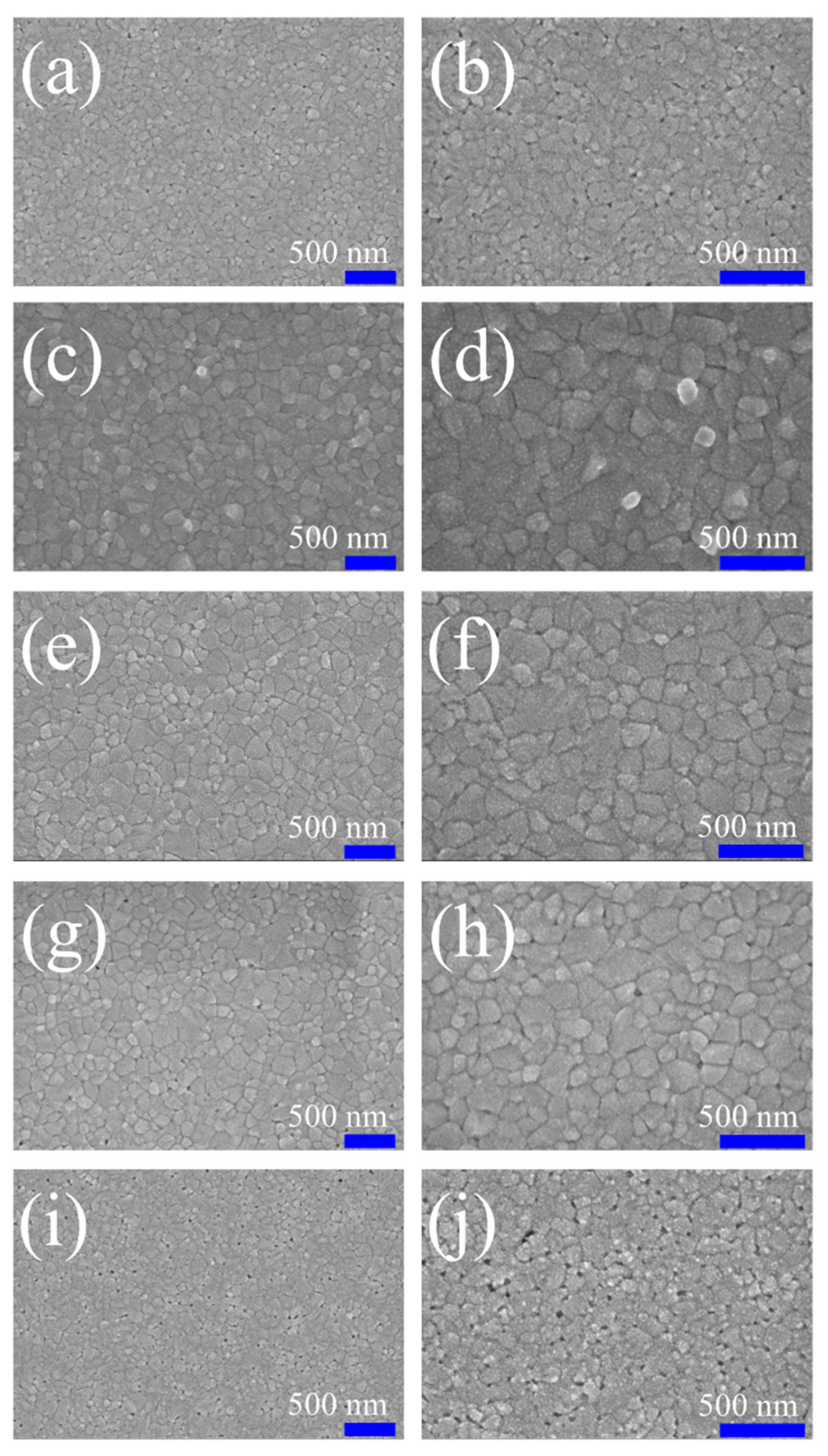
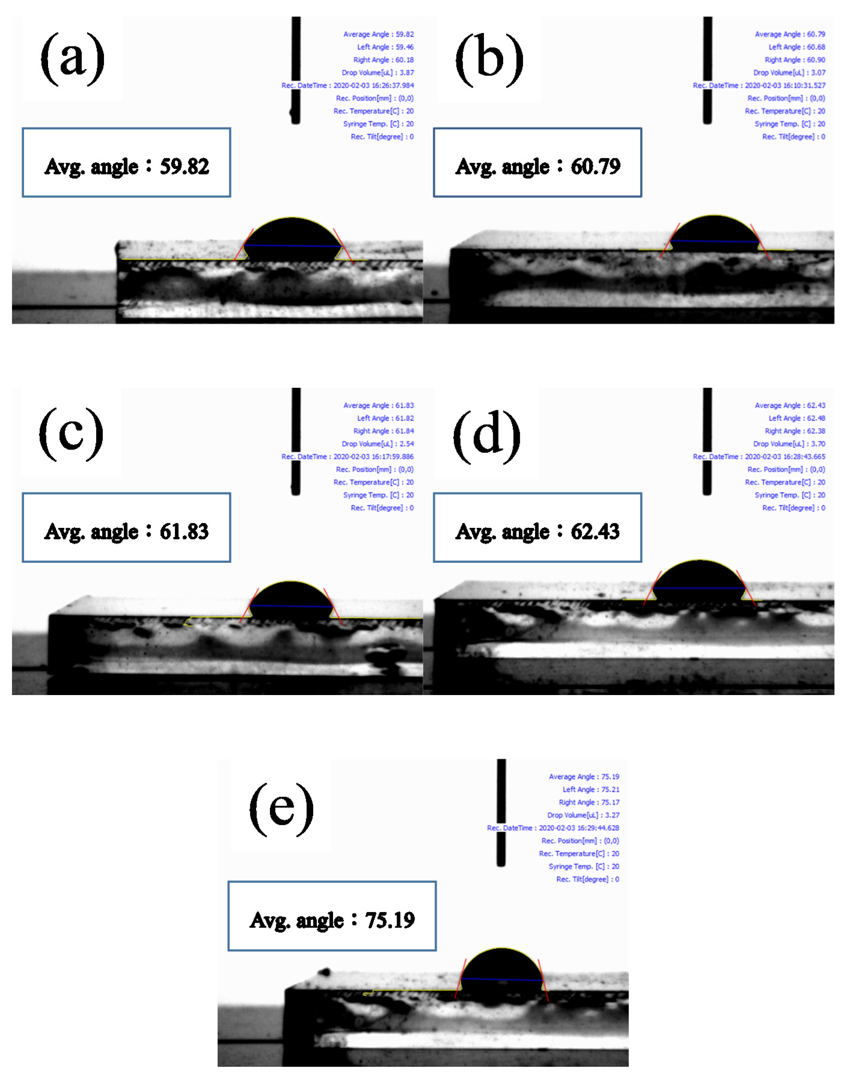
3. Results and Discussion

The XRD patterns of the perovskite layers with various POSS contents have been measured under dark standard conditions at room temperature and presented in Figure 2a. All samples exhibited three sharp reflection peaks at 14.1°, 28.4°, and 31.8° corresponding to crystal planes (110), (220), and (310) of tetragonal I4/mcm MAPbI3 perovskite structure, respectively [24]. These XRD results are in agreement with XRD patterns reported in the literature [25,26]. No peak has been recorded near 12.7° which is usually attributed to PbI2 formed in the perovskite layer [27]. This result implies that POSS incorporation neither hinders the formation of MAPbI3 crystal nor results in PbI2 separated out from MAPbI3 layer. In particular, the XRD peak related to plane (110) recorded for the sample POSS-0.01 shows the highest intensity compared to other samples, indicating that 0.01-mg·mL−1 POSS incorporation leads to the best crystallinity. Figure 2b shows the UV–Vis absorbance of the FTO/NiOX/POSS/MAPbI3 samples with various POSS incorporation. All of curves display the same cut-off edge at 779 nm but different absorption intensity in the range of 400~530 nm. Introduction of POSS over the NOX layer improves the photo-absorption of MAPbI3 and the strongest absorption rate is related to sample POSS-0.01.
Figure 3 presents the SEM surface morphology images of the MAPbI3 layers deposited over POSS layers fabricated with various POSS contents. The images were recorded at two kinds of magnification. Some pinholes can be observed on the surface of the pristine perovskite layer. When the ultra-thin POSS passivation layer is introduced, the number of pinholes is reduced and reaches the minimum level at concentration of 0.01-mg·mL−1 POSS, which means that the coverage of the perovskite layer is more complete at this optimum POSS concentration. When the POSS concentration increases over 0.01 mg·mL−1, the number of voids increases again. In addition to the pinholes, the POSS concentration also influences the grain size of MAPbI3. When the concentration of POSS increased from 0 to 0.01 mg·mL−1, the crystal growth of MAPbI3 progressively accelerated and the grain size of perovskite enlarged from 162.3 to 226.9 nm. However, grain size decreased to 167.5 nm when the POSS concentration increased to 0.05 mg·mL−1 (Figure S2). We inferred that too high and too low concentration of POSS may have a negative impact on the morphology and crystallinity of the perovskite layer. Figure 4 reveals the contact angle of water drops on the surface of FTO/NiOX/POSS with various POSS contents. It can be realized easily that the contact angle increases with POSS amount due to the hydrophobic nature of POSS. The hydrophobic property may reduce the damage of adsorbed water and hydroxyl groups on the surface of ETL to MAPbI3 crystal growth. Too many POSS may make the perovskite solution difficult to spread over the surface of substrates, resulting in pinholes and small grain size. The SEM analysis is in good correlation with the XRD and UV–Vis observations where all of them recommend that an optimum amount of POSS is a key to induce optimum crystal growth. A compact perovskite film with larger grains can be obtained at optimum POSS concentration with a full surface coverage (Figure 3e,f). Comparing with the pristine NiOX layer, an appropriate POSS deposition decreases the surface roughness (Figure S3). As a result, the increase in grain size of perovskite may be due to the fact that the POSS passivation makes the surface of the NiOX layer more hydrophobic and smoother. The photoluminescence spectra (PL) of the MAPbI3 grown over the substrate with various POSS amounts present a dominant peak around 753 nm under 500 nm excitation (Figure 5). Perovskites have a direct bandgap, thus this peak can be assigned to radiative recombination. The POSS-0.01 shows a slight blue shift to smaller wavelengths around 752 nm and also the PL intensity decreases. This represents the rapid transfer of the excited electrons into ETL which is due to improved grain size and improved film morphology with reduced pinholes.
Figure 6 displays the current–voltage characteristics of the PSCs with various POSS contents for passivation. The corresponding characteristic properties are summarized in Table 1. The PCEs and current densities of the PSCs increase with increasing POSS content, reaching a maximum at POSS-0.01, and decrease with further increasing POSS content (POSS-0.05). The order is reciprocal to that of the PL intensity but follows that of grain size. As the decrease in the PL intensity of MAPbI3 indicates the reduction in the rate of electron–hole recombination, the enhancement on PCEs and current density caused by the POSS passivation may result from the large grain size and few pinholes to reduce the charge recombination. Compared with pristine PSC (control), the POSS-0.01 increases the PCEs and the photocurrent density from 13.3 to 15.6% and from 18.0 to 20.5 mA·cm−2, an increase of 17.3 and 13.9%, respectively. Figure 7 presents the variations of device parameters (VOC, JSC, fill factor (FF), and PCE) of the control cell and the champion cell POSS-0.01. The individual data, average value, and standard deviation are shown in the figures. The higher average PCE and Jsc were obtained for POSS passivated cells. However, the average FF is lower for the POSS passivated cell which is probably due to increased series resistance of the passivated cells. However, the VOC of the POSS-0.01 is slightly higher than that of the control cell, responding the fact that lowering the charge recombination rate would lead to increasing VOC [28,29].
The Nyquist plots (Z′–Z′′) of the EIS of the PSCs with various POSS contents present two semicircles at the high and low frequency regions measured at V = VOC under dark conditions (Figure 8). We used an equivalent-circuit model, as inserted in Figure 8, to explain the EIS responses. R1 is the external series resistance including contacts resistance, CPE1 is related to the capacitive element at high-frequency response related to accumulation of surface charges at the interface of perovskite layer, R2 represents the charge transport resistance of the bulk perovskite film but contains information about the transport resistance of POSS passivation layer as well, and CPE2 represents the low-frequency capacitive related to the charge and defects accumulation in the film but can also be influenced from the ion in-diffusion recombination at the bulk of the film. R3 is the resistance related to the charge recombination at the bulk of the film due to presence of bulk defects and traps [30,31,32,33]. The fitting results are summarized in Table 1. With the increase in POSS content (POSS-0.005, POSS-0.01), the R2 and R3 increase, indicating that the charge recombination resistance increases but the charge transport resistance also increases. According to SEM morphology and absorption spectra analyses (Figure 2 and Figure 4), the decrease in charge recombination may be attributed to the increase in the grain size of MAPbI3. Larger grains and lower grain boundaries and thus reduce charge recombination at interfaces, consequently obtaining a higher JSC [34,35]. We infer that POSS passivation enhances the MAPbI3 crystal growth and thus blocks the ion-diffusion and defect/trap-related recombination in the perovskite layer, but also increases the resistance at the interface between the perovskite layer and the HTL. The increase in charge recombination resistance by POSS passivation is also observed by dark current analysis (Figure S4). The POSS-passivated cell displays a smaller leak current and dark current than the control cell, implying that the POSS passivation suppresses the charge recombination and induces a strong depleted electric field. Too many POSS contents may lead to the increase in pinhole, which increases the charge recombination rate but decreases the charge transport resistance. Figure 9 shows the IPCE spectra and integrated JSC of the control cell and the PSCs with various POSS contents. The values of the integrated JSC agreed well with those obtained from J–V measurement. The curves present a cutoff at ~790 nm, corresponding to a bandgap of 1.57 eV for a typical MAPbI3 solar cell [36]. POSS passivation influences mainly external quantum efficiency in the wavelength range of 380 to 760 nm. IPCE spectra of the PSCs support the J–V observation and the aforementioned argument. The POSS-0.01 displays the highest quantum efficiency and the highest JSC.

4. Conclusions

In summary, this is the first attempt to use POSS as a passivation layer between the hole transport layer (NiOX) and the perovskite layer (MAPbI3) of PSCs. POSS passivation can make the surface of the NiOX layer more hydrophobic and smoother surface, which leads to a significant increase in the MAPbI3 grain size and a slight increase in VOC. However, in addition to the increase in interface resistance, too much POSS makes the surface of NiOX become too hydrophobic to spread over the perovskite solution and thus results in pinholes and a small grain size. A 0.01-mg·mL−1 POSS passivation displays the best performance, which increases the JSC from 18.0 to 20.5 mA·cm−2 and an enhancement of 17.3% for PCE. The performance improvement arises mainly from the decrease in the rate of charge recombination.

Supplementary Materials

The following are available online at https://www.mdpi.com/article/10.3390/nano11040974/s1, Figure S1: Schematic representation of PSCs with POSS passivation; Figure S2: Average grain sizes of the MAPbI3 layers over various FTO/NiOX/POSS substrates, Figure S3: AFM topography images of the FTO/NiOX/POSS with various POSS contents; Figure S4: Dark current-voltage curves of the control cell and the champion cell.

Author Contributions

B.-T.L. conceptualized the work, designed the experiments, and wrote the manuscript. H.-R.L. conducted the fabrication and measurement of the cells. R.-H.L. and J.-C.C. helped the measurement. N.E.G. wrote the draft manuscript. All authors have read and agreed to the published version of the manuscript.

Funding

This research was funded by the Ministry of Science and Technology, Taiwan under grant number MOST 108-2221-E-224-026-MY3.

Data Availability Statement

The data presented in this study are available on request from the corresponding author.

Conflicts of Interest

The authors declare no conflict of interest.

References

  1. Best Research-Cell Efficiency Chart. Available online: https://www.nrel.gov/pv/cell-efficiency.html (accessed on 27 March 2021).
  2. You, J.; Hong, Z.; Yang, Y.; Chen, Q.; Cai, M.; Song, T.-B.; Chen, C.-C.; Lu, S.; Liu, Y.; Zhou, H.; et al. Low-temperature solution-processed perovskite solar cells with high efficiency and flexibility. ACS Nano 2014, 8, 1674–1680. [Google Scholar] [CrossRef]
  3. Docampo, P.; Ball, J.M.; Darwich, M.; Eperon, G.E.; Snaith, H.J. Efficient organometal trihalide perovskite planar-heterojunction solar cells on flexible polymer substrates. Nat. Commun. 2013, 4, 2761. [Google Scholar] [CrossRef] [Green Version]
  4. Jiang, Q.; Zhang, L.; Wang, H.; Yang, X.; Meng, J.; Liu, H.; Yin, Z.; Wu, J.; Zhang, X.; You, J. Enhanced electron extraction using SnO2 for high-efficiency planar-structure HC(NH2)2PbI3-based perovskite solar cells. Nat. Energy 2016, 2, 16177. [Google Scholar] [CrossRef]
  5. Green, M.A.; Ho-Baillie, A.; Snaith, H.J. The emergence of perovskite solar cells. Nat. Photon. 2014, 8, 506. [Google Scholar] [CrossRef]
  6. Edri, E.; Kirmayer, S.; Mukhopadhyay, S.; Gartsman, K.; Hodes, G.; Cahen, D. Elucidating the charge carrier separation and working mechanism of CH3NH3PbI3−xClx perovskite solar cells. Nat. Commun. 2014, 5, 3461. [Google Scholar] [CrossRef] [PubMed]
  7. Li, H.; Fu, K.; Boix, P.P.; Wong, L.H.; Hagfeldt, A.; Grätzel, M.; Mhaisalkar, S.G.; Grimsdale, A.C. Hole-transporting small molecules based on thiophene cores for high efficiency perovskite solar cells. ChemSusChem 2014, 7, 3420–3425. [Google Scholar] [CrossRef]
  8. Labban, A.E.; Chen, H.; Kirkus, M.; Barbe, J.; Del Gobbo, S.; Neophytou, M.; McCulloch, I.; Eid, J. Improved efficiency in inverted perovskite solar cells employing a novel diarylamino-substituted molecule as PEDOT:PSS replacement. Adv. Energy Mater. 2016, 6, 1502101. [Google Scholar] [CrossRef] [Green Version]
  9. Cheng, C.-J.; Balamurugan, R.; Liu, B.-T. Enhanced efficiencies of perovskite solar cells by incorporating silver nanowires into the hole transport layer. Micromachines 2019, 10, 682. [Google Scholar] [CrossRef] [PubMed] [Green Version]
  10. Jeng, J.-Y.; Chen, K.-C.; Chiang, T.-Y.; Lin, P.-Y.; Tsai, T.-D.; Chang, Y.-C.; Guo, T.-F.; Chen, P.; Wen, T.-C.; Hsu, Y.-J. Nickel oxide electrode interlayer in CH3NH3PbI3 perovskite/PCBM planar-heterojunction hybrid solar cells. Adv. Mater. 2014, 26, 4107–4113. [Google Scholar] [CrossRef]
  11. Kim, J.; Ho-Baillie, A.; Huang, S. Review of novel passivation techniques for efficient and stable perovskite solar cells. Solar RRL 2019, 3, 1800302. [Google Scholar] [CrossRef]
  12. Peng, J.; Wu, Y.; Ye, W.; Jacobs, D.A.; Shen, H.; Fu, X.; Wan, Y.; Wu, N.; Barugkin, C.; Nguyen, H.T. Interface passivation using ultrathin polymer–fullerene films for high-efficiency perovskite solar cells with negligible hysteresis. Energy Environ. Sci. 2017, 10, 1792–1800. [Google Scholar] [CrossRef] [Green Version]
  13. Liu, B.-T.; Guo, B.-W.; Balamurugan, R. Effect of polyethylene glycol incorporation in electron transport layer on photovoltaic properties of perovskite solar cells. Nanomaterials 2020, 10, 1753. [Google Scholar] [CrossRef]
  14. Wang, T.; Ding, D.; Zheng, H.; Wang, X.; Wang, J.; Liu, H.; Shen, W. Efficient inverted planar perovskite solar cells using ultraviolet/ozone-treated NiOx as the hole transport layer. Solar RRL 2019, 3, 1900045. [Google Scholar] [CrossRef]
  15. Wang, T.; Xie, M.; Abbasi, S.; Cheng, Z.; Liu, H.; Shen, W. High efficiency perovskite solar cells with tailorable surface wettability by surfactant. J. Power Sources 2020, 448, 227584. [Google Scholar] [CrossRef]
  16. Wang, T.; Cheng, Z.; Zhou, Y.; Liu, H.; Shen, W. Highly efficient and stable perovskite solar cells via bilateral passivation layers. J. Mater. Chem. A 2019, 7, 21730–21739. [Google Scholar] [CrossRef]
  17. Shi, H.; Yang, J.; You, M.; Li, Z.; He, C. Polyhedral oligomeric silsesquioxanes (POSS)-based hybrid soft gels: Molecular design, material advantages, adn emerging applications. ACS Mater. Lett. 2020, 2, 296–316. [Google Scholar] [CrossRef]
  18. Li, Z.; Kong, J.; Wang, F.; He, C. Polyhedral oligomeric silsesquioxanes (POSSs): An important building block for organic optoelectronic materials. J. Mater. Chem. C 2017, 5, 5283–5298. [Google Scholar] [CrossRef]
  19. Chinnam, P.R.; Wunder, S.L. Polyoctahedral silsesquioxane-nanoparticle electrolytes for lithium batteries: POSS-lithium salts and POSS-PEGs. Chem. Mater. 2011, 23, 5111–5121. [Google Scholar] [CrossRef]
  20. Huang, H.; Chen, B.; Wang, Z.; Hung, T.F.; Susha, A.S.; Zhong, H.; Rogach, A.L. Water resistant CsPbX3 nanocrystals coated with polyhedral oligomeric silsesquioxane and their use as solid state luminophores in all-perovskite white light-imitting devices. Chem. Sci. 2016, 7, 5699–5703. [Google Scholar] [CrossRef] [Green Version]
  21. Huang, H.; Lin, H.; Kershaw, S.V.; Susha, A.S.; Choy, W.C.; Rogach, A.L. Polyhedral oligomeric silsesquioxane enhances the brightness of perovskite nanocrystal-based green light-emitting devices. J. Phys. Chem. Lett. 2016, 7, 4398–4404. [Google Scholar] [CrossRef]
  22. Liu, N.; Du, Q.; Yin, G.; Liu, P.; Li, L.; Xie, H.; Zhu, C.; Li, Y.; Zhou, H.; Zhang, W.-B. Extremely low trap-state energy level perovskite solar cells passivated using NH2-POSS with improved efficiency and stability. J. Mater. Chem. A 2018, 6, 6806–6814. [Google Scholar] [CrossRef]
  23. Li, L.; Jin, X.; Liu, N.; Chen, Q.; Zhang, W.B.; Zhou, H. Efficient moisture-resistant perovskite solar cell with nanostructure featuring 3D amine motif. Solar RRL 2018, 2, 1800069. [Google Scholar] [CrossRef]
  24. Pellegrino, G.; Colella, S.; Deretzis, I.; Condorelli, G.G.; Smecca, E.; Gigli, G.; La Magna, A.; Alberti, A. Texture of MAPbI3 layers assisted by chloride on flat TiO2 substrates. J. Phys. Chem. C 2015, 119, 19808–19816. [Google Scholar] [CrossRef]
  25. Zhang, Q.; Yu, H.; Zhao, F.; Pei, L.; Li, J.; Wang, K.; Hu, B. Substrate-dependent spin–orbit coupling in hybrid perovskite thin films. Adv. Funct. Mater. 2019, 29, 1904046. [Google Scholar] [CrossRef]
  26. Li, D.; Bretschneider, S.A.; Bergmann, V.W.; Hermes, I.M.; Mars, J.; Klasen, A.; Lu, H.; Tremel, W.; Mezger, M.; Butt, H.-J.r. Humidity-induced grain boundaries in MAPbI3 perovskite films. J. Phys. Chem. C 2016, 120, 6363–6368. [Google Scholar] [CrossRef]
  27. Shirayama, M.; Kato, M.; Miyadera, T.; Sugita, T.; Fujiseki, T.; Hara, S.; Kadowaki, H.; Murata, D.; Chikamatsu, M.; Fujiwara, H. Degradation mechanism of CH3NH3PbI3 perovskite materials upon exposure to humid air. J. Appl. Phys. 2016, 119, 115501. [Google Scholar] [CrossRef] [Green Version]
  28. Wang, W.; Zhang, Z.; Cai, Y.; Chen, J.; Wang, J.; Huang, R.; Lu, X.; Gao, X.; Shui, L.; Wu, S.; et al. Enhanced performance of CH3NH3PbI3−xClx perovskite solar cells by CH3NH3I modification of TiO2-perovskite layer interface. Nanoscale Res. Lett. 2016, 11, 316. [Google Scholar] [CrossRef] [Green Version]
  29. Li, P.-S.; Balamurugan, R.; Liu, B.-T.; Lee, R.-H.; Chou, H.-T. MAPbI3 incorporated with carboxyl group chelated titania for planar perovskite solar cells in low-temperature process. Nanomaterials 2019, 9, 908. [Google Scholar] [CrossRef] [PubMed] [Green Version]
  30. Yang, D.; Zhou, X.; Yang, R.; Yang, Z.; Yu, W.; Wang, X.; Li, C.; Liu, S.F.; Chang, R.P. Surface optimization to eliminate hysteresis for record efficiency planar perovskite solar cells. Energy Environ. Sci. 2016, 9, 3071–3078. [Google Scholar] [CrossRef]
  31. Zhu, Z.; Xue, Q.; He, H.; Jiang, K.; Hu, Z.; Bai, Y.; Zhang, T.; Xiao, S.; Gundogdu, K.; Gautam, B.R. A PCBM electron transport layer containing small amounts of dual polymer additives that enables enhanced perovskite solar cell performance. Adv. Sci. 2016, 3, 1500353. [Google Scholar] [CrossRef]
  32. Song, J.; Yang, Y.; Zhao, Y.; Che, M.; Zhu, L.; Gu, X.; Qiang, Y. Morphology modification of perovskite film by a simple post-treatment process in perovskite solar cell. Mater. Sci. Eng. B 2017, 217, 18–25. [Google Scholar] [CrossRef]
  33. Park, M.; Kim, J.-Y.; Son, H.J.; Lee, C.-H.; Jang, S.S.; Ko, M.J. Low-temperature solution-processed Li-doped SnO2 as an effective electron transporting layer for high-performance flexible and wearable perovskite solar cells. Nano Energy 2016, 26, 208–215. [Google Scholar] [CrossRef]
  34. Kim, H.D.; Ohkita, H.; Benten, H.; Ito, S. Photovoltaic performance of perovskite solar cells with different grain sizes. Adv. Mater. 2016, 28, 917–922. [Google Scholar] [CrossRef] [PubMed] [Green Version]
  35. Ren, X.; Yang, Z.; Yang, D.; Zhang, X.; Cui, D.; Liu, Y.; Wei, Q.; Fan, H.; Liu, S. Modulating crystal grain size and optoelectronic properties of perovskite films for solar cells by reaction temperature. Nanoscale 2016, 8, 3816–3822. [Google Scholar] [CrossRef] [PubMed]
  36. Atourki, L.; Vega, E.; Mari, B.; Mollar, M.; Ahsaine, H.A.; Bouabid, K.; Ihlal, A. Role the chemical substitution on the structural and luminescence properties of the mixed halide perovskite thin MAPbI3-xBrx (0 ≤ x ≤ 1) films. Appl. Surf. Sci. 2016, 371, 112–117. [Google Scholar]
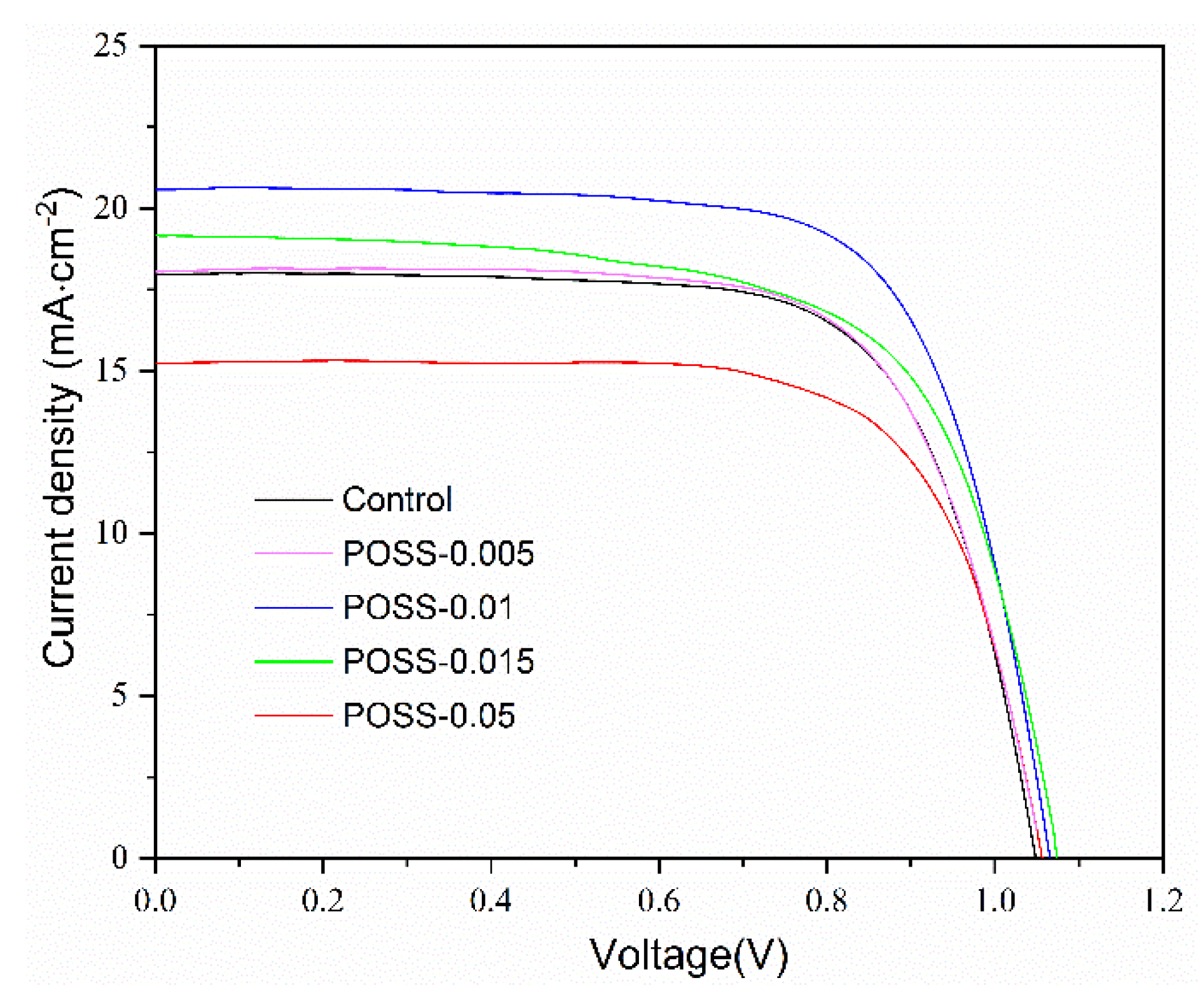
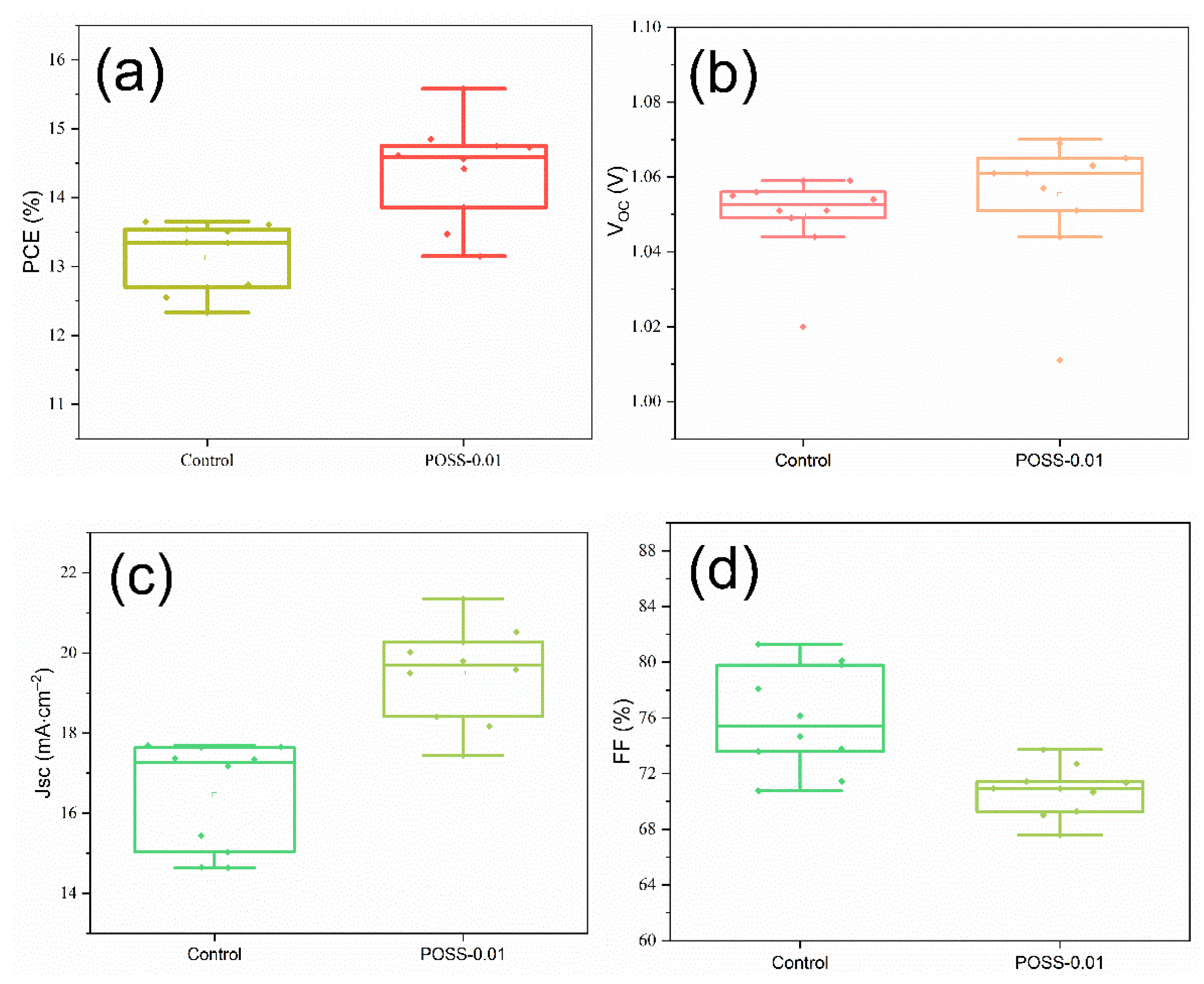
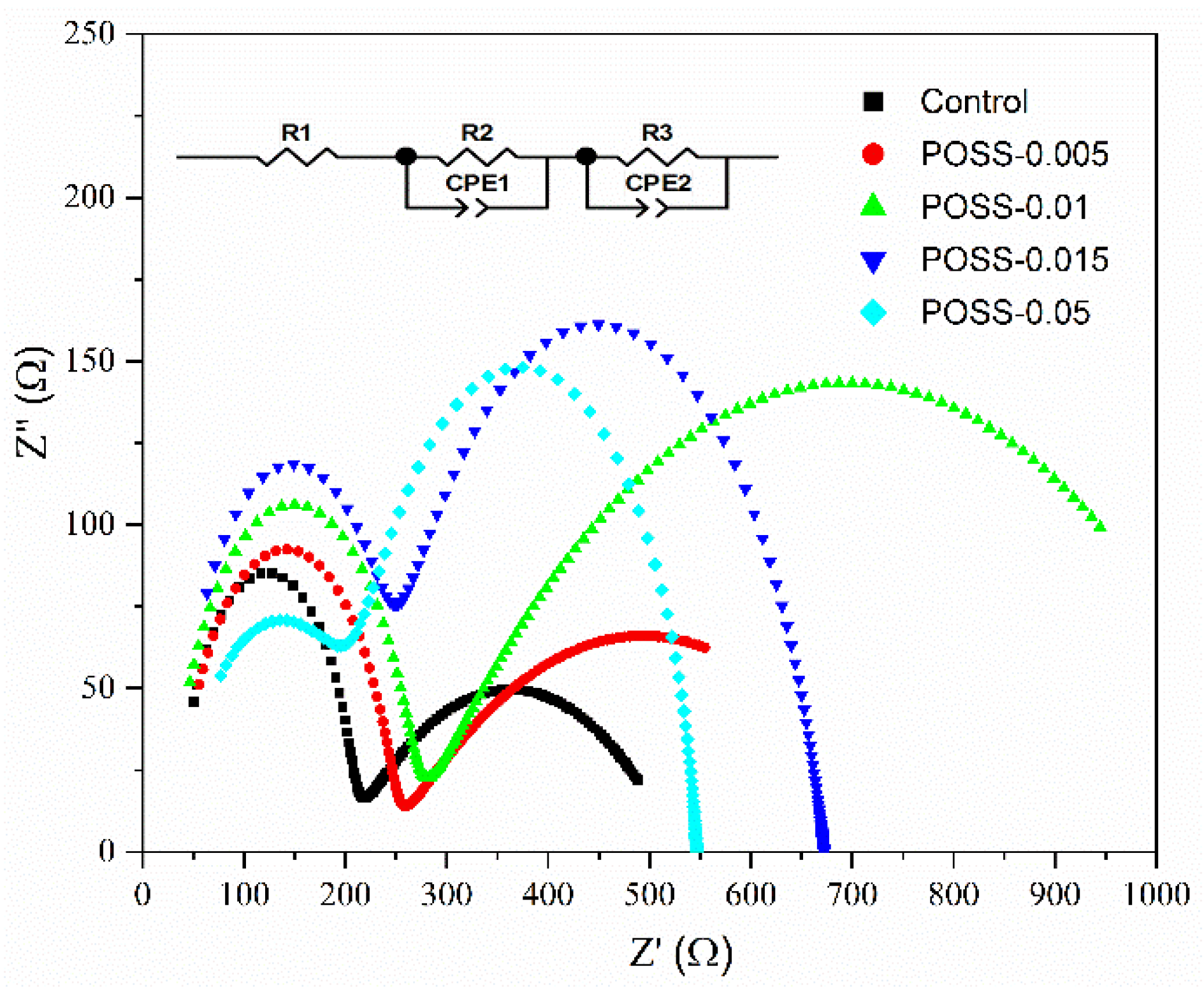
Figure 1. The schematic representation of structure of designed perovskite solar cells (PSCs).
Nanomaterials 11 00974 g001
Figure 2. (a) XRD patterns and (b) UV–Vis absorption spectra of the MAPbI3 layers over the fluorine-doped tin oxide (FTO)/NiOX/POSS with various POSS contents.
Nanomaterials 11 00974 g002
Figure 3. SEM images of the MAPbI3 layers over the FTO/NiOX/POSS with various POSS contents: (a,b) control; (c,d) POSS-0.005; (e,f) POSS-0.01; (g,h) POSS-0.015; and (i,j) POSS-0.05. The magnification in the left images and the right images are x30k and x50k, respectively.
Nanomaterials 11 00974 g003
Figure 4. Drop images of the MAPbI3 layers over the FTO/NiOX/POSS with various POSS contents and their corresponding contact angle: (a) control; (b) POSS-0.005; (c) POSS-0.01; (d) POSS-0.015; and (e) POSS-0.05.
Nanomaterials 11 00974 g004
Figure 5. Photoluminescence spectra (PL) spectra of the FTO/NiOX/POSS/MAPbI3 with various POSS contents.
Nanomaterials 11 00974 g005
Figure 6. Current–voltage characteristics of the control cell and the PSC fabricated with various POSS contents.
Nanomaterials 11 00974 g006
Figure 7. Distribution of device metrics for 10 cells fabricated without and with POSS passivation layer: (a) PCE; (b) VOC; (c) JSC; and (d) FF.
Nanomaterials 11 00974 g007
Figure 8. Nyquist plots of the electrochemical impedance spectra (EIS) of the control cell and the PSC fabricated with various POSS contents.
Nanomaterials 11 00974 g008
Figure 9. IPCE spectra and integrated JSC of the control cell and the PSCs with various POSS contents.
Nanomaterials 11 00974 g009
Table 1. The photovoltaic characteristics of the control cell and the PSC fabricated with various POSS contents.
SamplesPOSS Concentration
mg·mL−1
Voc, VJsc, mA·cm−2FF, %PCE (Average PCE), %R2, ΩR3, Ω
Control01.0518.070.1813.3 (12.55 ± 0.49)163.9328.9
POSS-0.0050.0051.0518.473.7814.1 (12.64 ± 1.23)209.2506.4
POSS-0.010.011.0720.571.3315.6 (14.75 ± 0.71)234.3869.9
POSS-0.0150.0151.0719.266.1613.7 (12.85 ± 0.35)193.7440.3
POSS-0.050.051.0615.271.6011.5 (10.91 ± 0.62)179.3332.7
Publisher’s Note: MDPI stays neutral with regard to jurisdictional claims in published maps and institutional affiliations.

