Review

Recent Progress on Vanadium Dioxide Nanostructures and Devices: Fabrication, Properties, Applications and Perspectives

1
State Key Laboratory of Optoelectronic Materials and Technologies, School of Physics, Sun Yat-sen University, Guangzhou 510275, China
2
Centre for Physical Mechanics and Biophysics, School of Physics, Sun Yat-sen University, Guangzhou 510275, China
3
School of Materials, Sun Yat-sen University, Guangzhou 510275, China
*
Authors to whom correspondence should be addressed.
Nanomaterials 2021, 11(2), 338; https://doi.org/10.3390/nano11020338
Submission received: 23 December 2020 / Revised: 19 January 2021 / Accepted: 20 January 2021 / Published: 28 January 2021

Abstract

:
Vanadium dioxide (VO2) is a typical metal-insulator transition (MIT) material, which changes from room-temperature monoclinic insulating phase to high-temperature rutile metallic phase. The phase transition of VO2 is accompanied by sudden changes in conductance and optical transmittance. Due to the excellent phase transition characteristics of VO2, it has been widely studied in the applications of electric and optical devices, smart windows, sensors, actuators, etc. In this review, we provide a summary about several phases of VO2 and their corresponding structural features, the typical fabrication methods of VO2 nanostructures (e.g., thin film and low-dimensional structures (LDSs)) and the properties and related applications of VO2. In addition, the challenges and opportunities for VO2 in future studies and applications are also discussed.

1. Introduction

A phase transition is a sudden change of one phase to another under an external stimuli, e.g., a thermal field, strain energy, surface energy, an external force, a magnetic field, etc., accompanied by the significant change in physical properties. Metal–insulator transition (MIT) is one of the typical phase transition types in oxides, and has been a research hotspot in recent decades. Among inorganic materials with MIT, vanadium dioxide (VO2) is widely focused on because of the near-room-temperature phase transition temperature (Tc ≈ 340 K) and the reversible, huge changes in conductance and transmittance during MIT [1,2]. This reversible phase transition is a first-order phase transition, which is accompanied by a crystal structure change from a low-temperature monoclinic phase to a high-temperature rutile phase. Besides, the strongly correlated electron effect introduced by the special d electron orbit structure of VO2 leads to abundant interesting physical and chemical properties. Based on these excellent performances, VO2 can be widely used in many fields and has been becoming one of the hottest metal oxide materials in recent years [3,4,5,6,7,8,9]. Moreover, the rapid development in VO2 preparation and performance modulation technologies has greatly promoted the application of VO2 in many aspects; e.g., VO2 can be used as a channel layer of field-effect transistor (FET) due to its electric-field-adjustable MIT behavior. The distinctive hysteresis loop during the MIT process under an electric filed or temperature change leads to applications in memory devices; the great difference of transmittance between the insulating and metallic phases makes it a candidate material for smart windows; the strain and gas-environment-dependent MIT behavior holds promise for developing novel strain and gas sensors, etc., [6,10,11,12,13].
With the development of material fabrication technology, various VO2 nanostructures, e.g., thin films and low-dimensional structures (LDSs), have been successfully fabricated and have been widely investigated. Thin films and LDSs are suitable for micromachining processes, which promotes the development of both macro- and micro-scale devices. As we know, the MIT temperature and behavior of VO2 are extremely sensitive to external stimuli, including doping, strain, surface/interface effects, electrochemical gating, electric field, light, electron beam, etc. [6,14,15,16,17,18,19,20]. Besides, the morphology also has a great influence on the properties of VO2 material. VO2 LDSs—nanowires (NWs), nanodots (NDs), nanoparticles (NPs), nanorods (NRs), nanobelts (NBs), nanosheets (NSs), etc.—exhibit unique electrical, mechanical and optical properties different from their bulk counterparts due to the size and surface/interface effects. Recently, VO2 thin films and LDSs have been successfully fabricated via advanced growth techniques and have attracted much attention.
On the basis of a survey of excellent experimental works on VO2, we aim to provide a wide range of insights into the recent studies in this field. In Section 2, the multiple phases of VO2 are primarily introduced. We emphasize the performances of different phases and the transform paths among them. In Section 3, several commonly used methods—e.g., the hydrothermal method, chemical vapor deposition (CVD), pulsed laser deposition (PLD), sol–gel, magnetron sputtering, electrospinning and molecular beam epitaxy (MBE) are introduced. These methods have unique characteristics in the fabrication of VO2 nanostructures and can be employed to realize abound VO2 nanostructures, including NDs, NWs, NRs, NSs, NPs, nanoplates, nanorings, thin films, etc. In Section 4, the properties and the applications of VO2 nanostructures are summarized and discussed. Finally, the challenges and opportunities of VO2 in future studies and applications are also discussed.

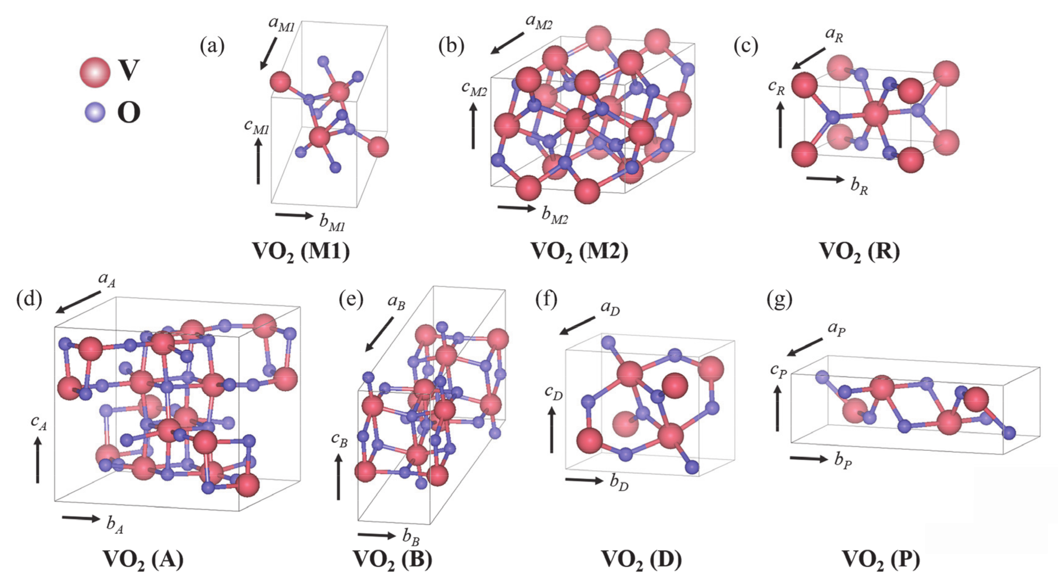
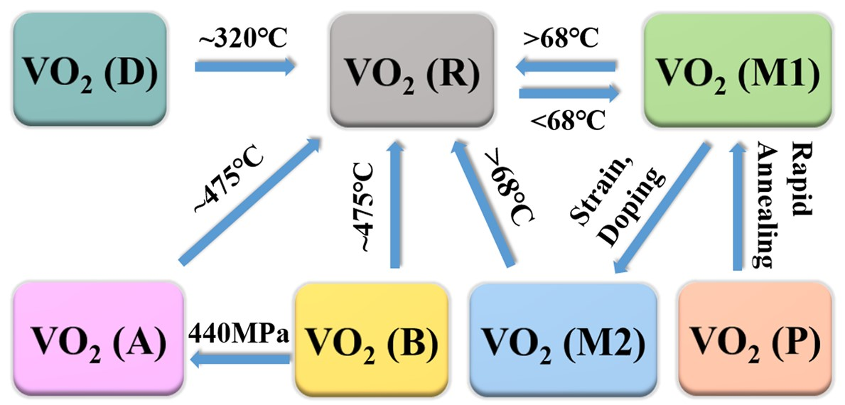
2. Overview of VO2 Polymorphs

At present, several phases of VO2 have been reported, including VO2 (M) (P 21/c), VO2 (R) (P 42/mnm), VO2 (A) (P 42/nmc), VO2 (B) (C 2/m), VO2 (C) (I 4/mmm), VO2 (D) (P 2/c) and VO2 (P) (Pbnm), as shown in Table 1 [21,22,23,24,25,26,27,28,29,30]. Additionally, the corresponding crystal structures are displayed in Figure 1. Under certain conditions, these phases can be transformed into each other (Figure 2) [25,26,31,32,33].
Among these phases, VO2 (M), VO2 (R), VO2 (A) and VO2 (B) have the most common crystal structures. The basic structural unit is the VO6 octahedron—i.e., a vanadium atom is in the center of the octahedron and is surrounded by six oxygen atoms. Octahedrons are arranged by common edges or vertices, and a long-range ordered structure is formed in three-dimensional space. For VO2 crystals with different crystal structures, the shape of the VO6 octahedron and the connection modes between octahedrons are different, which leads to the differences of atomic coordinates and spatial symmetry groups. VO2 (M) is an insulating monoclinic phase containing VO2 (M1) and VO2 (M2) phases. Generally, the MIT of VO2 is the transition of VO2 (M1) into VO2 (R) after exceeding the MIT temperature. The low-temperature monoclinic phase is an insulating phase (M or M1 phase, space group P 21/c, aM = 5.715 Å, bM = 4.554 Å, cM = 5.385 Å, β = 122.6°) and the high-temperature rutile phase is a metal phase (R phase, space group P 42/mnm, aR = bR = 4.554 Å, cR = 2.85 Å, β = 90°) [21,22]. In the low-temperature monoclinic phase, V atoms form zigzag structure along the direction of c axis. In the high-temperature rutile phase, V atoms form a straight line along the direction of c axis with the period of 1/2 × cM. During the phase transition from insulating phase to metal phase, the octahedral structure composed of V–O changes from the partial octahedron at a low temperature to the normal octahedron at a high temperature, and the V–O bond angle changes from 90° to 78–99° (Figure 1c). In addition, compared with the high-temperature tetragonal phase, the lattice constants a and b of M phase are increased by ~0.6% and ~0.4%, respectively. Meanwhile, c is decreased by ~1.0%, and the change of volume is about −0.044%. Such a change in structure inevitably leads to the change of their macroscopic properties, e.g., electrical, optical, magnetic and mechanical properties. VO2 (M1) and VO2 (M2) both are insulating phases with monoclinic structures, and the difference between these two phases is that V atoms in VO2 (M1) form zigzag chain V–V pairs along the c axis. V atoms in VO2 (M2) have two forms along the c axis: one is that V atom chains are paired but not inclined (relative to the c axis); the other is that V atom chains are inclined but not paired (Figure 1a,b). VO2 (M1) can be transformed into VO2 (M2) by applying strain along (1–10) direction or doping with +3 valence ions [31]. In addition, VO2 (M2) is usually regarded as an intermediate phase of VO2 (M1) (mainly in NWs) phase transition to VO2 (R) [34].
For VO2 (A), four sets of two-sided octahedral pairs on the c plane of VO2 (A) form a 2 × 2 square. Blocks of 2 × 2 along the c axis are stacked in the form of common edges to form Z-shaped long chains of V atoms (Figure 1d). Except for VO2 (M), VO2 (A) also has been proven to have obvious MIT behavior. VO2 (A) has a typical first-order phase transition with Tc near 435 K, which is higher than VO2 (M). During the phase transition in VO2 (A), the resistance has a sudden change of about 1–2 orders of magnitude [29]. On the other hand, unlike monoclinic VO2 (M) and VO2 (A), VO2 (B) has no obvious MIT characteristic or abrupt changes in optical and electric properties. The b-axis direction of VO2 (B) has two octahedrons; the second layer moves 1/2, 1/2 and 0 (fractional coordinates in unit cell) relative to the first layer; and octahedrons are linked by common edges or vertices (Figure 1e). VO2 (B) has excellent temperature coefficient resistance (TCR) of −7%/K near room temperature and a suitable square sheet resistance of 20–50 KΩ [35]. Therefore, VO2 (B) is suitable for using as an electrode material and a thermal sensitive material for batteries. Under the pressure of 440 MPa, VO2 (B) could be transformed into VO2 (A) [32]. Moreover, VO2 (A) and VO2 (B) can be transformed into VO2 (R) after annealing at 475 °C for 1 h under the protection of argon (Ar) gas [33].
VO2 (C) was found by Hagrman et al. and synthesized through the hydrothermal method [28]. The structure of VO2 (C) consists of VO5 square pyramids, each of which shares its four base edges with four adjacent VO5 square pyramids. However, there are few studies on VO2 (C), and more studies are needed to reveal its physical and chemical properties. In addition, Liu et al. [25] synthesized a micro/nanostructure consisting of NSs with a new phase of VO2 (D). They demonstrated that the formation energy of VO2 (D) was close to rutile-type VO2 (R), and VO2 (D) can be transformed into VO2 (R) by annealing at 320 °C for 2 h in the protection gas. After that, VO2 (M) can be obtained after a cooling process. Moreover, the VO2 (D) exhibits Arrhenius-type behavior with a bandgap of 0.33 eV. Temperature-dependent magnetic susceptibility measurements demonstrated the magnetic properties of VO2 (D). This provides potential applications of VO2 in magnetic and electronic devices. Besides, there is another new phase of VO2 (P) that was synthesized by a simple chemical reaction route [26]. Additionally, it was demonstrated that VO2 (P) can be transformed into VO2 (M) by a rapid annealing process.

3. Methods for the Growth of VO2 Nanostructures

Driven by the advanced instruments and techniques for the growth of materials, the growth of VO2 has made great progress during the past decades. As a transition metal element, vanadium contains several valence states, e.g., V2+, V4+ and V5+ [3,16,36]. The vanadium element in VO2 is +4 valence; thus, it is easy to be oxidized in the process of preparation and to get mixed VO2/V2O5 products with +4 and +5 valences. In recent years, various techniques have been carried out for the growth of VO2 with a pure phase, such as sputtering, PLD, sol–gel method, CVD, hydrothermal method and electrospinning [33,37,38,39,40,41,42]. Each method has its features and suits the growth of different structures. In this section, growth methods of VO2 will be systematically illustrated and discussed.

3.1. Hydrothermal Method

The hydrothermal method can be dated back to 1845, which was established for simulating nature mineralization. In the hydrothermal method, oxides, hydrides and gels are usually used as the source materials. Under the high temperature and high-pressure environment, the source materials are dissolved in the solvent and chemical reactions will occur. The products are oversaturated and then crystallized out to form various LDSs with different morphologies. Owing to surface and interface effects, LDSs exhibit novel physical and chemical properties, which are widely investigated in scientific studies and industrial engineering. Due to the unique advantages in LDS synthetization, the hydrothermal method has been widely used. For the numerous materials, the hydrothermal method can effectively synthesize LDSs with various morphologies. The morphologies and crystalline phases of hydrothermal products are affected by various factors, e.g., precursors, temperature, pH value, filling degree and doping [43,44,45,46]. Besides, the addition of surfactants in the reaction process, such as polyethylene glycol (PEG) and polyvinylpyrrolidone (PVP), can effectively improve the crystallinity of products and promote the growth of specific morphologies [29]. The hydrothermal method has many advantages, e.g., good crystallinity, wide application range, simple experimental process and high yield. However, it also has some shortcomings—poor reproducibility, narrow reaction temperature, high risk (high pressure) and so on.
The hydrothermal method is an efficient and effective approach for synthesizing LDSs of VO2. Presently, the hydrothermal method has been successfully used to synthesize various VO2 LDSs, e.g., NPs, NWs, NRs, NSs, nanoflowers, etc. Generally, for the hydrothermal synthetization of VO2 LDSs, pentavalent vanadium is used as the vanadium source—V2O5, ammonium metavanadate, etc.—and alcohols are used as reducing agents. VO2 LDSs with different morphologies and sizes can be obtained by controlling the parameters during the process of synthetization, e.g., reaction temperature, time and the type of reducing agent.

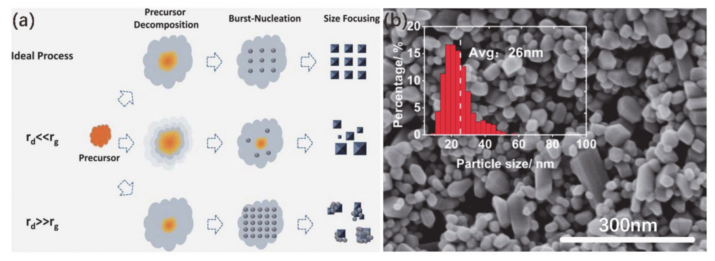
3.1.1. The Growth of VO2 Nanoparticles (NPs)

When undergoing a reversible MIT, VO2 has remarkable changes in infrared transmittance, which makes it attract much attention in the applications of the energy-saving field (e.g., smart windows) [47]. For the thermochromic smart windows based on VO2 (M), the luminous transmittance and solar energy modification ability are the two main parameters [11]. Theoretical calculation results showed that better luminous transmittance and solar energy transmittance modulation could be achieved by reducing the size of VO2 (M) NPs to smaller than the wavelength of visible light [48]. Besides, among all nanostructures, sub-100 nm 0-dimensional (0D) VO2 (M) NPs have been studied and showed excellent monodispersity and thermochromic performance.
Over the past decade, researchers have extensively studied the preparation of 0D VO2 (M) nanostructures by the hydrothermal method. However, the polymorphism of VO2 makes it hard to synthesize pure phase VO2 (M) in one step. Thus, a subsequent thermal treatment is necessary to form pure phase VO2 (M). It has been reported that VO2 (M) NPs with an average particle size less than 100 nm can be prepared by the hydrothermal method. Li et al. [49] firstly synthesized VO2 (D) NPs by using oxalic acid dehydrate as the reducing agent and polyvinylalcohol as the surfactant. Then, the VO2 (M) NPs were obtained by annealing in a vacuum environment (~20 Pa) at different temperatures for 1 h. The as-prepared VO2 (M) NPs were uniformly distributed with the average size of 70 nm.
In order to better control the size of VO2 NPs, Chen et al. [50] optimized the preparation process of VO2 NPs and synthesized high-quality VO2 NPs with smaller diameters (i.e., 25–40 nm). In this work, vanadium pentoxide and diamide hydrochloride were used as source materials. Here, the synthesis of VO2 NPs is considered to be a “heating-up” process. When the precursor was heated to the critical temperature, the precursor was instantaneously decomposed to produce excessive monomers, a highly supersaturated reaction system was formed and then a burst-nucleation process occurred. In this process, a large number of nuclei simultaneously grew and rapidly consumed monomers, which inhibited the further growth of particles.
During the process of growth, the decomposition rate of the precursor (rd) and the growth rate of the grain (rg) are two important factors that determine the particle size, as shown in Figure 3a. When rdrg, the growth of smaller grains is restricted because of the absence of monomers, which results in the polarization of grain size. If rdrg, the supersaturated monomer solution produces excessive nuclei and leads to aggregation as the concentration increases. Thus, in order to precisely control the size of NPs, it is a key point to control the rd and rg in the growth process. Finally, the hydrothermal products were annealed at a higher temperature to obtain VO2 (M). Figure 3b shows the scanning electron microscope (SEM) image of VO2 (M) NPs with good crystallinity and a relatively low average size of 23 nm. This method can provide a reference for the growth of VO2 NPs with ultra-small size.

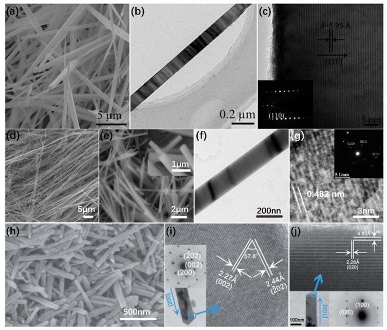
3.1.2. The Growth of VO2 Nanowires/Nanorods (NWs/NRs)

The synthesis and characterization of one-dimensional (1D) nanostructures, e.g., NWs and NRs, have attracted much attention due to their anisotropic surface properties and potential applications in integrated devices. Moreover, 1D nanostructures can offer large specific surface areas (defined as the surface area per unit volume) and efficient electron transport pathways to achieve high capacity. Thus, 1D VO2 has been extensively studied in recent years. Several studies have reported the preparation of 1D VO2, especially NWs, NRs, etc., via the hydrothermal method [33,51,52,53,54,55]. The most important feature of the hydrothermal method is that the free-standing VO2 nanostructures can be grown without substrates, which facilitates the dispersal of the NWs in further applications. It is worth noting that most of the VO2 structures synthesized by hydrothermal method are VO2 (A) or VO2 (B) [29,30,52,53,54,56]. In our previous work, single crystallized VO2 (A) NWs were synthesized by V2O5; the oxalic acid (H2C2O2·H2O) and PEG-6000 were used as the reducing agent and surfactant, respectively [29]. The morphology of VO2 (A) characterized by SEM is shown in Figure 4a. The width of NWs ranges from tens to hundreds of nanometers, and length is from a few microns to tens of microns. Figure 4b,c displays low-resolution transmission electron microscopy (LRTEM) and high-resolution (HRTEM) images of an individual VO2(A) NW. According to the figures, the spacing between the lattice fringes of 5.95 Å exactly corresponds to the distance between two (110) crystal planes of VO2 (A). With the moving of the electron beam along the NW, the selected area electron diffraction (SAED) pattern (inset of Figure 4b) remains unchanged, indicating the whole NW is single crystal. In order to form VO2 (M), the further annealing process is needed. Horrocks et al. [33] studied the synthesis of free-standing VO2 (M) via hydrothermal method in three steps. Firstly, V3O7·H2O NWs were synthesized through the hydrothermal exfoliation and reduction of bulk V2O5 by using oxalic acid dihydrate, as shown in Figure 4d. The NWs were 183 ± 34 nm in width and hundreds of micrometers in length. Then, V3O7·H2O NWs were hydrothermally reduced to form VO2 (A) and VO2 (B) NWs. Finally, the NWs mixtures of VO2 (A) and VO2 (B) were collected and then annealed at 475 °C for 1 h to crystallize into M1 phase. Figure 4e shows the SEM image of annealed monoclinic VO2 (M) NWs with the rectangular cross-section and the length of about tens of microns. The TEM image (Figure 4f) of the NWs shows the average width of 187 ± 77 nm, which is close to the width of V3O7·H2O NWs. This indicates that the morphology of VO2 (M) NWs could not be affected by the annealing process. The HRTEM image and SAED pattern of single NW confirm that the M1 monoclinic phase exists in VO2 NW, as shown in Figure 4g. Besides. Wu et al. [54] reported a controllable oxidation reaction to synthesize the highly uniform VO2 (M) NRs. Firstly, they synthesized the V(OH)2NH2 precursor by a controllable oxidation reaction of V(OH)2NH2 in formic acid (HCOOH) buffer solution [57]. Additionally, the HNO3 solution was added to the V(OH)2NH2 precursor and stirred strongly. After that, the mixture was heated at the temperature of 200 °C for 36 h. Finally, after cooling the system to room temperature, the final VO2 (M) sample was collected by centrifugation. Figure 4h shows the SEM image of as-grown VO2 (M) NRs. The diameter of NRs ranged from 30 to 120 nm, and the length was up to 400–800 nm. Figure 4i,j shows the HRTEM images of two individual VO2 (M) NRs. Insets are their corresponding SAED patterns and the morphologies of the selected NRs. The results clearly reveal the crystallographic growth model for monoclinic VO2 (M) NRs.

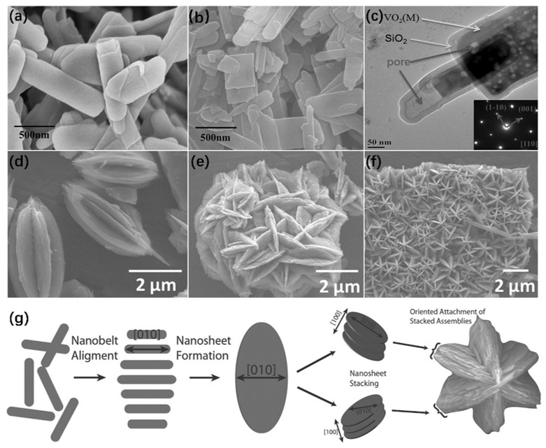
3.1.3. The Growth of VO2 Nanosheets (NSs)

The VO2 synthesized via hydrothermal method also easily forms NSs or “flower-like” structures [43,58,59]. Li et al. [58] fabricated plate-like VO2 (M)@SiO2 NSs via low-temperature hydrothermal method with post-annealing. The VO2 (B) coated with SiO2 was firstly obtained by using the modified Stober method. The length or width of VO2 (B)@SiO2 NSs was several hundreds of nanometers, and the thickness was 20–30 nm, as shown in Figure 5a. Moreover, the VO2 (M)@SiO2 NSs can be obtained from VO2 (B)@SiO2 by a heat treatment process, and the morphologies of the products are very close to the original morphology of VO2 (B)@SiO2, as illustrated in Figure 5b. The TEM image of VO2 (M)@SiO2 in Figure 5c shows that a thin layer of SiO2 was uniformly coated on VO2 (M), and numerous nanopores were formed inside. The density difference between VO2 (M) and VO2 (B) leads to the formation of nanopores. In recent years, flower-like or star-assemblies structures consisting of NSs have been investigated [60,61]. These structures have larger specific surface areas and may be used in some specific fields. Uchaker et al. used the acid reduction approach to synthesize star-assemblies of VO2 (B) mesocrystals [59], which were used as a cathodic electrode material in lithium-ion batteries. Figure 5d–f illustrates the representative individual mesocrystal assemblies and the corresponding overall SEM micrograph. The star-assemblies were evenly distributed and closely arranged. Additionally, the size of VO2 (B) NSs was about tens of nanometers. Each arm of the star assembly was separated from the other ones, indicating that it was not a single crystal structure. The VO2 (B) nanostructures reported in this work were synthesized by the following reaction: V2O5 + H2C2O4 →VO2 (B) + H2O + CO2. Oxalic acid was employed as both the reducing agent and the chelating agent. A schematic diagram of the formation mechanism of the mesocrystal is shown in Figure 5g. Firstly, VO2 (B) is treated with the solvothermal method for 4 h to form elliptical NSs. The growth direction of VO2 (B) does not change during this step. Then, several NSs are stacked together in an epitaxial manner to minimize the system’s energy. The residual chelating agent remaining on the (100) surface of each NS can effectively reduce the Debye length of the electric double layer, and the van der Waals forces between the components can be stabilized, thereby leading to the formation of the superstructure and preventing the fusion of individual NSs. After this step, several VO2 (B) NSs are stacked together to form a star-like structure.

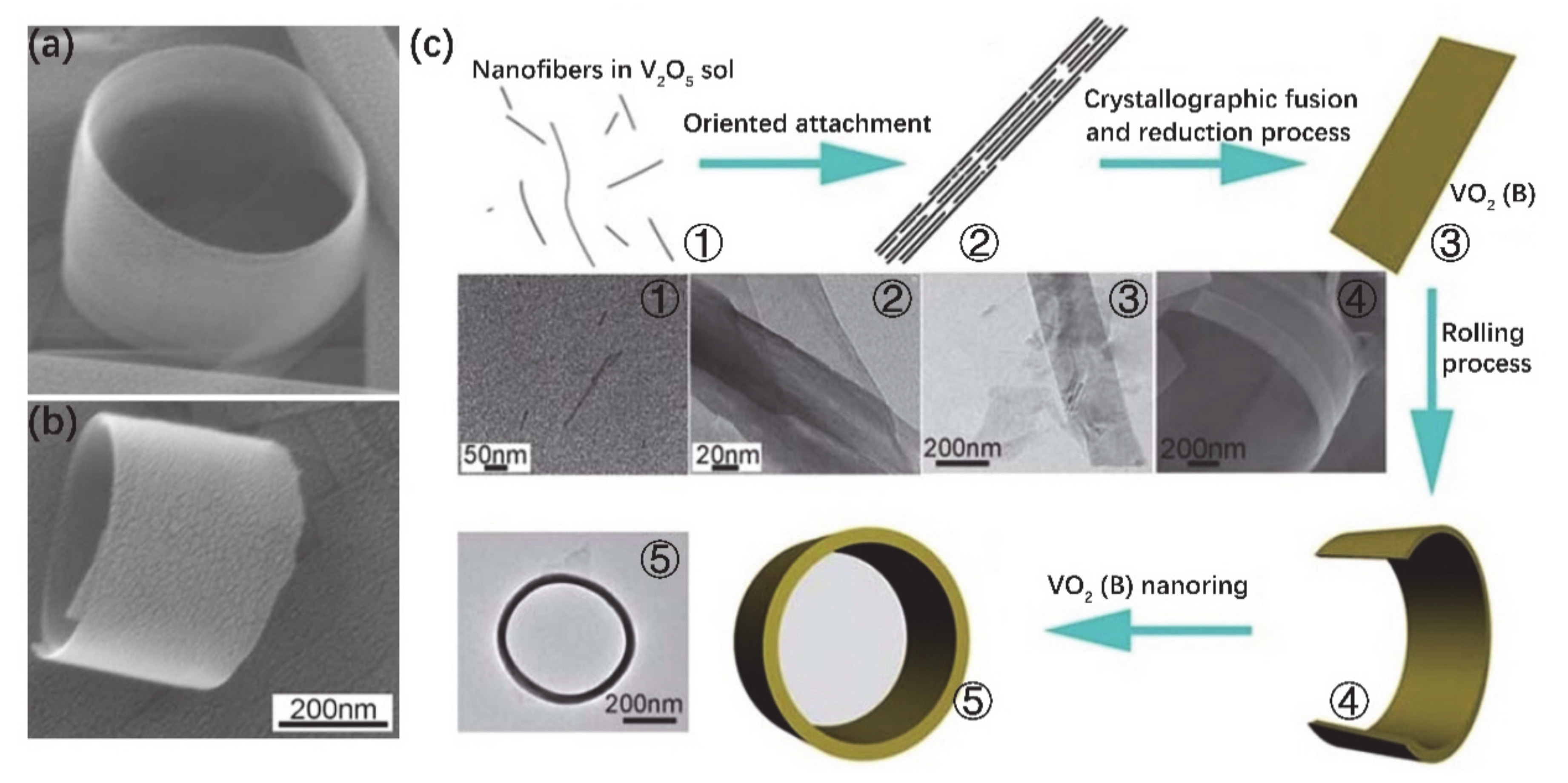
3.1.4. The Growth of VO2 Nanorings

In recent decades, it has still been a challenge to synthetize complex nanostructures, e.g., a nanoring structure. The special morphology of nanorings makes them exhibit many unusual behaviors, such as the abnormal dispersion of a magnetic field in semiconductor nanorings [62,63,64,65]. Li et al. [64] synthesized metastable phase VO2 (B) nanorings by hydrothermal treatment of V2O5 sol with PEG. PEG was employed as a surfactant and reducing agent, which is important for adjusting the length and width of VO2 NBs. It was found that proper hydrothermal conditions can accelerate the directional attachment growth of nanofibers in precursors and lead to the formation of VO2 (B) nanorings. SEM images in Figure 6a,b display different perspectives of a single VO2 (B) nanoring. The diameter and shell thickness of the as-grown VO2 (B) nanorings are 300–500 nm and 10–40 nm, respectively. The corresponding schematic diagram of formation processes is displayed in Figure 6c. VO2 (B) has a lamellar structure, and hydrothermal conditions provide a driving force for the formation of nanoring structures. In this work, PEG had a uniform and ordered chain structure (hydrophilic –O– and hydrophobic –CH2–CH2– radicals half-and-half), which is easy to adsorb on the surface of metal oxide colloids and reduces the colloid activities. With the increase of polymer absorption, the growth rate of colloids will be limited. On the other hand, the intercalation properties of V2O5 make the organic molecules easily embed in their layered structures. PEG has been employed as a surfactant and reducing agent that effectively depresses the dimension of the intermediate product. Generally, the morphology and size of as-grown vanadium oxide nanostructures depend on the growth conditions, e.g., concentration and type of template. In this work, the concentrations of V2O5 sol and PEG were modified to control the thickness and length of the VO2 (B) nanoribbons, which act as predecessors of the nanorings. Stage 1 in Figure 6c shows the fibrous structure in V2O5 sol. Under hydrothermal conditions, these tiny fibers can maintain and even enhance the spontaneous oriented growth of VO2 (B) nanoribbon. At the beginning, self-assembly of V2O5 nanofibers resulted in the formation of banded structures with limited size in the presence of excessive PEG (stage 2 in Figure 6c). With the increase of hydrothermal time, a thin single-crystal VO2 (B) nanoribbon was formed by the crystallographic melting process (stage 3 in Figure 6c). Finally, VO2 (B) nanorings were formed by the rolling mechanism of nanoribbons (stages 4 and 5 in Figure 6c).

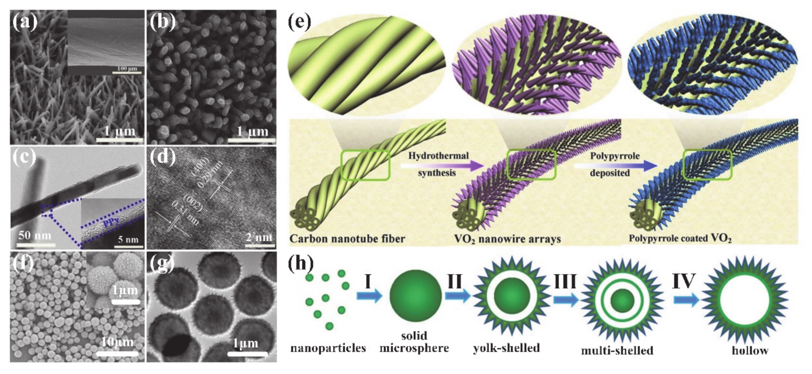
3.1.5. The Growth of Other Structures

In addition to the structures described above, some special structures, e.g., NW arrays (NWAs) and hollow microspheres, have been successfully fabricated by the hydrothermal method [66,67]. Man et al. [66] fabricated a fiber-shaped asymmetric supercapacitor (FASC) by growing aligned three-dimensional (3D) VO2@polypyrrole (VO2@PPy) core-shell NWAs on carbon nanotube fibers (CNTFs). Precursor solution and CNTF were placed together in an autoclave. The autoclave was then sealed and heated to 180 °C for 24 h. After the reaction was completed and the system was cooled to room temperature, the CNTFs covered with VO2 NWAs were removed and dried at 60 °C for 12 h. Finally, the VO2@PPy/CNTF cathode and a thin layer of nitrogen doped carbon coated vanadium nitride NWAs on CNTF anode were twisted together to form the all-solid-state FASC devices after drying. The schematic diagram of the fabrication process of the VO2@PPy/CNTF electrode is displayed in Figure 7e. Figure 7a shows that VO2 NWAs are aligned and densely distributed on the whole surface of the CNTF (inset of Figure 7a). Additionally, Figure 7b shows a SEM image of VO2@PPy NWAs. The TEM image in Figure 7c indicates that the VO2@PPy is a core-shell structure. VO2 NWA is continuously coated by a PPy thin shell with a thickness of 2–3 nm. In addition, HRTEM image in Figure 7d shows that the fringe spacings are about 0.29 and 0.31 nm, which correspond to the (400) and (002) planes of monoclinic VO2, respectively.
In recent years, hollow micro-nanostructures have attracted great interest due to their wide applications in many fields [68,69,70]. A great deal of work has reported the synthesis of hollow structures with different internal structures, which are attractive for many applications, e.g., drug delivery [71], photocatalysis [72], dye-sensitized solar cells [73], gas sensors [74] and lithium-ion batteries [67]. Pan et al. [67] synthesized various uniform VO2 microspheres with different hollow structures, e.g., yolk-shell, multi-shell and single-shell structures, via hydrothermal method. Figure 7f,g shows the SEM and TEM images of as-grown VO2 microspheres. The surface of a microsphere consists of small nanoplates with a thickness of about 20 nm. VO2 microspheres have a yolk-shell structure, and the shell thickness and spherical core diameter are 100 and 400 nm, respectively. Figure 7h shows the growth route of the VO2 microspheres and the corresponding structural evolution. Firstly, VOC2O4 was hydrolyzed as vanadium oxide NPs, and then they were fused to form solid microspheres in stage I. After that, the solid spheres underwent the inside-out Ostwald-ripening process for the first time and transformed into yolk-shells in stage II. With increase the solvothermal reaction time, the pre-formed solid cores underwent the secondary Ostwald-ripening process and transformed into a multi-shelled structure (stage III). Finally, the unstable internal structure was completely dissolved and recrystallized to form the hollow microspheres.

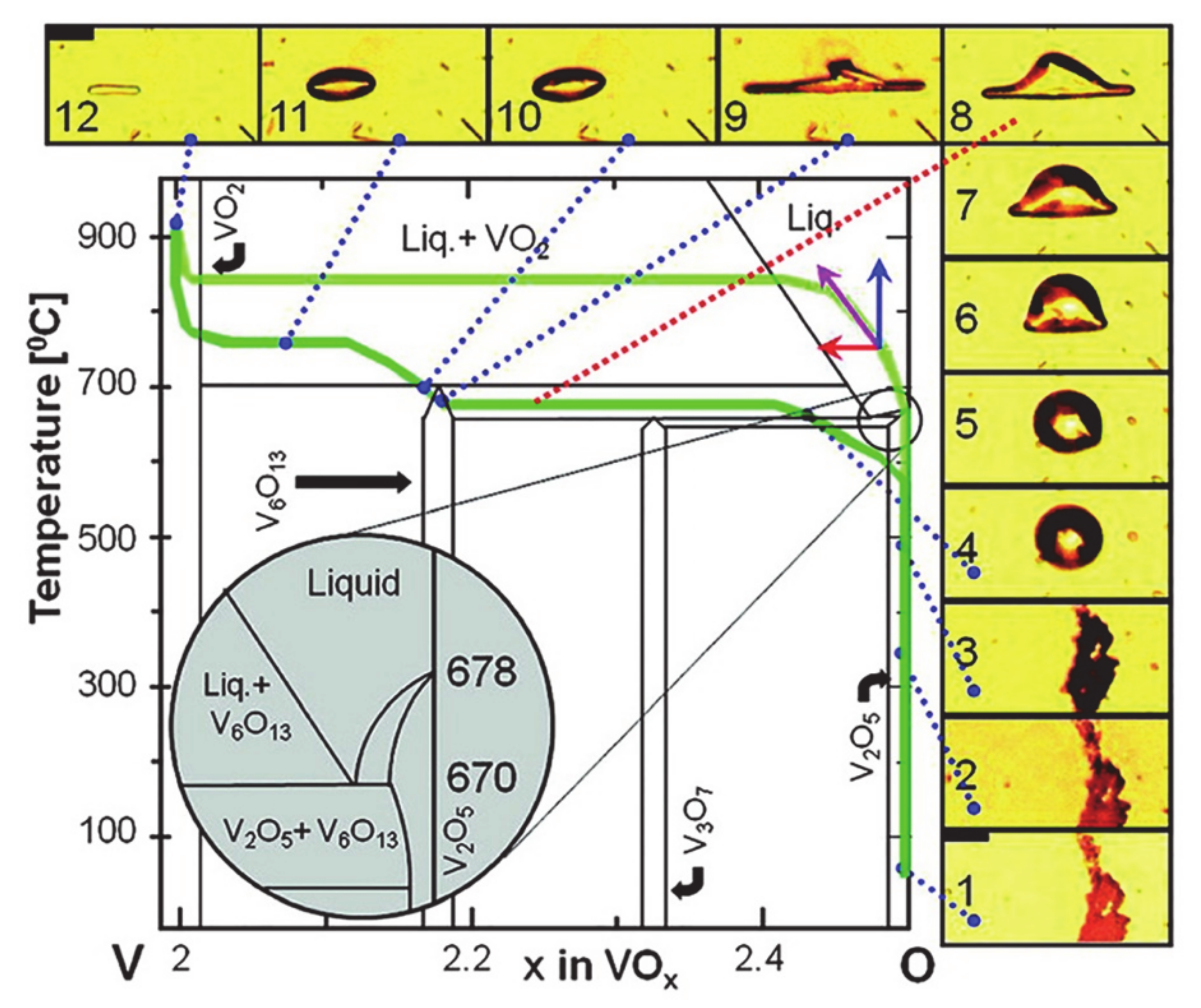
3.2. Chemical Vapor Deposition (CVD)

CVD is a chemical vapor reaction growth method that is one of the most commonly used deposition technologies. The CVD method can be traced back to 1945 when it was used to deposit TiC hard coatings. Generally, during the process of the chemical vapor reaction, a variety of reactants are gasified at high temperatures and then are carried by carrier gases to the surface of the substrate in the reaction chamber. Finally, the products are deposited on the surface of the substrate and grow into a thin film or other nanostructures. The deposition parameters of CVD, i.e., the types of gases, gas flow, reaction time, temperature and heating–cooling curve, have significant effects on the morphology and quality of the products. Among them, temperature is the most important factor. Too high a deposition temperature would cause the phenomenon of coarse grains. On the contrary, too low a temperature would cause an incomplete reaction, resulting in unstable structures and intermediate products, and a decrease of the bonding strength between products and substrates. Therefore, it is very important to set reasonable parameters during the growth process of materials. Various materials, including oxides, nitrides, carbides and elemental substances, can be deposited by CVD. In recent years, the growth of VO2 films and NWs by CVD method has been established.

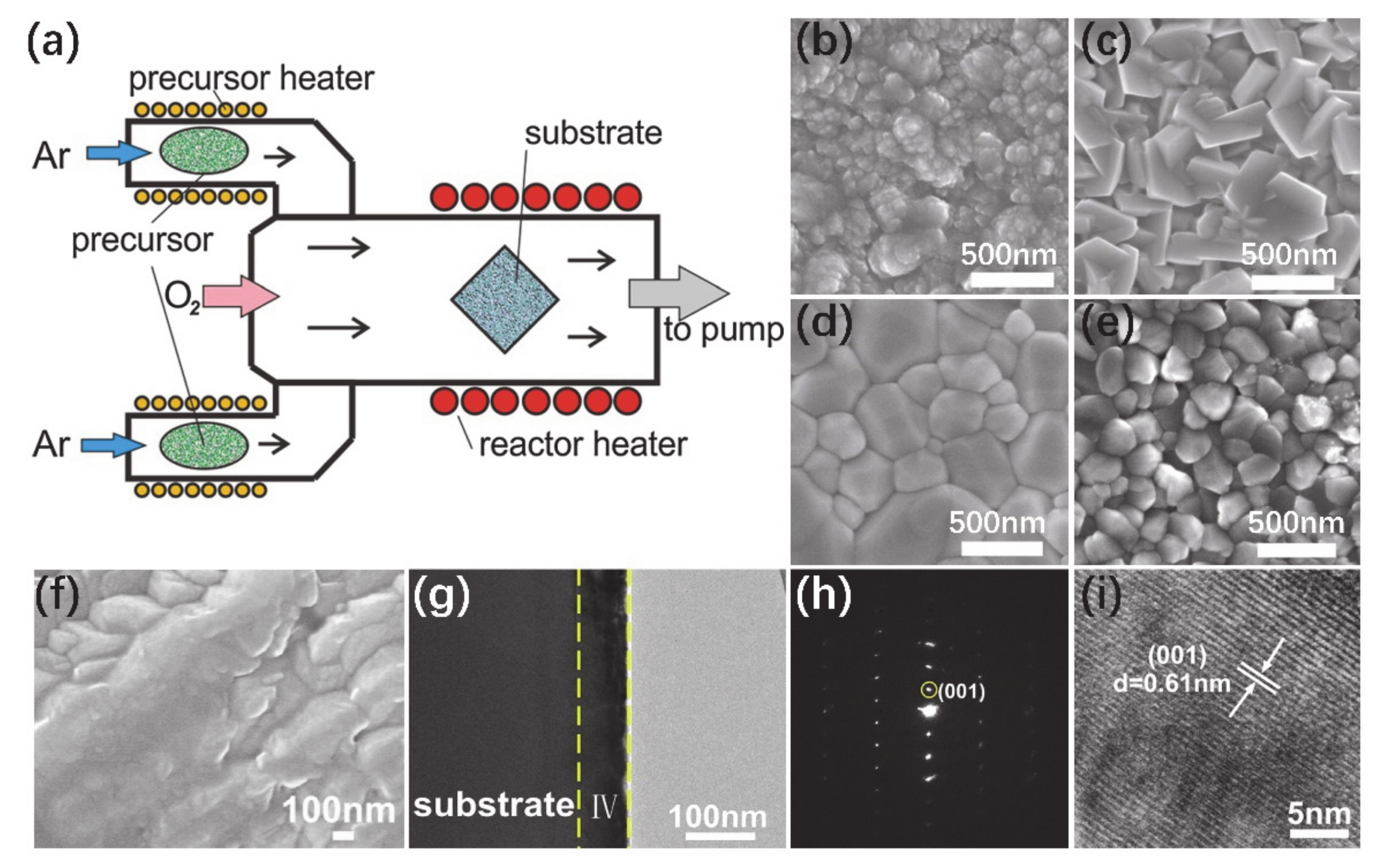
3.2.1. The Growth of VO2 Thin Films

V(C2H7O)4, VOCl3, VCl4, VO(OC3H7)7 and V(C5H7O2)3 are usually used as source materials to synthesize VO2 by CVD method. Yakovkina et al. [75] prepared VO2 (M) thin film by metal–organic CVD (MOCVD). They used VO(acac)2-VO(C5H8O2)2 as the precursor and SiO2/Si(111) as the substrate. The flow rate ratio of argon/oxygen was controlled at 3–10 standard cubic centimeters per minute (sccm). The precursor source temperature was controlled in the range of 120–150 °C, and substrates were maintained at 390–490 °C, respectively. The whole growth process lasted for 30–120 min. The scheme of the CVD reactor for the growth of VO2 film is shown in Figure 8a. Compared with traditional CVD, MOCVD provides low temperature and low-pressure growth without post-growth annealing, and a shorter growth process. Sectional heating effectively avoided incomplete reactions of source materials. The morphologies of films with different grain sizes were obtained by adjusting the temperatures of the substrates, as shown in Figure 8b–e. The VO2 (B) phase mixed with the VO13 mesophase was obtained at low temperature (Figure 8b), and VO2 (M) monoclinic phase was obtained at a high temperature. CVD is a good way to synthesize not only pure phase VO2 (M) but also co-doped thin films. Guo et al. [76] reported Mo-Al-doped VO2 (B) thin films by CVD. V(C5H7O2)3 was employed as a V source mixed with Mo acetylacetonate ([CH3COCH=C(O)CH3]2MnO2) and Al acetylacetonate (Al(C5H7O2)3). The deposition processes were carried out in a three-zone furnace. The temperatures of precursor and substrate were 170 and 400 °C, respectively. The SEM image of Figure 8f shows large particles of Mo-Al-doped VO2 (B) thin films. The corresponding cross-sectional TEM images, SAED patterns and HRTEM images in Figure 8g–i indicate that the film is well crystallized along (001) direction.

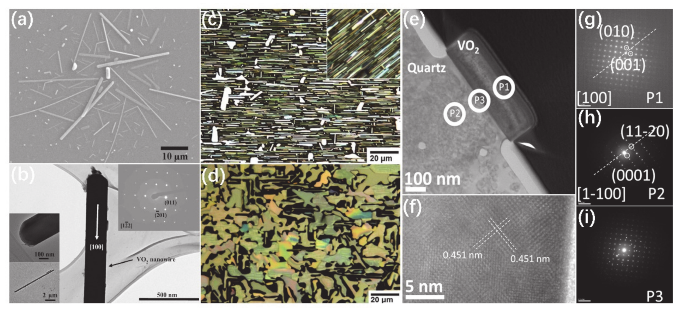
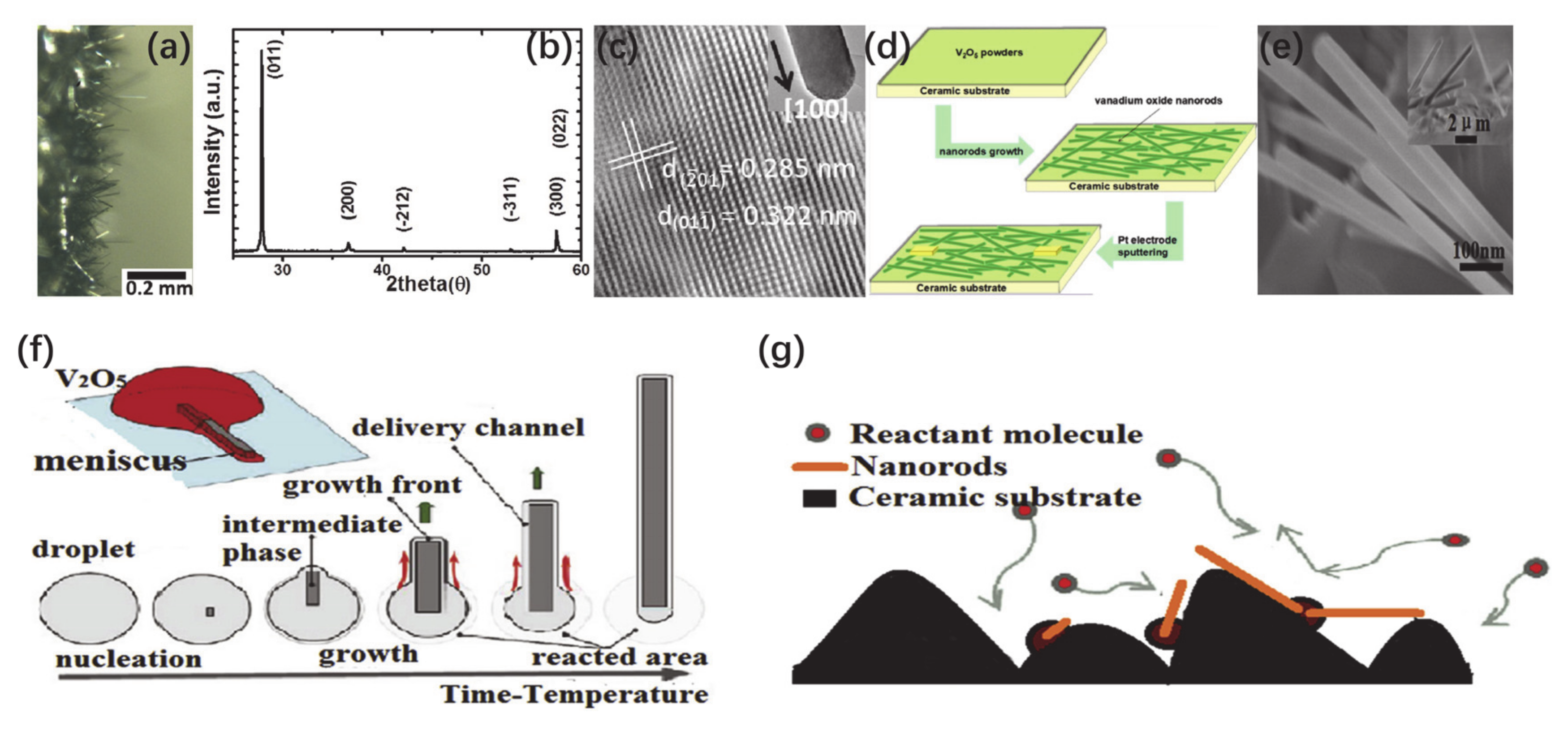
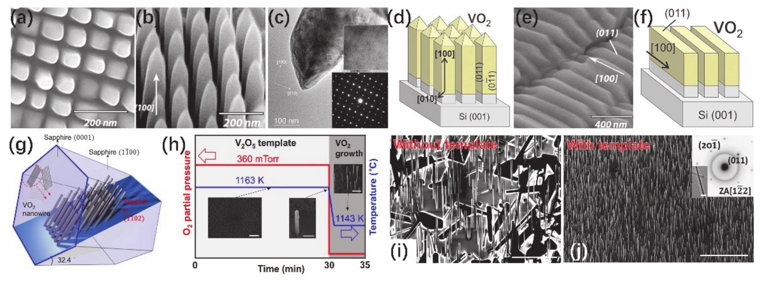
3.2.2. The Growth of VO2 Nanowires (NWs)

In 2004, Guiton et al. firstly synthesized VO2 (M) NWs via CVD method by employing VO2 powders as the evaporation source [77]. The evaporation of VO2 usually requires a high temperature of more than 1000 °C. Therefore, the low melting point of V2O5 (690 °C) is commonly chosen as the reaction source to effectively decrease the deposition temperature. The phase diagram in Figure 9 summarizes the growth trajectories of VO2 (M) NWs prepared under different conditions [78]. During the CVD synthesis process, heating rate and oxygen loss rate are important factors that can determine the growth paths of VO2 NWs (green and light green paths in phase diagram). When the reaction source V2O5 powers are in a very low oxygen pressure environment and the heating rate reaches ~500 °C/min, VO2 NWs crystallize directly from the molten V2O5 precursor; see the light green path in Figure 9. On the contrary, under a lower heating rate, the precursor of V2O5 would first form V6O13 crystals at an insufficient temperature because of the lack of power to form VO2 nuclei and the slow loss of O. With the increase of temperature, V6O13 melts into droplets and becomes saturated. Finally, VO2 NWs are crystallized out.
In recent years, the synthesis of VO2 NWs via CVD has been extensively studied [12,19,77,79,80]. Maeng et al. [81] reported a deposition process of VO2 NWs by using Si3N4/Si or molybdenum grid as the substrates. Figure 10a shows the SEM image of VO2 NWs. One can see that NWs are randomly distributed on the substrate and have different lengths. The SAED image in Figure 10b indicates that VO2 NWs were grown with different orientations. The random growth of NWs is directly related to the choice of substrates. Chen et al. [82] synthesized the horizontally aligned VO2 NWs on polished quartz with x-cut (1–100) direction, which can provide a dense growth mode of VO2 NWs. The deposition temperature has been controlled for growth of horizontally aligned NWs and microplates, as shown in Figure 10c,d. The HRTEM and SAED images indicated that the growth of NWs is along the (1–100)quartz direction, as illustrated in Figure 10e–i. The temperature plays an important role in the control of the diameters and densities of VO2 NWs. VO2 NWs grown at low temperatures have small diameters and low density. On the other hand, high temperatures lead to the fusion of NWs and promote their lateral growth, resulting in the formation of a microplate nanostructure. The embedded VO2 microplates grown in the substrate have irregular shapes of sub-micron thickness and tens of a micron in size. Due to the elastic strain from the substrate, rich domain patterns are exhibited in the VO2 microplates, as shown in Figure 10d. One can see that substrate and temperature can directly affect the morphology of VO2.
In addition, Chen et al. [83] synthesized ultra-long, ultra-dense and free-standing VO2 micro/nanowires by using the unpolished rough surfaces of quartz substrates. Figure 11a shows the optical image taken from the side view, which indicates the VO2 NWs are free-standing and randomly dispersed on the substrate. The corresponding X-ray diffraction (XRD) pattern in Figure 11b shows that except the {0kl} peak of VO2 in-plane growth, there are abundant peaks of (200), (212), (311), (300), etc., which indicate the independent random orientation and non-epitaxial growth of VO2 NWs. The TEM image in Figure 11c demonstrates a smooth surface and a monoclinic structure of VO2 NWs. Similarly, Liang et al. [84] synthesized free-standing VO2 NWs by using rough surfaces of a ceramic substrate, as shown in Figure 11e. The preparation schematic diagram of VO2 NWs is shown in Figure 11d. V2O5 powder was employed as the evaporation source and was uniformly placed on a rough-surface substrate. The substrate for depositing products was placed in the range of 0.5 cm from the evaporation source. Besides, the growth mechanism of free-standing VO2 NWs was investigated, as described in Figure 11f,g. Under a high temperature, the V2O5 reaction source firstly melts into droplets. Such a liquid phase promotes the growth of nanostructure and then transports materials to the growth front. During the process of nanostructure growth from host droplets, a thin liquid film wets the nanostructure along the length direction to create a material transport channel for the growth of the NWs. Finally, the droplets are completely depleted and VO2 NWs are formed, as shown in Figure 11f. The rough surfaces of substrates (quartz, ceramic) provide favorable nucleation sites for NWs (as shown in Figure 11g). The dense nucleation sites lead to the formation of dense NWs. After the nucleation of NWs, the capillary force begins to appear at one end. The exposure of NWs to the reactive molecular atmosphere makes it easy to obtain the molecules needed for growth, so NWs can grow up to hundreds of microns in length.
Up to now, most VO2 NWs have been randomly distributed on the substrates and show random sizes and varied directions during the synthesis process. Mutilin et al. [85] reported the growth of single crystal VO2 NW arrays on Si (001) substrates with controllable size, spacing and orientation. A large-area double nanoimprint lithography (NIL) technique was employed to obtain periodic gratings printed on a Si surface. Figure 12a,b shows the top- and side-view morphologies of the synthesized VO2-on-Si nanostructures. The TEM image and SAED pattern from Figure 12c demonstrate the smooth surface and monoclinic structure of VO2 NWs. Moreover, horizontal VO2 NWs or nanowalls were also observed in some regions, as illustrated in Figure 12e. The insufficiency of the presswork at the second NIL stage resulted in the strips on Si, and then those VO2 NWs or nanowalls were grown on Si strips. Figure 12d,f shows the schematic diagrams of arrays of VO2 NWs and nanowalls, respectively. In addition, Wang et al. [86] proposed a novel approach for growing vertical-arranged VO2 NW forests via defect engineering. The design schematics of the VO2 NWs hybrid material system are depicted in Figure 12g. Sapphire (Al2O3) has been chosen as the appropriate substrate for the growth of aligned VO2 arrays. The freestanding strain-free VOx compound can be obtained by using the r-plane sapphire substrate. Choosing r-sapphire can also ensure a high nucleation rate and denser VO2 NW arrays. In this work, they designed a two-step, self-templated growth of VO2 NWs using V2O5 as the precursor, as shown in Figure 12h. The two steps of growth were as follows: (i) V2O5 droplets were grown as a template on r-plane sapphire; (ii) VO2 NWs were separated out from droplets to form neatly arranged NWAs. In the first stage, the carrier gas with a certain oxygen/argon volume ratio was used to create an oxygen-enriched environment to prevent the formation of vanadium with reducing (+3 and +4) valences. Regarding the other aspect, a much higher temperature (1163 K) than the melting point of V2O5 was employed to prevent its large-scale growth without leaving a molten droplet of V2O5 on the substrate. At the second stage of the growth, oxygen supply was suddenly interrupted and growth temperature was slightly reduced, which provided a greater supersaturation for VO2 growth. During this stage, the V2O5 droplet was a natural template for VO2 growth, so that more atoms could be adsorbed and vertically-arranged VO2 NW forests could be fabricated. As a contrast, the pure argon was used as the carrier gas, a continuous deoxidation process occurred at high temperatures and the growth was carried out without template. Top views of grown VO2 NW arrays without and with V2O5 template and two-stage process are compared in Figure 12i,j. The density of NWs varies greatly, and the reduction of redundant growth in the plane can be easily identified. Additionally, the inset of Figure 12j shows a TEM image and the SAED pattern of a single VO2 NW.

3.3. PLD

PLD can be dated back to the 1960s and was developed with the invention of a pulsed laser source and the discovery of high-temperature superconductivity. After decades of development, the range of materials that can be prepared by PLD is expanding greatly. PLD can be used to fabricate thin films ranging from monoatomic layers to quasi-bulk material. It occupies an irreplaceable position in fabrication of thin film [87]. In the PLD process, a high-power pulsed laser is focused on the surface of a target in a high vacuum chamber and the surface of the target is ablated to form plasma plume, which consists of target molecules and is deposited on the substrate to form thin film or other nanostructures. The rapid melting and evaporation of target under high-energy laser in a small area lead to all elements in the target evaporate at the same time. Therefore, it is easy to obtain multicomponent thin films with a stoichiometric ratio of target materials by the PLD method. In addition, PLD has the advantages of low temperature, high growth rate, in situ growth, etc. Moreover, the preparation parameters are easy to be adjusted, and there is no restriction on the types of target materials. Besides, it is convenient to prepare multilayers and superlattices by PLD.

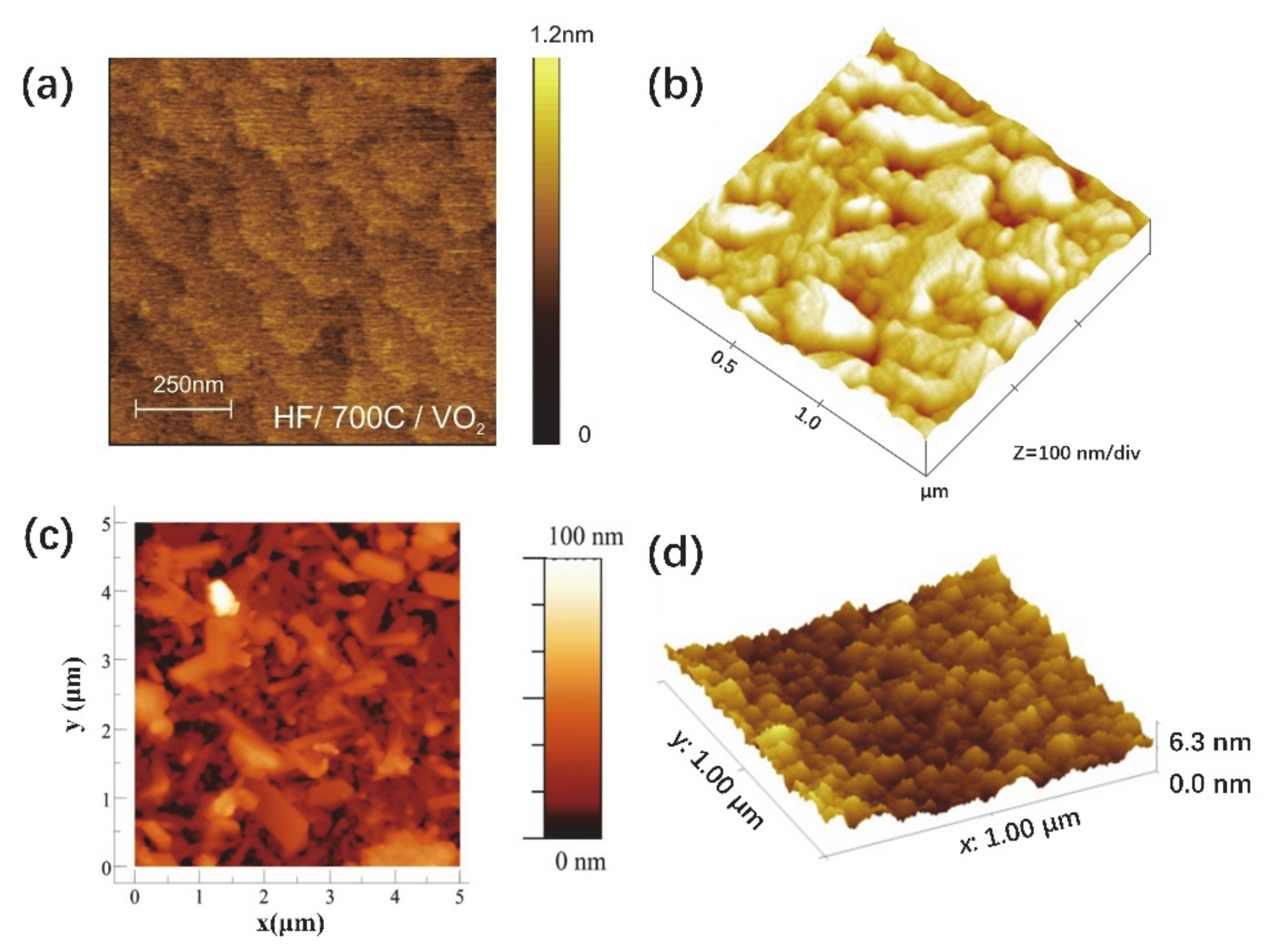
3.3.1. The Growth of VO2 Thin Films

Nowadays, a lot of studies have attempted to fabricate the VO2 thin film by PLD. TiO2 [88], Al2O3 [89,90], glass [91,92], Si/SiO2 [93], etc., are usually used as substrates in the PLD fabrication of a VO2 thin film. V2O5 [94], V2O3 [95] and VO2 [96] are usually used as the target materials. High-quality thin films can be obtained by adjusting the parameters of gas pressure, target-substrate distance, laser energy, deposition and annealing temperature. Figure 13 shows AFM images of VO2 thin films deposited on TiO2, Al2O3, Si/SiO2 and glass substrates. As is well known, the high-temperature metal phase of VO2 (R) has the same crystal structure and space group as rutile TiO2; thus, TiO2 is usually used as a substrate in the deposition of VO2. Figure 13a shows the AFM image of a VO2 thin film deposited on TiO2 (001) [88]. Here the TiO2 substrate was etched by HF and annealed at 750 °C in an oxygen environment to form terraces. Terraced VO2 thin film with atomic-level smoothness was epitaxially grown on the TiO2 substrate. On the other hand, VO2 is monoclinic and pseudo-hexagonal at room temperature. Therefore, hexagonal Al2O3 is also an ideal substrate for the growth of an epitaxial VO2 thin film, and the lattice mismatch is within a few percentage points [97]. As a contrast to traditional deposition techniques with high-temperature deposition, a VO2 thin film can be fabricated on c-cut (0001) Al2O3 substrate at room temperature by using PLD [90]. The surface of a VO2 thin film is shown in Figure 13b, and it indicates that the RMS roughness of VO2 thin films is about 4.5 nm [90]. Glass substrates have advantages in cost and industrial applications, especially in smart windows. Previous work also has attempted to fabricate the VO2 thin film on a glass substrate [92], as shown in Figure 13c. For the deposition of VO2 on a glass substrate, different VO2 phases (e.g., M1 phase and B phase) can be obtained by adjusting the deposition temperature [92]. From the AFM image of VO2 thin film in Figure 13c, the roughness is about 10 nm. As the most commonly used substrate, Si/SiO2 substrate is usually used for depositing the VO2 thin film [93]. The VO2 thin film deposited on Si/SiO2 substrate exhibits dense and continuous crystalline nanostructures, as shown in Figure 13d. The roughness of as-grown VO2 thin films is about 0.671 nm. This demonstrated that the VO2 thin film deposited on Si/SiO2 substrate has a good surface morphology. Importantly, in this work, the results have demonstrated that the oxygen partial pressure has significant effects on the microstructures of the films [93].

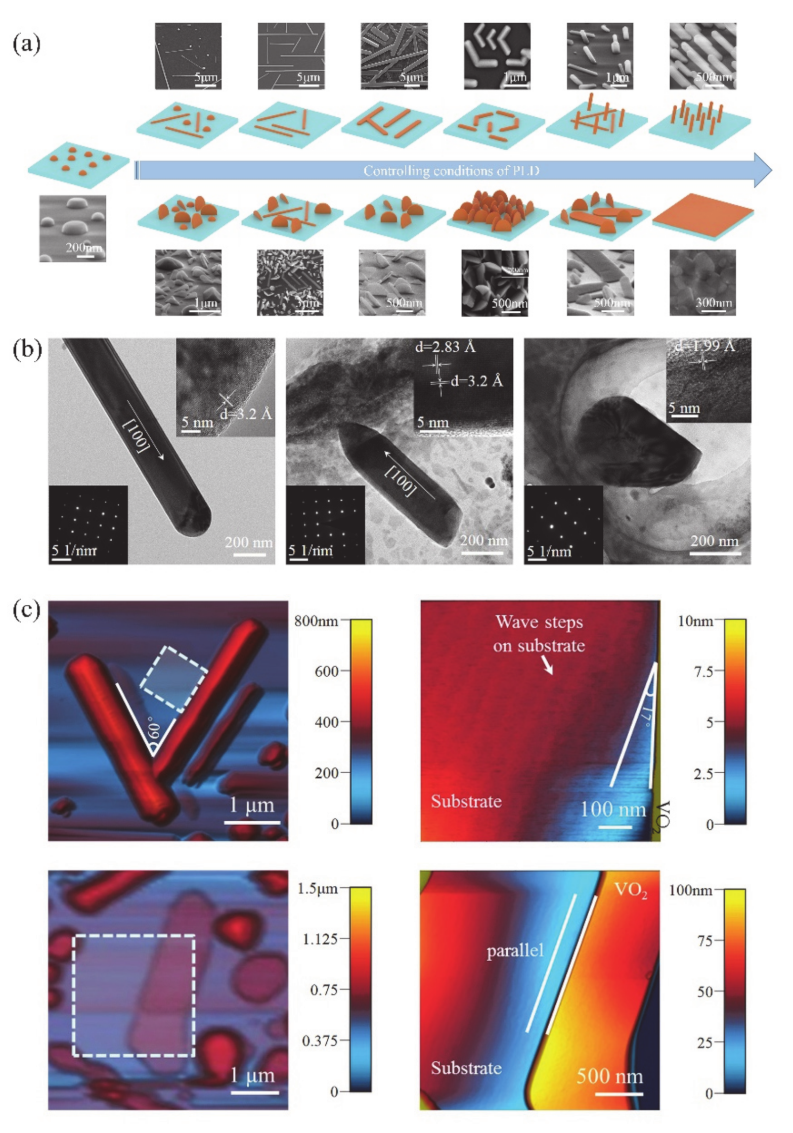
3.3.2. The Growth of VO2 Low-Dimensional Structures (LDSs)
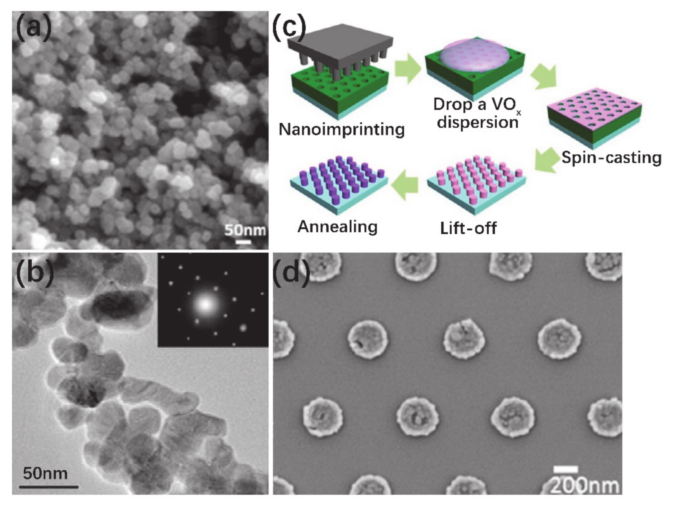
As is known to all, PLD is an excellent method for depositing thin film structures. Interestingly, under certain deposition conditions, it is also an effective approach to fabricate LDSs. In our previous work, by controlling the deposition conditions (e.g., substrate, oxygen pressure, deposition and annealing temperatures, pulse count and energy of laser, the distance between the target and substrate, etc.), numerous LDSs of 0D NDs, 1D NWs, NBs and NRs; two-dimensional (2D) nanoplatelets; ultra-thin films; and also various mixed structures were fabricated [16]. Figure 14a shows the schematic diagrams and corresponding SEM images of as-deposited LDSs. In this work, the substrates of (0001) Al2O3, (10–10) Al2O3, (0001) SiO2 and Si/SiO2/Pt were employed to deposit the VO2 structures. The results demonstrate that the NWs and NBs are favored to grow on (0001) Al2O3 and (001) SiO2 substrates, respectively. The angle between the two NWs grown on (0001) Al2O3 substrate is 60° (or 120°). On the other hand, the nanoplatelets tended to grow along the step-terraces of the substrate (Figure 14c). Besides, the length/diameter ratio of NW can be conveniently controlled by adjusting the oxygen pressure. Interestingly, vertically-grown NWs and nanoplatelets were also obtained by controlling the pulse number of the laser and annealing treatment process. HRTEM images and SAED patterns indicate that the NW, vertically-grown NW and nanoplatelets have high crystallinity, as shown in Figure 14b. Moreover, the temperature-dependent Raman spectra and XRD patterns reveal that the MIT properties of VO2 LDSs and the mismatch strain between LDSs and substrate lattice are closely related. Therefore, PLD can be employed as a simple and controllable technique to fabricate VO2 LDSs.

3.4. Sol–Gel Method

The sol–gel method can be traced back to the middle of the nineteenth century [98], also known as the chemical solution deposition (CSD) or liquid-phase sol–gel (solution-sol–gel, SSG) method. The inorganic polymer sol–gel method is one of the most commonly used material synthesis technologies. In general, metal alkoxides are dissolved in appropriate organic solvents, and then undergo hydrolysis and polymerization to form sol. Sol further loses most of the solvent to form a gel with a continuous three-dimensional network structure. Finally, ultrafine powders, fibers and films can be prepared after heat treatment. Since the invention of sol–gel method, it has developed rapidly and has been widely employed for preparing various structures of material, e.g., bulk, powder, porous material, fibers and films. The sol–gel method has the merits of low cost and large area deposition. Most importantly, the sol–gel method is a chemical synthesis approach, so it can easily control the stoichiometry and the element doping.
It was reported decades ago that VO2 thin films can be synthesized via sol–gel method [99,100,101,102]. The synthesis of VO2 by the sol–gel method usually consists of spin-coating or dip-coating and an appropriate annealing process [102,103]. In recent years, VO2 thin films [99,104,105], nanopowders [106] and nanopillars [107] have been successfully synthesized. Importantly, sol–gel can be conveniently used for synthesizing doping VO2 structures, e.g., W-doped [103,108], Au-doped [109] and Mo-doped [110] thin films. Wu et al. [104] coated the sol solution on an Al2O3 (0001) substrate and obtained high-quality VO2 thin film after an appropriate annealing process with a uniform grains size about 100 nm. As mentioned above, VO2 NPs of small size have great advantages in the application of smart windows, and VO2 NPs with an average size of 26 nm have been prepared by hydrothermal method (Figure 3b) [50]. By combining the sol–gel and hydrothermal methods, the size of VO2 NPs is expected to be further reduced. Ji et al. [106] synthesized high-quality single crystal VO2 nanopowders by using V2O5·nH2O sol as a vanadium precursor, which was prepared by the dissolution reaction of V2O5 in H2O2. By pre-reduction and hydrothermal treatment, the VO2 nanopowders with an average size of less than 20 nm were obtained. Figure 15a,b shows the SEM and TEM images of VO2 nanopowders, respectively. The inset of Figure 15d illustrates the SAED pattern for one nanoparticle, which indicates that the monocrystalline VO2 nanopowders were obtained. Besides, VO2 nanostructure arrays also can be fabricated by using the sol–gel method assisted by templates (polystyrene spheres or nanoimprint lithography) [107,111]. VO2 nanoparticle, nanodot and nanonet arrays have been fabricated by the nanosphere lithography technique in different growth conditions [111]. Similarly, Paik et al. [107] used nanoimprint lithography to fabricate a VO2 nanostructure; the schematic diagram is illustrated in Figure 15c. Firstly, the size and the shape of nanoimprint patter were designed, and the nanoimprint lithography was employed to realize the corresponding polymer resist template. Then, the colloidal nanocrystals were spin-coated on top of the patterned template. After that, the polymer resist was lifted off and the nanopillars were successfully prepared after annealing process, as shown in Figure 15d.
On the other hand, as we mentioned before, it is a challenge to synthesize high quality epitaxial VO2 films due to the multivalence states of V element (V2+, V3+, V4+, or V5+). However, the sol–gel method (or chemical solution) can conveniently modulate the oxygen stoichiometry in vanadium oxide. In previous work, a VO2 thin film with enhanced MIT properties was synthesized by using a moisture-assisted chemical solution method [112]. In order to obtain high performance VO2 films, it is very important to prevent the formation of V5+ or V3+ during the growth process. Liang et al. [112] introduced the moisture in synthesis process and found that the moisture can significantly inhibit the formation of V5+ or V3+. Intrinsically, moisture is employed to provide oxygen vacancy in the preparation of oxides [113], which is expected to inhibit the formation of V3+ ions. Meanwhile, moisture is not active enough to oxidize V4+ ions to V5+ ions. Therefore, the oxygen stoichiometry of VO2 can be precisely control and then the enhanced MIT performance of a VO2 thin film can be obtained.

3.5. Other Methods

In addition to the methods described above, there are several other methods also can be used for fabricating VO2 nanostructures, such as magnetron sputtering [8,114,115], electrospinning [42] and MBE [116,117,118].

3.5.1. Magnetron Sputtering

Magnetron sputtering began in the 1970s and developed rapidly because of its compatibility with microelectronic manufacturing technology [119,120]. In magnetron sputtering technology, incident ions (charged particles) obtain high energy under high-voltage electric fields in a vacuum and bombard the target surface. Target atoms get enough energy from the high-energy incident ions and escape from the target surface, and then deposit on the substrate to form a thin film. Differently from ordinary ion sputtering, the movement tracks of high-energy ions are controlled by a magnetic field, which can significantly promote the lifetime of incident ions and sputtering rate. Magnetron sputtering is a common technology for the preparation of thin films. Yu et al. [121] reported the fabrication of VO2 thin films with two steps. In the first step, pure vanadium thin films were deposited on a sapphire substrate by DC magnetron sputtering and then oxidized in a pure oxygen environment. Figure 16a–f displays the SEM images of the VO2 thin films with several oxidation conditions; the insets show the grain size distribution. Obviously, the oxidation conditions, e.g., temperature and oxygen flow rate, play important roles in the grain size, shape and arrangement [122].

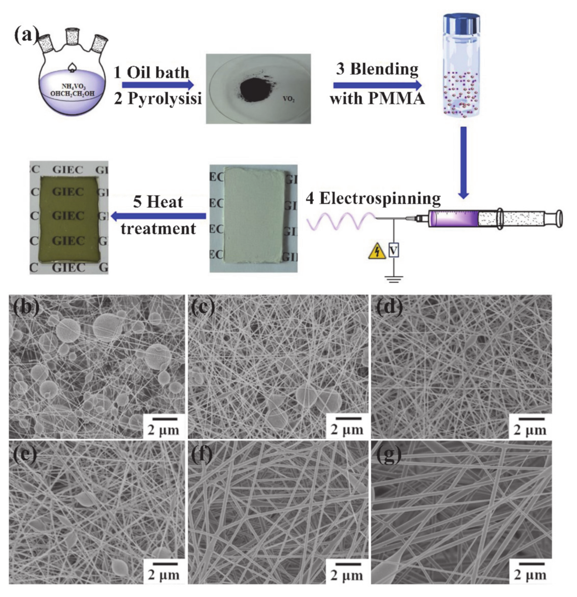
3.5.2. Electrospinning

Electrospinning is a method to form fibers from a molten polymer or polymer solution under the application of a high voltage electrostatic field. In a high voltage electrostatic field, the charged molten polymer or polymer solution undergoes a series of static spinning processes, such as spraying, stretching, splitting, solvent evaporation or solidification, and finally forms precursor nanofibers. Electrospinning is one of the most important methods for preparing nanofibers. Synthesis of V2O5/poly (vinyl acetate) by electrospinning followed by thermal treatment was reported dozen years ago [123]. Recently, Lu et al. [42] successfully prepared opaque VO2-based composite nanofibers on glass substrates by electrospinning technique. Then, a VO2 (M) thin film was obtained after heat treatment. Such a thin film of woven fibers could be used in the application of transparent thermochromic smart windows. Figure 17a describes the detailed procedures of transparent VO2 thin films via the electrospinning technique. The procedures include synthesis of VO2 NPs (stages 1 and 2), preparation of PMMA-VO2 electrospun composite nanofiber (stages 3 and 4) and heat treatment (stage 5). From Figure 17b–g, the morphologies of PMMA nanofibers vary with the concentration of polymer, which is due to the different viscosities and conductivities of the solutions [124].

3.5.3. Molecular Beam Epitaxy (MBE)

MBE is a technique for epitaxial growth of single crystal thin films with several atomic layers. The emergence of the MBE technique has had a tremendous impact on materials science. MBE equipment works in an ultra-high vacuum environment to prevent the effects of impurities. There are various elemental source furnaces and substrate heaters in the chamber with an ultra-high vacuum. Atoms or molecules in the heated source furnace will be ejected from the source furnace when opening the source furnace switch valve. Due to the van der Waals forces, the ejected atoms or molecules will combine with each other on the surface of the substrate to form a stable ultrathin film. For the fabrication of the VO2 films by using MBE, the challenge comes from the control of V and O beam flux in stoichiometric. It is difficult to control the evaporation of V source due to its high melting point and low saturated vapor pressure. In addition, V has numerous chemical valence states and its chemical valence is sensitive to the oxygen pressure. Fu et al. [116] fabricated a high-quality, pure M phase VO2 thin film by precisely controlling the V and O stoichiometric ratio in MBE deposition. The obtained VO2 (M) epitaxial film on Al2O3 (0001) substrate had a smooth surface, uniform thickness and uniform phase transformation performance [116]. Besides, Paik et al. [117] prepared ultrathin VO2 thin films by the MBE method on TiO2 (001) substrate. The thickness of VO2 thin film can be decreased to 1.5 nm. MBE is an excellent way to grow an ultra-thin VO2 thin film compared with other techniques.

3.6. Summary

The strategies for the growth of VO2, containing the hydrothermal method, CVD, PLD, sol–gel, magnetron sputtering, electrospinning, MBE, etc., are introduced in this section. The hydrothermal method is a useful method for fabricating the polymorphs of VO2 (e.g., VO2 (A), VO2 (B), VO2 (C), VO2 (D), VO2 (P) and VO2 (M)) and various LDSs of VO2 (e.g., NPs, NWs, NRs, nanorings and microsheres). The advantage of a simple process and high yield made hydrothermal method become a popular approach for the growth of VO2. CVD is mainly used for the growth of VO2 NWs. Compared with the hydrothermal method, the VO2 NWs synthesized by CVD usually have a larger length-to-diameter ratio. Besides, CVD can be also used for depositing VO2 thin films by controlling the deposition conditions. For the growth of VO2 thin films, PLD, magnetron sputtering and MBE are popular methods to realize the high-quality film. MBE is a technique for the epitaxial growth of ultrathin VO2 films. PLD is not only a simple way to deposit a VO2 thin film, but also an effective method to fabricate various LDSs, e.g., NDs, NWs, NBs, NRs and nanoplatelets. Sol–gel and electrospinning technologies can be used to synthesize VO2 thin films and nanofibers, respectively. To be clearer, the advantages and weaknesses of the mentioned preparation methods of VO2 have been listed and compared in Table 2.

4. Properties and Related Applications of VO2

Due to the excellent MIT behaviors and near-room-temperature Tc, VO2 has great potential applications in electronics (e.g., electronic switches, field-effect transistors and memories), optical devices and various sensors. In recent years, researchers have explored the applications of VO2 by utilizing the unique response characteristics of VO2 to external stimuli. Here, we briefly summarize the latest application progress of VO2.

4.1. Electrical Devices

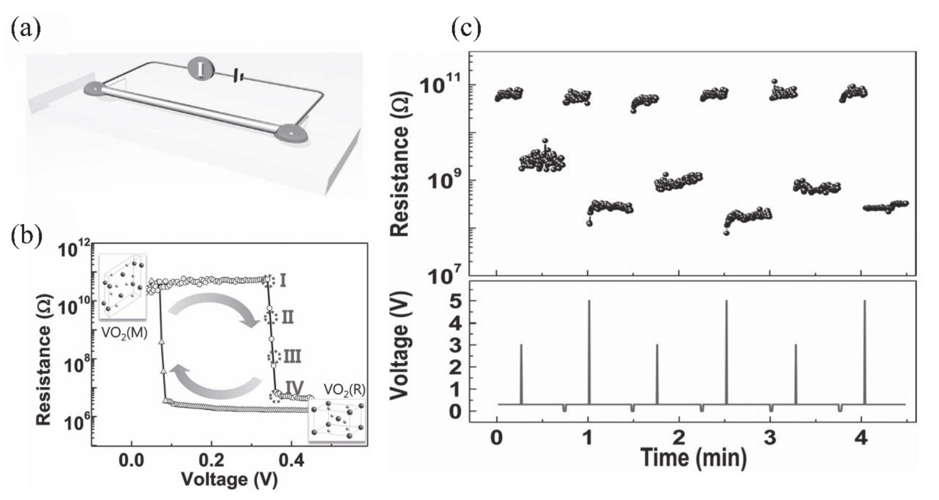
4.1.1. Electronic Switch

The huge change of conductance during MIT is an important property of VO2, which makes it a great potential material for electronic switches [7,125,126,127,128]. Generally, the electronics switches based on VO2 can be driven by temperature or by applying a static current [125] and a static voltage [7,127]. The electronic switch based on VO2 has good performance in speed and broadband operation [125]. The connection and disconnection of the circuit can be controlled by adjusting the metal or insulating phase of VO2 when it is connected in series to the circuit. Most electronic switches are operated based on voltage-driven MIT of VO2. Stefanovich et al. [126] designed a VO2-based electronic switch device and reported that the MIT occurred at a threshold voltage of 2 V. The experimental results demonstrated that the phenomenon of switching no longer occurred when the temperature was higher than Tc. Therefore, temperature plays an important role in VO2 electronic switching. Boriskov et al. [127] studied the I–V characteristics of VO2 switching devices at different temperatures. Different voltages are required to trigger MIT when the ambient temperature is changed. Figure 18a illustrates the cross-sectional diagram of a VO2 two-terminal switching device, and the corresponding electronic switching characteristics of the device are shown in Figure 18b [7]. In addition, Crunteanu et al. [125] studied voltage-mode and current-mode VO2-based switches, as shown in Figure 18c. They demonstrated that current-driven VO2-based switches operated more than 260 million cycles without failure; that is a longer lifetime than in the voltage-driven mode (breakdown at about 16 million cycles). Thus, the integration of VO2 has great potential in device applications with large numbers of stable and repeatable switching cycles. On the other hand, as is known to all, temperature is a facile way to achieve the resistance switching of VO2. Therefore, the corresponding resistance switching is consistent with MIT behavior. As a strongly correlated electron material, the MIT behaviors of VO2 are sensitive to the size and surface effects. In our previous work, the two-terminal switching devices based on single crystalline VO2 (A) NWs with different sizes were reported [20]. Due to the size and surface effects, the hysteresis loops, MIT temperatures and resistance switching of VO2 (A) with different widths showed great differences, as shown in Figure 18d–i. When the width of NWs is less than the critical size, the first-order phase transition even transforms via high-order, continuous phase transition. Therefore, it presents abundant resistance switching states to meet various application requirements.

4.1.2. Field-Effect Transistor (FET)

Field-effect transistors (FETs) are conductive devices based on the early triodes and are controlled by the gate voltage. Compared with triodes, FETs have the advantages of high input impedance, low temperature effect, low noise, low power consumption, high switching speed and low production process difficulty. Among all the FETs, the metal–oxide-semiconductor FET (MOSFET) is one of the most widely used semiconductor devices [129]. MOSFET generates current by carrier diffusion and drift. In recent years, silicon-based FETs have become an essential electronic unit in modern semiconductor technology. However, the inherent size limitation of silicon makes it unsuitable for the manufacture of smaller FET devices. The sub-threshold swing should not be lower than the limit of 60 mV/dec. Otherwise, the power consumption, switching rate and integration of FET devices will be seriously influenced. Therefore, it is an urgent need to find alternatives for silicon materials. MIT materials are considered as promising channel materials for nanoscale FETs. Compared with traditional silicon-based materials, MIT materials have larger changes of carrier concentration during MIT [130,131]. Among the FETs based on MIT materials, VO2-based FETs have been widely studied due to their ultrafast MIT speeds and large changes of carrier concentration. Hormoz et al. [132] demonstrated that the concentrations of free carriers induced by MIT in VO2 are several orders of magnitude larger than those in silicon. Therefore, the VO2-based FET can easily overcome the carrier-transit-time limitation of traditional MOSFET.
Recently, some attempts have been carried out to combine VO2 thin films/NWs with solid-state or ionic liquid (IL) electrolyte gate dielectrics [4,5,6,40,133,134,135,136,137,138]. The SiO2, TiO2, Al2O3/SiO2 and oxide/organic hybrids were usually used as solid-state gate dielectrics [5,133,134,135,136]. For the VO2-based FETs, the controllable MIT behavior plays an important role on the design of electronic devices. Yajima et al. [138] observed a positive-gate-bias-controlled MIT behavior of VO2 near the transition temperature with the high-permittivity TiO2 as gate dielectric. The schematic diagram and corresponding optical images of the device are shown in Figure 19a,b. The n-type Nb-doped titanium dioxide (Nb:TiO2) single crystal was used as the back gate electrode to realize the reverse Schottky gate geometry, as displayed in Figure 19c,d. In this inverse Schottky grid geometry, high permittivity and high breakdown voltage can be achieved in the depleted single-crystal Nb:TiO2 dielectric at the interface. They observed that a large number of electrons were accumulated through the modulation of high-permittivity TiO2 gate (see Figure 19e,f). Besides, Wei et al. [136] reported a VO2-based FET by using high-k oxide Ta2O5/organic parylene-C hybrid as the gate dielectric layer. They found a significant hole–electron asymmetry that is related to the suppression of Tc of VO2. It was proposed that the MIT of VO2 may be induced by the electrostatic field. Based on this, Abbas et al. [5] used Al2O3/SiO2 hybrid gate dielectrics to control the MIT behavior of VO2 at room temperature. The carrier concentration in VO2 devices raises with the increase of gate electrostatic effect. This was attributed to the electronic transition under the electrostatic effect [5]. However, in general, the regulation of solid-state gate cannot achieve the desired results [136,139,140]. It can be attributed to the insufficient quality of gate dielectrics layer and interface between gate and channel, which leads to the poor electric field effect and cannot provide enough electron density accumulation for MIT in VO2 [136].
On the other hand, the IL dielectric gate, which can produce a stronger electric field than the solid-state dielectric gate, has become a popular gate of VO2-based FETs [6,40,137,138]. In electrolyte gating, a high electric field in an electric double layer (EDL) at the interface between electrolyte and channel material can lead to the accumulation of carrier density exceeding 1014 cm−2, which is more than 10 times larger than that of traditional gate modulation [138]. This accumulation of high carrier density allows the induction of electron phase transition in the relevant electronic oxides. Previous works have demonstrated the ILs-gate-induced reversible MIT in VO2 [141], and sometimes there is no electrostatic effect in VO2 except doping [142]. Moreover, once the defects are formed, the MIT should become irreversible [6]. Shibuya and Sawa [138] reported a reversible MIT of VO2, which was achieved by protonation reaction under gate modulation. Figure 19g shows the working process of the VO2 FET based on ILs gate, which is mainly the migration of H+ from ILs between ILs and VO2 channel under ILs gate electric field [138]. With gate-induced protonation, the H+ from ILs migrates into VO2, and the chemical reaction is VO2 + γH+ + γe → HγVO2. After restoration to the pristine state, the chemical reaction is HγVO2 → γH+ + VO2 + γe, and H+ from the VO2 channel migrates into the ILs. As shown in Figure 19h, a reversible MIT of VO2 is demonstrated from the temperature-dependent plate resistance (Rs) in VO2-based ILs FET at different gate voltages. What is more, Jo et al. [143] used solid-state proton electrolyte to achieve a reversible MIT of VO2 at room temperature. A large number of H+ ions were effectively injected into VO2 channel under gate bias voltage without oxygen defects. The H+-induced MIT of VO2 is due to the large modulation of the out-of-plane lattice parameters by the H+-induced chemical expansion.
Moreover, ferroelectrics also are popular dielectric materials in recent years. The ferroelectric materials have excellent properties—a strong polarization response, high-speed switching and a nonvolatile nature. In the ferroelectric gate FET (FeFET), the polarization orientations can be easily tuned by an applied electric filed. Moreover, the remnant polarization in the ferroelectric means the polarization state can be maintained even if the electric field is removed. In recent years, studies on VO2-based FeFET have been reported. The VO2/ferroelectric heterojunctions have been fabricated and different polarization states in ferroelectrics can be tuned through the electric field. Therefore, different strain states are induced at the interface of VO2/ferroelectric and the multi-resistance state of VO2 is realized [144,145,146]. The MIT behavior of VO2 is sensitive to the strain effect so that multi-resistance states are obtained. These properties of VO2 make it have a potential application in strain sensors (detailed in the next section). Zhang et al. [145] reported a VO2/ferroelectric thin film heterostructure device and investigated the piezoelectric control of resistance switching in a VO2 thin film, as the device shown in the inset of Figure 20a. Under the electric field, the piezoelectric effect of ferroelectric thin film introduces the lattice strain at the interface of a VO2/ferroelectric thin film, and leads to the reversible resistance change of VO2. The modulation of electric field at different temperatures shows that the lattice strain at the interface of VO2/ferroelectric will degenerate at a high temperature (close to Tc) (Figure 20a,b). Therefore, a lower temperature is more conducive to the piezoelectric control of resistance switching in VO2. In previous work, the VO2 NW-based FeFET was fabricated based on VO2 NW and a ferroelectric thin film of Pb(Zr0.52Ti0.48)O3 (PZT), with the VO2 NW as a conducting channel and PZT as a gate dielectric layer (Figure 20c) [147]. In this work, the conductance of the VO2 NW channel could be modulated by the ferroelectric gate. The resistance change was up to 85% under the gate voltage of 18 V (electric field of ~0.75 MV cm−1). Moreover, a large resistance change of 50% was still observed even though the system under the zero gate voltage. It was attributed to the remnant polarization in the ferroelectric thin film being also able provide the similar equivalent electric field for the channel of VO2 NW. Additionally, multiple resistive states could be realized when the pulsed gate voltage was applied for the device (Figure 20d–f). This work offers a potential strategy for developing the nonvolatile device based on VO2 FETs.

4.1.3. Memory Device

Generally, an electric field is considered as another effective way to drive MIT behavior, other than temperature. Hysteresis usually exists during the MIT and is usually attributed to the different phase transition paths during the cooling and heating processes. Such a hysteresis is affected by strain, doping and lattice defects during MIT process. VO2 can receive the mismatch strain from the substrate when it is grown on a substrate. Besides, VO2 is often deposited on the substrate in most electronic devices, resulting in a large external strain during MIT. As a result, the hysteresis leads to the metallic phase of VO2 being retained at a relatively low temperature (or applied voltage). Therefore, VO2 can be developed into another potential application in memory devices [12,148,149,150,151]. Combining the advantages of an independent all-oxide cantilever beam and the hysteresis characteristics of VO2, Pellegrino et al. [151] realized a multi-state memory with two-terminal current control. They used VO2/TiO2 free-standing thin film heterostructures via a Joule self-heating process and achieved multistate memory devices nearby the Tc of 70 °C. The memory effect is caused by controlling the formation and growth of metal clusters in the micrometric region by effective Joule heating [152]. In addition, Bae et al. [10] reported a two-terminal memristor memory based on a single VO2 NW at room temperature. Figure 21a shows a schematic of the memristor device with a single VO2 NW, voltage source and ampere meter. Figure 21b demonstrates a distinctive hysteresis loop during the MIT process under the electric field. VO2 stabilized in the insulating phase at a voltage less than ~0.35 V, and MIT was triggered above 0.35 V to reach the metal phase. By contrast, VO2 returned to the insulating phase until the voltage dropped to 0.5 V. Figure 21c displays a demonstration of a VO2-based two-terminal device used for information storage. When the voltage pulse is removed, the NWs maintain low resistance under bias voltage, and zero voltage bias can restore VO2 to its original insulating state. Interestingly, Coy et al. [149] reported the optoelectronic and all-optical multiple memory states in VO2. They measured resistance and near-infrared transmittance of VO2/SiO2 samples in the heating branch of the hysteresis loop at the appropriate temperature. Optical and electrical loads can be effectively combined to get several kinds of reading–writing mode. As long as the appropriate temperature was maintained, these multiple memory states were found to remain stable for at least several hours, and even indefinitely in this case. Moreover, in VO2-based memory devices, a mature chemical doping method or strain effect can be used to adjust the hysteresis gap of VO2 to get a more stable memory effect.

4.2. Optical Devices
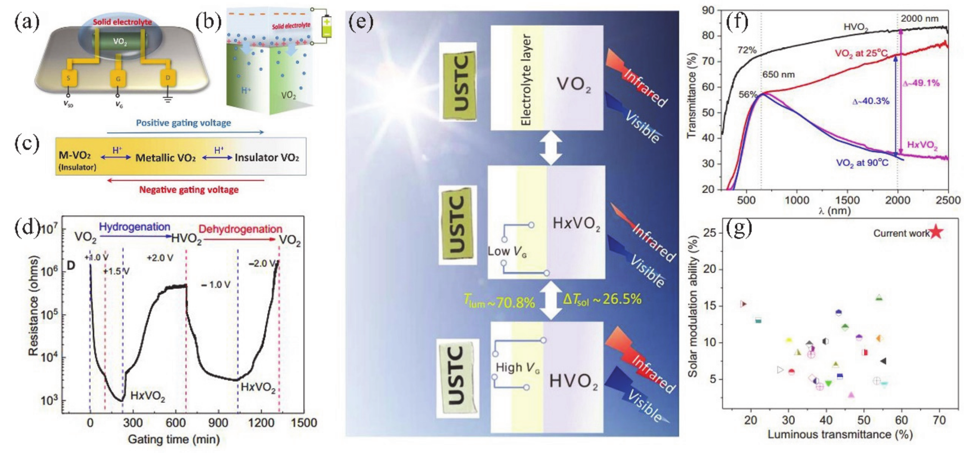
4.2.1. Smart Window

VO2 exhibits a great change in optical performance when MIT occurs. Before MIT, insulating VO2 (M) has high transmittance to infrared light. VO2 (M) changes to VO2 (R) and leads to low infrared transmittance when the temperature rises to the Tc. This unique feature makes it attractive in the application of thermochromic smart windows. Infrared rays can pass through the glass normally at low temperatures. When the temperature is higher than a certain value, the infrared ray is isolated and the indoor temperature remains stable. Although the studies on the VO2-based smart window have been carried out for a long time, it has not yet reached commercial utilization. The practical applications of VO2 smart windows are greatly limited by their unsatisfactory intrinsic properties, e.g., relatively high critical temperature, an unpopular yellow color, poor solar energy regulation ability (∆Tsol) and insufficient luminous transmittance (Tlum). In the past decades, researchers have been trying to solve these problems to achieve VO2 thermochromic windows. Doping is a good means to control the phase transition temperature; doping with high-valence elements of tungsten (W6+) is one of the popular routes to reduce the phase transition with a reduction rate of ≈20–28 K per at% [153]. However, in most cases, reducing Tc by doping leads to the degradation of Tlum and ∆Tsol [154]. Other solutions, including intrinsic structure optimization (e.g., particle size, crystal morphology, and porosity) [155,156] and selection of composite structure (core-shell nanostructure, hybridization, multilayer structure, etc.) [9,157,158,159], can improve VO2 thermochromic properties to a certain extent.
As we know, hydrogen is the smallest and lightest atomic element, which can effectively insert or remove the gap position of VO2, thereby modulating the MIT behavior [143,160]. The research results of Yoon et al. [160] demonstrated that VO2 stabilizes in the metal phase at a low hydrogen concentration, and the hydrogenated insulating phase (note as HVO2 phase) occurs again at a high hydrogen concentration. In the latest study, Chen et al. [11] took full advantage of this particular performance and developed an electrochromic smart window system based on a VO2 film under the solid-state electrolyte gate voltage control at room temperature. Their results broke all previous records with excellent thermochromic performances. Figure 22a–c shows the experimental schemes of gate-induced VO2 channel conductance modulation. The modulation mechanism is similar to the application of the IL gate FET mentioned before. This process shows that VO2 changes from an insulating to metallic state when a low concentration of hydrogen is injected into VO2; the VO2 appears as an insulating phase again and when the concentration of hydrogen increases continuously. Under the gate-controlled effect, the tristate transition of VO2 is realized. These results are in line with the work of Yoon et al. [160]. The gate-controlled VO2 phase transition is a reversible process. The experimental results are shown in Figure 22d. The phase transition of VO2 thin films can be controlled by gate voltage at room temperature, and a diagram of voltage-controlled smart window is displayed in Figure 22e. Obvious color changes are observed with three different phases of VO2 films. Pure VO2 thin films (VO2) and low hydrogen-doped VO2 thin films (HxVO2) have similar yellow colors, while heavily hydrogen-doped VO2 thin films (HVO2) are almost transparent. Figure 22f illustrates the optical transmittance spectra of VO2, HxVO2 and HVO2 thin films. The transmittance of the original VO2 film and metal HxVO2 is about 56% at 650 nm, and that of the insulating HVO2 film is up to 72%. In the infrared region, the transmittance difference of a pure VO2 film at 2000 nm is about 40.3% in the MIT process (the transmittance at 25 °C is higher than that at 90 °C), and the transmittance change from metal HxVO2 film to insulating HVO2 film is 49.1%. Figure 22g shows the comparison of the results of the work of Chen et al. [11] (★) and the previously reported data in terms of light transmittance Tlum and the solar modulation ability ∆Tsol. These performances of their devices break all previous records and exceed the theoretical limit of traditional VO2 smart windows. This indicates that their devices are promising for energy-saving utilization.

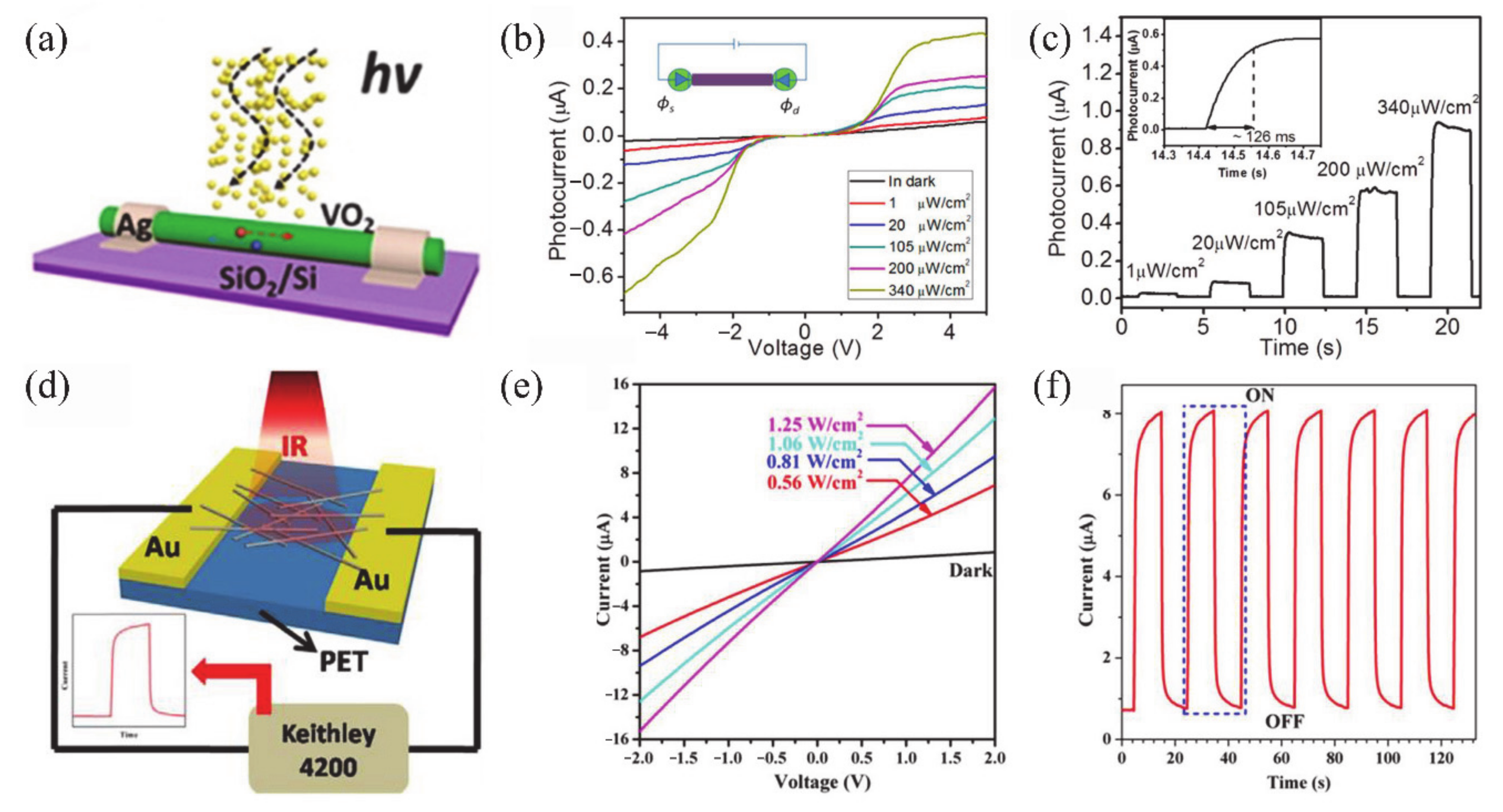
4.2.2. Photodetector

Other than smart windows, the unique optical properties of VO2 during MIT also point to other promising applications in tunable photonic crystals [161], optical switching [162], photodetectors [79,163,164,165] and other optical devices [8,166]. Previous studies have shown that light is a sample way to trigger the MIT behavior of VO2. Lysenko et al. [167] reported that VO2 thin films can be induced to undergo reversible MIT by using a laser (energy density being 7–14 mJ cm−2) as an excitation source. The response of VO2 to light can be used to design the photodetector. Wu et al. [79] fabricated VO2 nanodevices based on photo-induced phase transitions of VO2 NWs under ultraviolet (UV) light at room temperature. Their results demonstrated that the devices exhibited excellent photoresponsive properties. The ratio of photocurrent-to-dark current was 719, and the VO2 NWs possess high electron mobility of 29 cm2V−1S−1 under 2.23 mW cm−2 UV irradiation. Besides, Wu et al. also developed a photodetector based on a single VO2 microwire with ultrahigh responsivity (Rλ) and external quantum efficiency (EQE). The schematic of the device is shown in Figure 23a [163]. The photodetector showed an excellent response for ultraviolet light (λ ≈ 360–400 nm). Figure 23b shows the I–V curves under various light intensities (from 0 to 340 μW cm−2). Under positive and negative bias voltage, the photoelectric current of the photodetector increased with the increase of light intensity. Figure 23c reveals that the photocurrent increased to its equilibrium state immediately when the UV light was turned on. Reversely, the photocurrent fell to its initial state when the UV light was removed, and the corresponding response time was about 126 ms. The responsivity of VO2 photodetector was 6 and 4 orders higher than other those of graphene (or MoS2) and GaS, respectively [168,169,170]. This ultraviolet photodetector with a high response and EQE was the first report of nanomaterials based on a single VO2 microwire.
Furthermore, Li et al. reported the infrared (IR) response of self-heating VO2 NPs by using an Ag NW-based heater [171]. The IR photodetector is an important technology for civil and military use. As a narrow-bandgap semiconductor (0.7 eV) [163], VO2 will be a promising material for IR photodetectors [164,165]. Hou et al. reported an IR photodetector based on a network of as-grown VO2 (M1) NRs [164]. The VO2 (M1) NRs were synthesized by a hydrothermal method with further annealing treatment. Figure 23d illustrates the schematic of the IR photodetector device. The I–V characteristics of the device under different IR light intensity (980 nm) intensities are shown in Figure 23e. Like UV radiation, the photoelectric current of the photodetector increased with the increase of light intensity both on the positive and negative bias voltages. Figure 23f demonstrates a time-dependent photoresponse of the device. The light on and light off periods were both 10 s. Obviously, the device exhibited a “low-current” state in the dark and a “high-current” state under irradiation. The device was used with a high photosensitivity with rising and decay times being 1.6 and 1.0 s, respectively, and an excellent stability of more than 150 cycles at room temperature. Their results indicated that the networks of VO2 (M1) NRs were an ideal strategy for the application of IR photodetector.

4.3. Multi-Responsive Devices

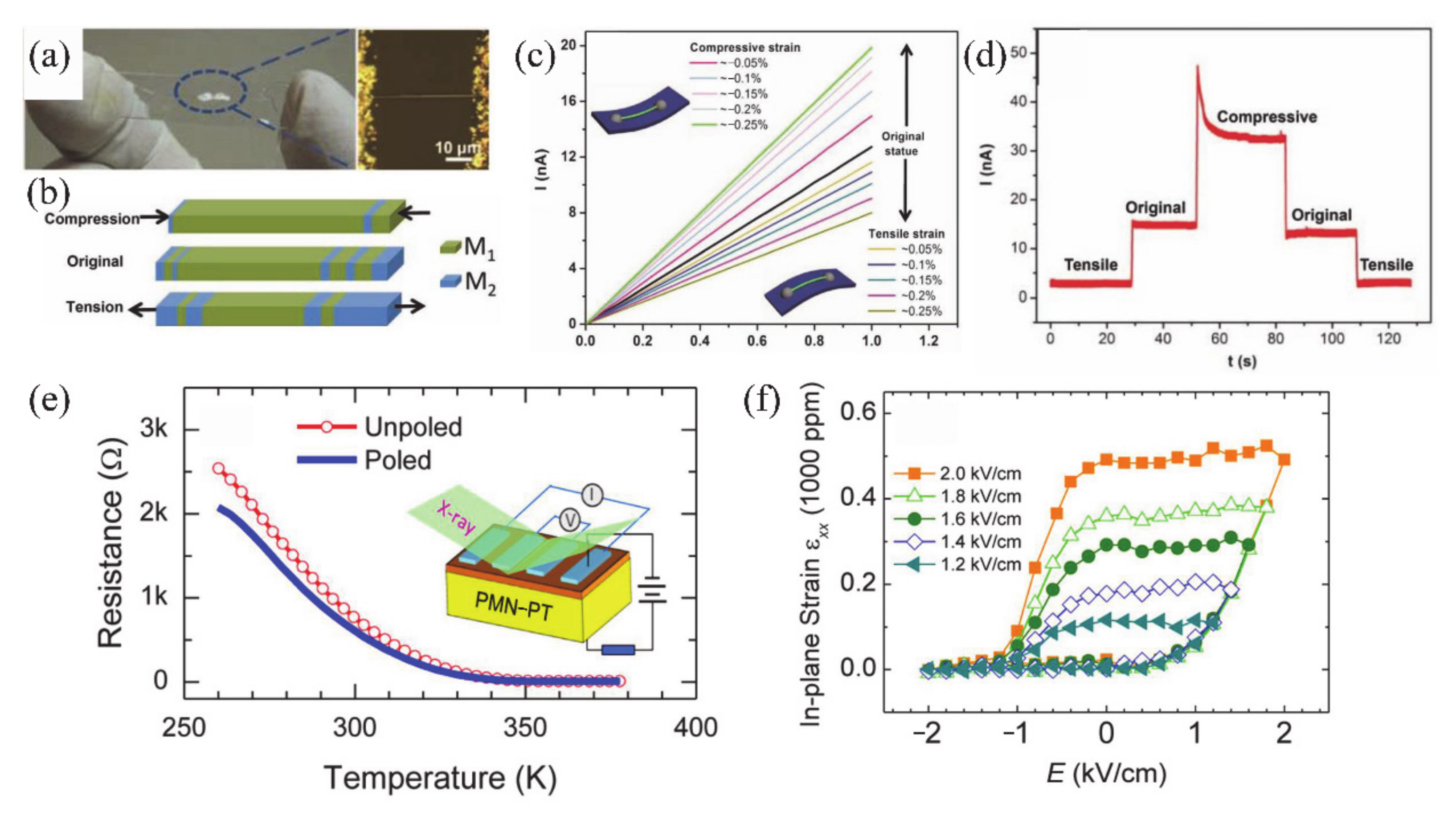
4.3.1. Strain Sensor
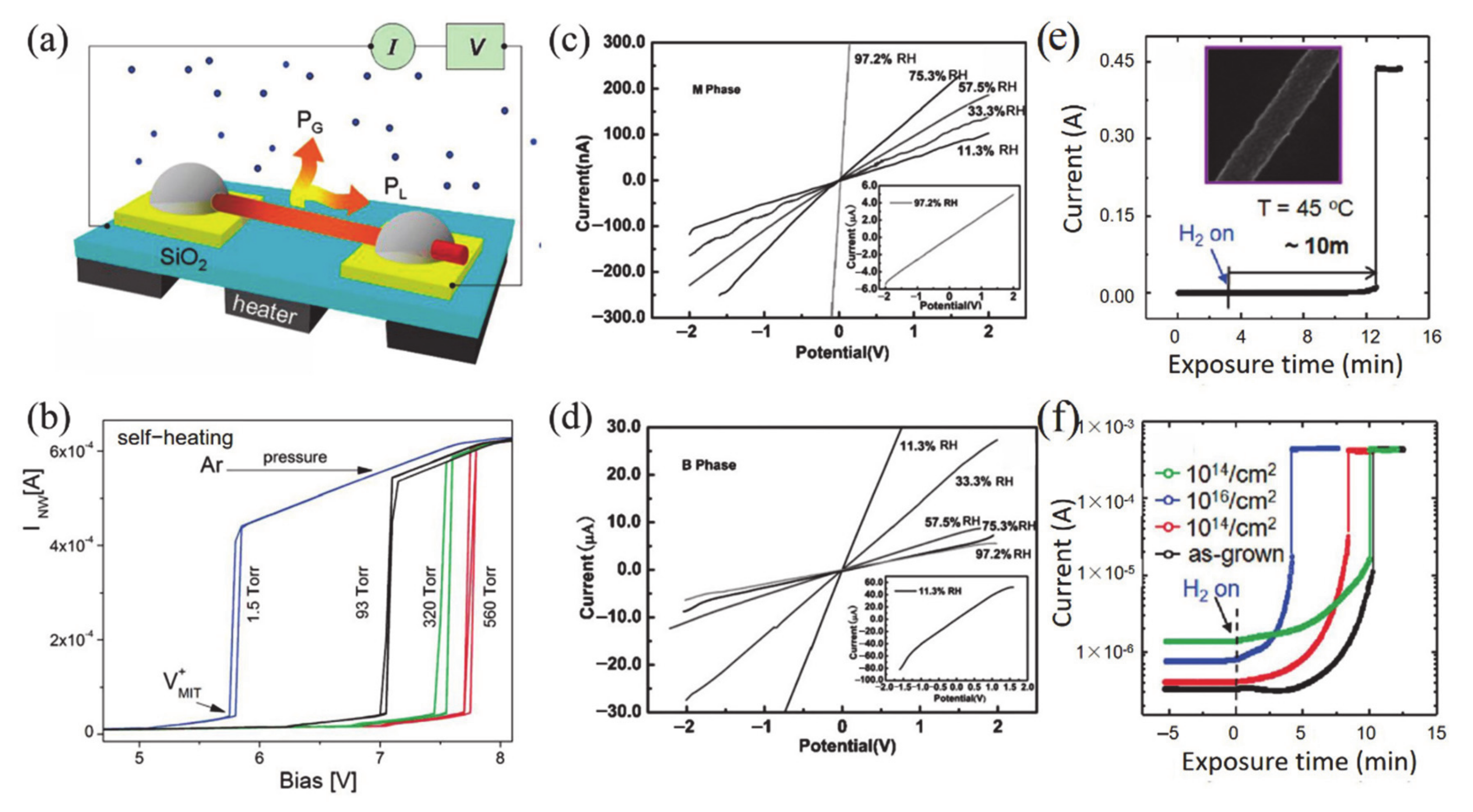
The lattice strain usually has significant effect on the electrical, optical and magnetic properties of materials, especially in strongly correlated electron materials. Due to the strong Coulomb force between electrons, the macroscopic properties of materials exhibit many unique physical phenomena, e.g., quantum phase transition, high-temperature superconductivity, quantum critical phenomena, giant magnetoresistance effect, metal–insulator transition, fractional quantum Hall effect, etc. VO2 has been proved that the MIT temperature, hysteresis loop, conductivity and domain structure are very sensitive to the strain. According to Clausius–Clapeyron formula, the relationship between MIT temperature Tc of VO2 and strain σ can be expressed as follows [12],
d T c d σ = ( ε 0 T c 0 ) / Δ H
Among them, Δ H is the latent heat of phase transformation, T c 0 is the metal–insulator phase transition temperature in the strain-free state (i.e., T c 0 = 341 K) and ε 0 is the expansion of specimen along the c-axis during the phase transition from R phase to M phase (i.e., ε 0 ≈ 1%). Previous results have demonstrated that d T c / d σ is about 1.2 K kbar−1 under the uniaxial stress along c-axis [172]. During the phase transition process of VO2, the volume change of VO2 is much weaker than the expansion of c-axis. Therefore, it can be inferred from the formula that the Tc of VO2 is more sensitive to uniaxial strain than hydrostatic pressure. This provides an effective and efficient approach to modify the MIT temperature and domain structure of VO2 and implies promising applications of VO2 in the strain sensor.
In the strain engineering of VO2, the two main ways for applying uniaxial strain are by lattice mismatch and by applying external axial strain [12,173]. Muraoka and Hiroi reported that the higher mismatch between VO2 and substrate should induce the higher MIT temperature [173]. Previous reports also showed that the MIT temperature of VO2 increases or decreases when applying the uniaxial tensile or compressive stresses along c-axis [173]. Moreover, the strain induced by the lattice mismatch also has a significant effect on the domain structure of VO2, especially for the 1D VO2 NWs. Generally, freestanding VO2 NWs exhibit single domain structure due to the absence of strain effect, while multiple domain structures will appear under the mismatch strain or external strain [12,82,174,175,176]. Hu et al. [175] fabricated a VO2-based strain sensor using the flexible polystyrene (PS) as substrate and studied the external strain effect on the phase transition between M1 and M2 of VO2 nanobeam. Figure 24a shows the fabricated strain sensor and corresponding enlarged image of the bonded nanobeam. Figure 24b illustrates the schematic of M1 and M2 domain configurations under tensile and compressive strains, and the corresponding I–V curves are displayed in Figure 24c. The increase of compressive strain leads to an increase current of VO2, and the increase of tensile strain reduces the current. The results indicate that M1 phase is preferred to appear and more stable under the compressive strain, whereas M2 phase tends to appear under the tensile strain. Furthermore, the response time of the strain sensor device was studied with the bias of 1 V, as shown in Figure 24d. The device exhibits a quick response to the strain switches. The results indicate that this device is suitable to serve as a strain sensor within a small mechanical strain range (±0.25%). Zhi et al. [144] fabricated VO2/PMN-PT (111) heterostructures and investigated the non-volatile switching modulation by ferroelectric polarization strain. The polarization strain of ferroelectric PMN-PT layer was induced by the electric field, leading to an effective resistance switching of VO2 between low and high resistance states. Figure 24e demonstrates the temperature-dependent resistance curves of VO2 film under the two polarization states (unpolarized high resistance state and polarized low resistance state). Based on the different polarization states of PMN-PT, multiple resistance states can be achieved by applying electric fields across the heterostructures appropriately (Figure 24f). More importantly, the resistance can keep unchanged after withdrawing the electric fields because of the non-volatility of ferroelectric PMN-PT layer. This provides another strategy for the application of VO2-based strain sensor. In addition, Chen et al. [177] mapped the pressure-temperature phase diagram of VO2 nanobeams under different hydrostatic pressure. Their research showed that pressure led to different phase transition temperatures of VO2. By combining the experiment data of optical reflectance, Raman, and electrical transport performance, they obtained the pressure-temperature phase diagram of VO2. The phases include M1 (I), M1′ (I), R (M), O (M) and X (M), where I and M represent insulating and metallic phases of VO2, respectively. Under the low temperature (<60 °C) and low pressure (15–20 GPa) conditions, VO2 is stabilized in M1 phase. Meanwhile, VO2 can maintain the metallic phase under high pressure (about 40 GPa). Their results indicate that VO2 can be used to develop an excellent pressure sensor.

4.3.2. Gas Sensor

A transition edge sensor (TES) composed of phase change materials is an effective method to detect gas atoms under ambient conditions. Strelcov et al. [13] fabricated a VO2 NW-based Ar gas sensor model (Figure 25a). By changing the temperature of NWs near the edge of phase transition, the conductance of NWs becomes very sensitive to small changes of the surrounding gas environment, e.g., the molecules, pressure, temperature and humidity. Therefore, VO2 exhibits different phase transition behaviors in such ambient atmospheres. They found that the increase of Ar pressure led to the decrease of heat dissipation of VO2 NW, and resulted in the increase of phase transition voltage, as shown in Figure 25b. Their results open up new opportunities for VO2-based gas sensors. Sensors for different kinds of gases have been developed, e.g., steam (humidity sensing) [178], hydrogen [179,180], carbon monoxide and carbon dioxide [180]. Yin et al. [178] fabricated two humidity sensors based on VO2 (B) and VO2 (M) nanoflowers with large surface-to-volume ratios and sensitive humidity sensing performances. The I–V curve of VO2 (M) nanoflower film-based resistive-type sensors under different static air relative humidity of 11.3–97.2% at room temperature is shown in Figure 25c. With the increase of relative humidity, the current of VO2 (M) slowly rises. The current changes up to about an order of magnitude when the relative humidity reaches 97.2%. In contrast, the conductivity of the VO2 (B) nanoflower film changed conversely with the increase of relative humidity (Figure 25d). The resistance of VO2 returned to its original state when the sensor was out of the humid environment. Most importantly, the VO2 (M) sensor is more sensitive in a high relative humidity, whereas the VO2 (B) sensor is more sensitive in low relative humidity. Therefore, the VO2 nanoflowers with large surface-to-volume ratios are good candidates for developing humidity sensors.
On the other hand, a hydrogen sensor is an important research topic. Byon et al. [179] developed a highly responsive and selective hydrogen sensor based on MIT of Pd-decorated VO2 NWs. The conductivity of VO2 has a significant four-times increase when under the irradiation of an electron beam, while the temperature of MIT varies moderately. Figure 25e shows the current in the as-grown Pd-decorated VO2 NW as a function of hydrogen exposure time under a bias voltage of 10 V and a temperature of 45 °C. The current evolution can be divided into two stages. In stage I, the current of VO2 NW increases slowly with the exposure time of hydrogen. This slow process takes place in a few minutes and depends on electrical conductivity and ambient temperature. In stage II, the current of NW increases about 1000-fold after exposing in hydrogen about 10 min. This ultra-fast process takes several nanoseconds or microseconds to reach the metal phase. The slow process is considered as a complex process, which may involve the formation of hydrogen atoms, the interaction with Pt, the migration of hydrogen atoms to the surfaces of oxides and the infiltration into the volume region of oxides, etc. In the second ultra-fast process, the hydrogen matrix acts as an electron donor and increases the carrier density in the conduction band, so that the conductivity of VO2 has a significant increase. Figure 25f shows the evolution of current with exposure time of Pd-modified VO2 NWs under different irradiation conditions (i.e., energy and dose). It is obvious that VO2 undergoes different MIT behaviors with the change of electron beam irradiation conditions when it is exposed to hydrogen. Obviously, the response time is significantly reduced to less than 4 min when it increases the dose up to 1016/cm2, and only half of the time without irradiation (~10 min). The increase of conductivity induced by irradiation accelerates the self-heating effect and leads to the decrease of response time, working temperature and voltage. Moreover, the sensor also shows the ability to selectively detect hydrogen in gases (oxygen, carbon monoxide and ethylene).

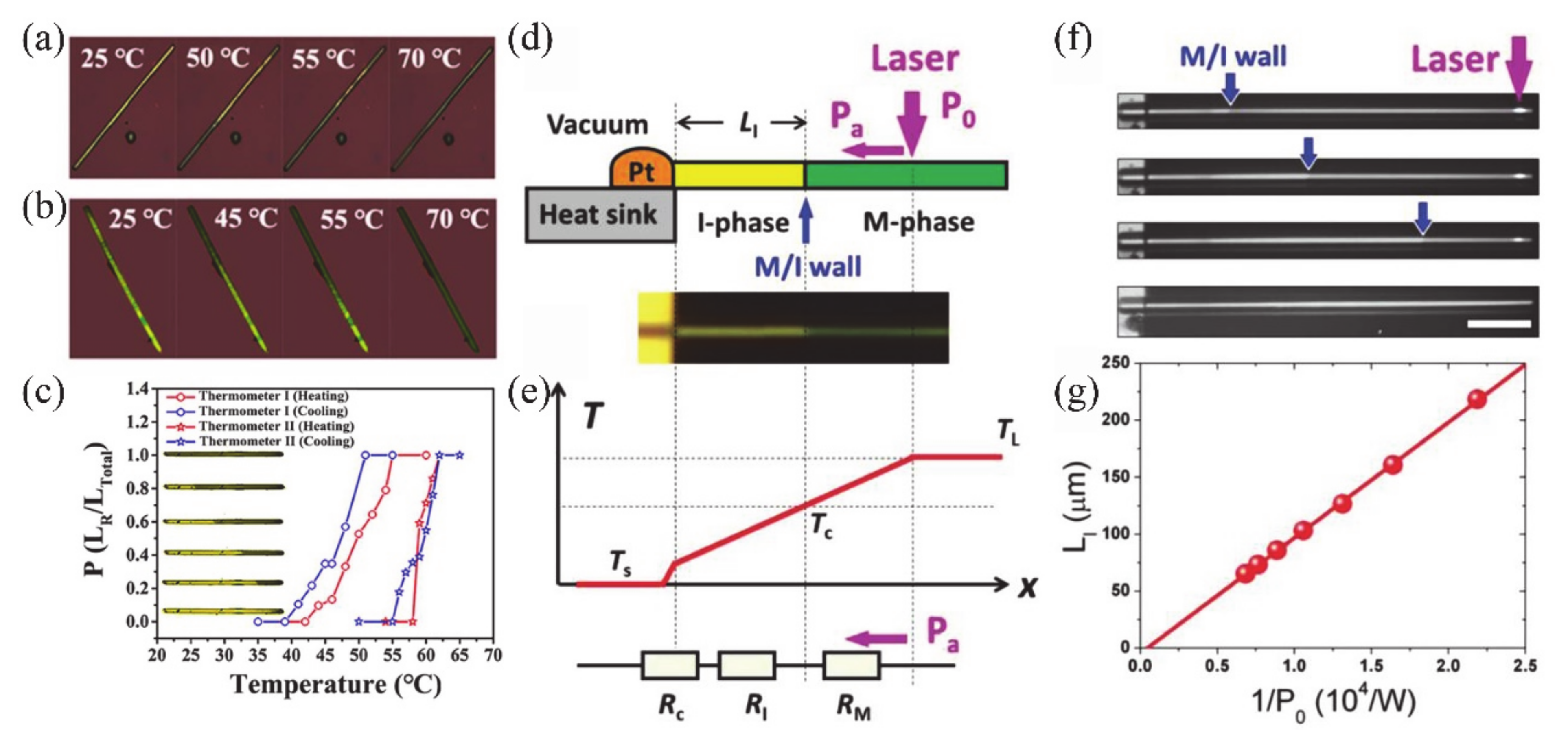
4.3.3. Thermal and Laser Sensors
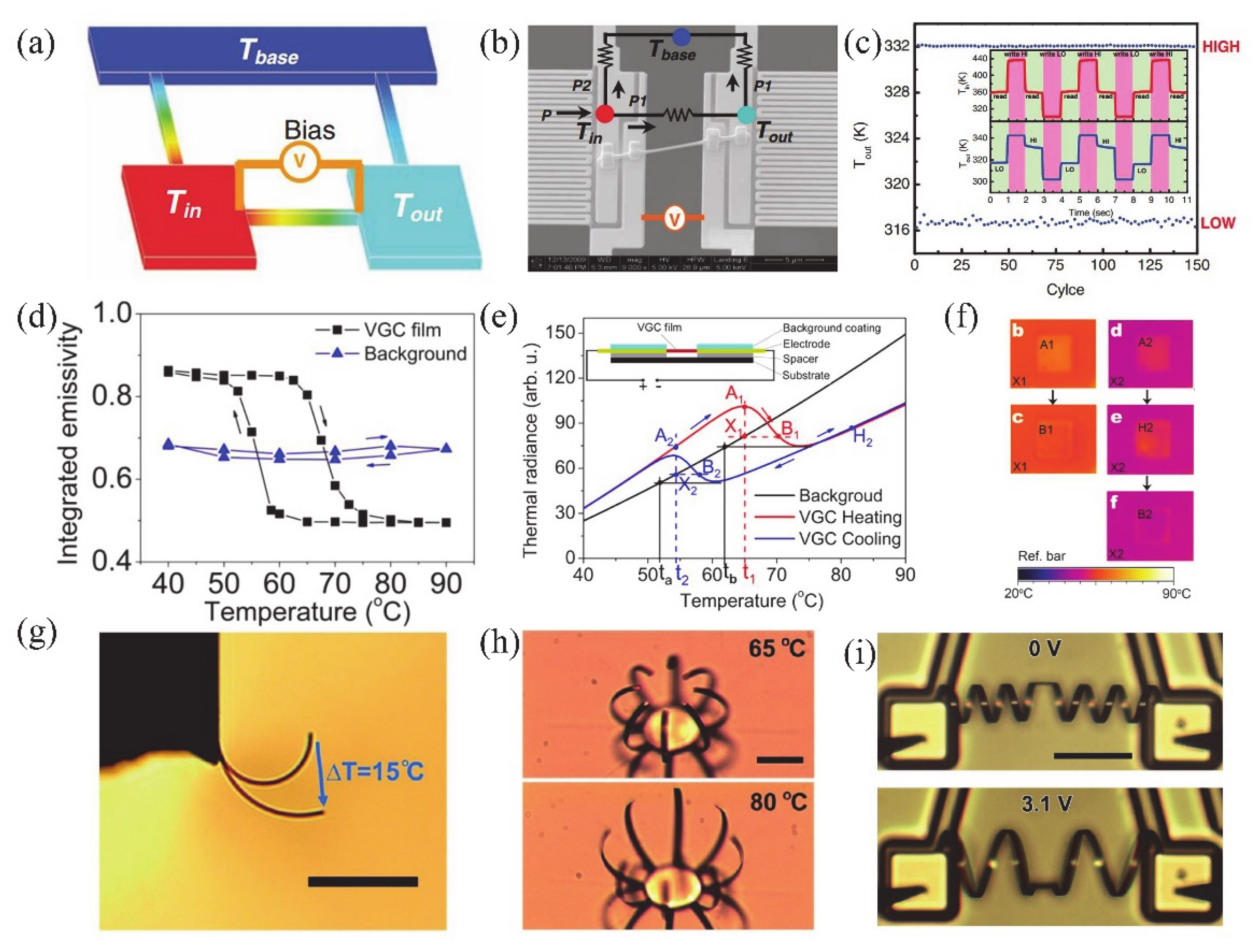
With the rapid development of nanotechnology, it is urgent to develop more accurate and quantitative measurement technology on nanostructures. So far, powerful solutions for in situ and local temperature measurements of micro-nanoobjects remain limited. We know that VO2 is very sensitive to temperature, and MIT behavior occurs under certain temperature conditions. VO2 nanostructures (NWs, NSs) usually exhibit a single M domain structure under optical microscopy without external stimuli. When they are exposed to external stimuli, such as strain and heat, VO2 NWs exhibit distinct M–R domains until they are completely converted to R domains [12,82,176]. Therefore, aside from the strain sensing mentioned above, thermal sensing is also a typical application of VO2. Shi et al. [181] took advantage of the properties of thermal sensing and developed optically readable thermometers based on graded H-doping NWs. Figure 26a,b shows the evolution of M–R domains during heating process. It is obvious that M domain decreases and R domain increases with the raising of temperature. Moreover, the length of the metal domain of NWs rises linearly with the increase of ambient temperature. (Figure 26c). It is noteworthy that the NW-based thermometer can move in the heating and cooling processes outside the hysteresis-free domain; thus, sensitive real-time temperature monitoring is realized, and an excellent performance via good relative sensitivity (17.4%/K) and temperature resolution (0.026 K) is achieved. However, there are still some challenges in its practical application. For instance, the modulation range of MIT temperature is limited. Therefore, more research is needed to develop VO2-based thermal sensors.
Another interesting application based on VO2 NWs is about the effect of laser on the M–R domain wall of VO2 movement. Laser heating can also induce the MIT behavior of VO2 [183]. This property can be exploited to develop a novel VO2-based laser power meter. Cheng et al. [182] demonstrated a multifunctional power meter based on VO2 NWs, and the light absorption and heat transfer directly can be quantified in the near field length range (Figure 26d–g). The laser struck on the one end of the NW, and the laser power flowed unidirectionally toward the substrate. Once enough power is obtained, the metal domain appears, and the temperature of the domain wall just turns into 68 °C. In fact, the length of the insulating domain (LI) decreases with the increasing of the laser power (P0), which corresponds to the domain distribution of VO2 NW at different temperatures. By changing the optical power (laser or electron beam), the optical absorptivity of VO2 NWs can be determined from the slope of LI − 1/P0. These near field power meter can be used for the quantitative study of thermal and optical fields in nanoscale.

4.4. Other Devices

In addition to the above well-known applications, the MIT of VO2 is also related to other aspects. We mentioned earlier that the voltage can drive the MIT of VO2 with an appearance of hysteresis, which implies a potential application in electrical memory devices. It is interesting to note that the hysteresis caused by thermally driven phase transitions can also be used to store thermal information. Xie et al. [184] demonstrated a thermal memory device based on VO2 nanobeams. This device can be used for storing and retaining thermal information, and the temperature states are used as input and output. The thermal memory device includes an input (Tin), an output (Tout) and one heat conduction channel that bridges the two terminals together. Two terminals are connected and then connected to a substrate (Tbase), as shown in Figure 27a,b. VO2 nanobeam was used as a controllable thermal channel to realize the response between Tin and Tout, as shown in Figure 27c. The results prove that the characteristics of thermal memory can be modulated by changing the voltage. To determine the switching performance and repeatability of thermal memory, they used heating and cooling pulses to perform repeated high-read–write–low-read cycles. Repeated cycles of more than 150 times shows that both high and low states were reliable, reproducible and non-degenerative.
The excellent thermal emissivity and large negative differential thermal emissivity of VO2 make it a candidate material for infrared camouflage and thermal regulation [185]. Xiao et al. [186] fabricated VO2/graphene/carbon nanotube (VGC) flexible films with an adjustable emissivity, as shown in Figure 27d. The thermal emissivity of the VGC films is ~0.86 at 40 °C and ~0.49 at 90 °C. The large adjustability of emissivity indicates that the VGC film is a promising active thermal camouflage material. Near the Tc, the thermal radiation of VGC thin films is greatly reduced during the heating process; on the contrary, it increases when cooling. Although the temperature of VGC film is slightly higher than that of background (Figure 27e), its total thermal radiation is almost constant. Therefore, infrared cameras cannot distinguish them, and the process can be easily controlled by electronic adjustment. This infrared camouflage can be used at room temperature by doping to reduce the Tc of VO2.
In addition to reversible changes in resistivity and light transmittance, the reversible strain will also occur during the process of MIT. When VO2 lattice changes from monoclinic (insulating) to rutile (metal) structure, VO2 shrinks under a strain of ε ≈ 1% along the c-axis of the rutile phase and expands in other two directions [12]. Such an abrupt strain of 1% makes VO2 a good active layer for an actuator. Rúa et al. [187] developed a thermally activated actuator based on cantilever bending of polycrystalline VO2 coating. The VO2 thin film was deposited on a silicon microcantilever. The fabricated bimorph cantilever exhibited thermally-driven bending during MIT. The curvature change and amplitude were ~2000 m−1 and ~115 μm, respectively. This is much better than the traditional bimorph actuator based on differential thermal expansion. Besides, in recent years, a series of Cr/VO2 thin film bimorph drivers with different patterns and structures have been reported [188,189,190,191]. Liu et al. developed micro-fabrication steps to design various shapes and structures of micro-Cr/VO2 thin film-based actuators (Figure 27g–i) [188,189]. These actuators can be triggered by different types of stimuli, e.g., heating, electric field, strain and light. The actuators had a high bending amplitude and the actuation frequency was up to ~6 kHz [188]. Besides, Cr/VO2 thin film actuators were further made into coils, which can provide up to 200,000 rpm of torsional motion. The peak power density reached 39 kW/kg, and the measurement of one million driving cycles indicated that the material has strong fatigue resistance. This miniature bending and twisting machine may become a key component of robots, artificial muscles, intelligent shutters and biochemical drug delivery. Ma et al. [190] deposited VO2 on carbon nanotubes (CNT) and realized flexible actuators. By using W-doping technology to reduce the Tc of VO2, these VO2/CNT flexible actuators can work under the stimuli of sunlight or human body temperature.

4.5. Summary

In this section, the properties and related applications of VO2 were introduced. Almost all the application prospects are based on the phase transition characteristic of VO2. The electrical changes caused by MIT make VO2 promising in applications such as electronic switches, FET and memory devices. Due to the change of optical properties caused by MIT and the electrical properties of VO2 being sensitive to light, VO2 can be used to develop smart windows, photodetectors, etc. The MIT of VO2 is sensitive to strain, temperature and surrounding gas environment, which makes VO2 as a candidate material in multiple types of response sensors. The strain produced by the MIT of VO2 makes it useful for micro or nanoactuators. Moreover, VO2 has great potential for developing infrared camouflage and thermal regulation.

5. Summary and Outlook

In this review, we first introduced several phases of VO2, including monoclinic VO2 (M), tetragonal VO2 (R) and metastable VO2 (A), VO2 (B) and VO2 (C); and new phases of VO2 (D) and VO2 (P). Under certain conditions, these phases can be transformed into each other. Among them, both VO2 (A) and VO2 (M) exhibit typical MIT behavior, and VO2 (M) is widely focused on because its Tc is close to room temperature. Then the preparation strategies of VO2 nanostructures are discussed in the second section. The fabrication of the thin films and various LDSs (e.g., NPs, NWs, NRs, NSs, NBs, NDs, nanorings, microspheres and micro- or nano-plates) of VO2 via hydrothermal method, CVD, PLD, sol–gel method, magnetron sputtering, electrospinning and MBE was comprehensively summarized. The hydrothermal method and CVD are mainly used to prepare LDSs of VO2. Such chemical synthesis processes easily produce by-products, such as metastable phases or non-stoichiometric amounts of VO2. Therefore, it is very important to strictly control the synthesis conditions. PLD, magnetron sputtering, MBE and sol–gel are commonly used to grow VO2 thin films. Interestingly, by precisely controlling the deposition conditions, PLD also can fabricate various LDSs. Finally, we discussed the performance and corresponding device applications of VO2, including electrical and optical devices, various sensor devices (e.g., strain sensor, gas sensor, thermal sensor and laser sensor) and other applications (e.g., thermal memory, thermal camouflage and actuators). These show that VO2 has great potential applications in advanced multifunctional devices.
As mentioned above, a series of remarkable breakthroughs in the fabrication of VO2 have been achieved, and many advanced applications have been widely studied. However, there are still some challenges that should be addressed, some of which follow:
(1)
Regarding the fabrication aspect, it is still a challenge to precisely control the sizes and alignments of VO2 products. The size of NWs can directly affect the MIT behavior of VO2; thus, it is important to accurately control the size of NWs. For the hydrothermal method, it is also a tough task to fabricate ultra-small size (<20 nm) VO2 nanostructures. As we mentioned earlier, the decomposition rate of the precursor (rd) and the growth rate of the grain (rg) are two important factors determining the particle size of VO2. Therefore, in the hydrothermal method, VO2 nanostructures with ideal size can be synthesized by controlling rd and rg. Besides, due to the polymorphs of VO2 and the complicated growth process, it is still a challenge to synthesize the VO2 (M) in one step via hydrothermal method. Therefore, the one-step synthesis of VO2 (M) needs to be further explored, and the choice of surfactant or catalyst and the precise control of the synthesis process can be considered in the process of hydrothermal synthesis. For the CVD method, it is a challenge to control the orderly alignment of VO2 NWs. As we mentioned before, one of the strategies to control the growth orientation of VO2 NW is to form a template by modifying the surface structures of the substrate or depositing a patterned seed layer. Meanwhile, catalysts also may be necessary to promote the growth of aligned VO2 NWs. On the other hand, for the PLD, magnetron sputtering and MBE, proper substrate and deposition conditions are key factors for the fabrication of VO2 thin films of high-quality. Besides, surface pre-treatment always is needed to improve the surface status of the substrate and thereby decrease the defects in as-grown thin films.
(2)
For the application aspect, almost all the application prospects are based on the phase transition characteristic of VO2. Therefore, controlling the MIT temperature of VO2 is very important in the device applications. However, the phase transition temperature of VO2 is about 68 °C, which is still too high for applications in electronic devices. In particular, for the VO2-based switch devices, smart windows, laser power meters, thermally activated actuators, etc., the relatively high Tc results in high energy consumption and damage to the device. At present, the conventional approach to control the Tc is doping, and the Tc can be reduced to near room temperature. However, the corresponding slow transition rate and large hysteresis window during the MIT will limit the high-speed responses of VO2-based devices. Therefore, to find an efficient way to tune Tc without affecting the transition rate and hysteresis window of MIT is very necessary to improve the performances of VO2-based devices. On the other hand, due to the intrinsic properties of VO2, e.g., the low resistance of insulating phase in doped VO2, the low visible light transmittance of VO2 smart windows, etc., there is a big gap to realize the practical applications of VO2-based devices. Therefore, in order to improve the performance of VO2-based devices, a good strategy is to combine VO2 with other functional materials (ferroelectric multifunctional layer, etc.) to form composite structures.
(3)
In recent years, phase separation and coexistence (i.e., metal–insulator domain structures) of VO2 became a hot topic due to its importance in the deep understanding of the mechanism of phase transition and the controllability of phase transition behavior. More recently, we found that a macroscopic defect, i.e., a void, has significant influence over the metal–insulator domain structures and their evolutionary paths during the phase transition. By analyzing the distribution of stress field near the defect and the evolution paths of domain structures, we suppose that the defect-induced local stress should play an important role. Defect-induced local stress concentration leads to the pinning of the phases and high agreement in the evolutionary paths of domain structures during the phase transition. Moreover, the shape, position and number of macroscopic defects, which are determinants of the distribution of the stress fields in the VO2 nanostructures, could be precisely controlled by employing a focused ion beam (FIB) and nanoindentation. This results in the MIT temperature, hysteresis loop, conductivity and domain structure of VO2 nanostructures also being precisely controlled. This provides a novel strategy to precisely control the phase transition temperature and behaviors.
Nowadays, with the development of fabrication and micromachining technologies, the above problems are attracting much attention and are gradually being taken on. The improved MIT and multi-functional properties will promote the practical applications of VO2-based functional devices. Besides, numerous new application concepts based on VO2 also have been proposed—e.g., an ultrafast response flexible breath sensor [192], artificial skin [193] and artificial synapses [194]. The emergence of new concepts is expected to expand the applications of VO2 and to acquire more opportunities.

Author Contributions

Y.Z. (Yanqing Zhang): writing of the manuscript and visualization; W.X.: conceptualization, writing, reviewing and correcting of the manuscript; W.C.: reviewing and correcting of the manuscript; Y.Z. (Yue Zheng): reviewing and correcting of the manuscript. All authors have read and agreed to the published version of the manuscript.

Funding

This work was supported by the National Natural Science Foundation of China (grants 12072380, 11702335, 11672339 and 11972382 to W.X., W.C. and Y.Z. (Yue Zheng)).

Institutional Review Board Statement

Not applicable.

Informed Consent Statement

Not applicable.

Data Availability Statement

No new data were created or analyzed in this study. Data sharing is not applicable to this article.

Conflicts of Interest

The authors declare that they have no known competing financial interests or personal relationships that could have appeared to influence the work reported in this paper.

References

  1. Morin, F.J. Oxides which show a metal-to-insulator transition at the neel temperature. Phys. Rev. Lett. 1959, 3, 1. [Google Scholar] [CrossRef]
  2. Gonçalves, A.R.J.; Marques, A.C.; Pinto, J.V.; Nunes, D.; Marie, A.; Goncalves, R.; Pereira, L.; Martins, R.; Fortunato, E. Smart optically active VO2 nanostructured layers applied in roof-type ceramic tiles for energy dfficiency. Sol. Energy Mater. Sol. C 2016, 150, 1–9. [Google Scholar] [CrossRef]
  3. Yang, Z.; Ko, C.; Ramanathan, S. Oxide electronics utilizing ultrafast metal-insulator transitions. Ann. Rev. Mater. Res. 2011, 41, 337–367. [Google Scholar] [CrossRef]
  4. Sasaki, T.; Ueda, H.; Kanki, T.; Tanaka, H. Electrochemical gating-induced reversible and drastic resistance switching in VO2 nanowires. Sci. Rep. 2015, 5, 17080. [Google Scholar] [CrossRef] [PubMed] [Green Version]
  5. Abbas, K.; Hwang, J.; Bae, G.; Choi, H.; Kang, D.J. Control of multilevel resistance in vanadium dioxide by electric field using hybrid dielectrics. ACS Appl. Mater. Interfaces 2017, 9, 13571–13576. [Google Scholar] [CrossRef] [PubMed]
  6. Jeong, J.A.N.; Graf, T.; Schladt, T.D.; Samant, M.G.; Parkin, S.S.P. Suppression of metal-insulator transition in VO2 by electric field–induced oxygen vacancy formation. Science 2013, 339, 1402–1405. [Google Scholar] [CrossRef]
  7. Chae, B.-G.; Kim, H.-T.; Youn, D.-H.; Kang, K.-Y. Abrupt metal-insulator transition observed in VO2 thin films induced by a switchig voltage pulse. Physica B 2005, 369, 76–80. [Google Scholar] [CrossRef] [Green Version]
  8. Zhu, Z.; Evans, P.G.; Haglund, R.F., Jr.; Valentine, J.G. Dynamically reconfigurable metadevice employing nanostructured phase-change materials. Nano Lett. 2017, 17, 4881–4885. [Google Scholar] [CrossRef]
  9. Kim, H.; Kim, Y.; Kim, K.S.; Jeong, H.Y.; Jang, A.-R.; Han, S.H.; Yoon, D.H.; Suh, K.S.; Shin, H.S.; Kim, T.Y.; et al. Flexible thermochromic window based on hybridized VO2/graphene. ACS Nano 2013, 7, 5769–5776. [Google Scholar] [CrossRef]
  10. Bae, S.H.; Lee, S.; Koo, H.; Lin, L.; Jo, B.H.; Park, C.; Wang, Z.L. The memristive properties of a single VO2 nanowire with switching controlled by self-heating. Adv. Mater. 2013, 25, 5098–5103. [Google Scholar] [CrossRef]
  11. Chen, S.; Wang, Z.; Ren, H.; Chen, Y.; Yan, W.; Wang, C.; Li, B.; Jiang, J.; Zou, C. Gate-controlled VO2 phase transition for high-performance smart windows. Sci. Adv. 2019, 5, eaav6815. [Google Scholar] [CrossRef] [PubMed] [Green Version]
  12. Cao, J.; Ertekin, E.; Srinivasan, V.; Fan, W.; Huang, S.; Zheng, H.; Yim, J.W.; Khanal, D.R.; Ogletree, D.F.; Grossman, J.C.; et al. Strain engineering and one-dimensional organization of metal-insulator domains in single-crystal vanadium dioxide beams. Nat. Nanotechnol. 2009, 4, 732–737. [Google Scholar] [CrossRef] [PubMed]
  13. Strelcov, E.; Lilach, Y.; Kolmakov, A. Gas sensor based on metal-insulator transition in VO2 nanowire thermistor. Nano Lett. 2009, 9, 2322–2326. [Google Scholar] [CrossRef]
  14. Strelcov, E.; Tselev, A.; Ivanov, I.; Budai, J.D.; Zhang, J.; Tischler, J.Z.; Kravchenko, I.; Kalinin, S.V.; Kolmakov, A. Doping-based stabilization of the M2 phase in free-standing VO2 nanostructures at room temperature. Nano Lett. 2012, 12, 6198–6205. [Google Scholar] [CrossRef] [PubMed]
  15. Ji, C.; Wu, Z.; Wu, X.; Wang, J.; Liu, X.; Gou, J.; Zhou, H.; Yao, W.; Jiang, Y. Terahertz transmittance and metal-insulator phase transition properties of M2 phase VO2 films induced by Cr doping. Appl. Surf. Sci. 2018, 455, 622–628. [Google Scholar] [CrossRef]
  16. Xiong, W.M.; Shao, J.; Zhang, Y.Q.; Chen, Y.; Zhang, X.Y.; Chen, W.J.; Zheng, Y. Morphology-controlled epitaxial vanadium dioxide low-dimensional structures: The delicate effects on the phase transition behaviors. Phys. Chem. Chem. Phys. 2018, 20, 14339–14347. [Google Scholar] [CrossRef]
  17. Sharma, Y.; Balachandran, J.; Sohn, C.; Krogel, J.T.; Ganesh, P.; Collins, L.; Ievlev, A.V.; Li, Q.; Gao, X.; Balke, N.; et al. Nanoscale control of oxygen defects and metal-insulator transition in epitaxial vanadium dioxides. ACS Nano 2018, 12, 7159–7166. [Google Scholar] [CrossRef]
  18. Wang, X.; Gao, H. Distinguishing the photothermal and photoinjection effects in vanadium dioxide nanowires. Nano Lett. 2015, 15, 7037–7042. [Google Scholar] [CrossRef]
  19. Zhang, Z.; Guo, H.; Ding, W.; Zhang, B.; Lu, Y.; Ke, X.; Liu, W.; Chen, F.; Sui, M. Nanoscale engineering in VO2 nanowires via direct electron writing process. Nano Lett. 2017, 17, 851–855. [Google Scholar] [CrossRef]
  20. Wang, C.Q.; Shao, J.; Liu, X.L.; Chen, Y.; Xiong, W.M.; Zhang, X.Y.; Zheng, Y. Phase transition characteristics in the conductivity of VO2(A) nanowires: Size and surface effects. Phys. Chem. Chem. Phys. 2016, 18, 10262. [Google Scholar] [CrossRef]
  21. Li, W.; Ji, S.; Li, Y.; Huang, A.; Luo, H.; Jin, P. Synthesis of VO2 nanoparticles by a hydrothermal-assisted homogeneous precipitation approach for thermochromic applications. RSC Adv. 2014, 4, 13026–13033. [Google Scholar] [CrossRef]
  22. Cao, C.; Gao, Y.; Luo, H. Pure single-crystal rutile vanadium dioxide powders: Synthesis, mechanism and phase-transformation property. J. Phys. Chem. C 2008, 112, 18810–18814. [Google Scholar] [CrossRef]
  23. Yin, H.; Luo, M.; Yu, K.; Gao, Y.; Huang, R.; Zhang, Z.; Zeng, M.; Cao, C.; Zhu, Z. Fabrication and temperature-dependent field-emission properties of bundlelike VO2 nanostructures. ACS Appl. Mater. Interfaces 2011, 3, 2057–2062. [Google Scholar] [CrossRef] [PubMed]
  24. Popuri, S.R.; Miclau, M.; Artemenko, A.; Labrugere, C.; Villesuzanne, A.; Pollet, M. Rapid hydrothermal synthesis of VO2 (B) and its conversion to thermochromic VO2 (M1). Inorg. Chem. 2013, 52, 4780–4785. [Google Scholar] [CrossRef]
  25. Liu, L.; Cao, F.; Yao, T.; Xu, Y.; Zhou, M.; Qu, B.; Pan, B.; Wu, C.; Wei, S.; Xie, Y. New-phase VO2 micro/nanostructures: Investigation of phase transformation and magnetic property. New J. Chem. 2012, 36, 619–625. [Google Scholar] [CrossRef]
  26. Wu, C.; Hu, Z.; Wang, W.; Zhang, M.; Yang, J.; Xie, Y. Synthetic paramontroseite VO2 with good aqueous lithium-ion battery performance. Chem. Commun. 2008, 33, 3891–3893. [Google Scholar] [CrossRef]
  27. Oka, Y.; Sato, S.; Yao, T.; Yamamoto, N. Crystal structures and transition mechanism of VO2 (A). J. Solid State Chem. 1998, 141, 594–598. [Google Scholar] [CrossRef]
  28. Hagrman, D.; Zubieta, J.; Warren, C.J.; Meyer, L.M.; Treacy, M.M.J.; Haushalter, R.C. A new polymorph of VO2 prepared by soft chemical methods. J. Solid State Chem. 1998, 138, 178–182. [Google Scholar] [CrossRef]
  29. Wang, C.; Liu, X.; Shao, J.; Xiong, W.; Ma, W.; Zheng, Y. Structural transition and temperature-driven conductivity switching of single crystalline VO2 (A) nanowires. RSC Adv. 2014, 4, 64021–64026. [Google Scholar] [CrossRef]
  30. Park, J.-S.; Jo, J.H.; Aniskevich, Y.; Bakavets, A.; Ragoisha, G.; Streltsov, E.; Kim, J.; Myung, S.-T. Open-Structured Vanadium Dioxide as an Intercalation Host for Zn Ions: Investigation by first-principles calculation and experiments. Chem. Mater. 2018, 30, 6777–6787. [Google Scholar] [CrossRef]
  31. Pouget, J.P.; Launois, H.; D’Haenens, J.P.; Merenda, P.; Rice, T.M. Electron localization induced by uniaxial stress in pure VO2. Phys. Rev. Lett. 1975, 35, 873–875. [Google Scholar] [CrossRef]
  32. Oka, Y.; Yao, T.; Yamamoto, N. Structural phase transition of VO2 (B) to VO2 (A). J. Mater. Chem. 1991, 1, 815–818. [Google Scholar] [CrossRef]
  33. Horrocks, G.A.; Singh, S.; Likely, M.F.; Sambandamurthy, G.; Banerjee, S. Scalable hydrothermal synthesis of free-standing VO2 nanowires in the M1 phase. ACS Appl. Mater. Interfaces 2014, 6, 15726–15732. [Google Scholar] [CrossRef] [PubMed]
  34. Sohn, J.I.; Joo, H.J.; Ahn, D.; Lee, H.H.; Porter, A.E.; Kim, K.; Kang, D.J.; Welland, M.E. Surface-stress-induced mott transition and nature of associated spatial phase transition in single crystalline VO2 nanowires. Nano Lett. 2009, 9, 3392–3397. [Google Scholar] [CrossRef] [PubMed]
  35. Chen, S.; Lai, J.; Dai, J.; Ma, K.; Wang, H.; Yi, X. Characterization of nanostructured VO2 thin films grown by magnetron controlled sputtering deposition and post annealing method. Opt. Express 2009, 17, 26. [Google Scholar] [CrossRef] [PubMed]
  36. Kosuge, K. The phase diagram and phase transition of the V2O3-V2O5 system. J. Phys. Chem. Solids 1967, 28, 1613–1621. [Google Scholar] [CrossRef]
  37. Cesca, T.; Scian, C.; Petronijevic, E.; Leahu, G.; Voti, R.L.; Cesario, G.; Macaluso, R.; Mosca, M.; Sibilia, C.; Mattei, G. Correlation between in situ structural and optical characterization of the semiconductor-to-metal phase transition of VO2 thin films on sapphire. Nanoscale 2020, 12, 851–863. [Google Scholar] [CrossRef] [Green Version]
  38. Clarke, H.; Caraway, B.D.; Sellers, D.G.; Braham, E.J.; Banerjee, S.; Arróyave, R.; Shamberger, P.J. Nucleation-controlled hysteresis in unstrained hydrothermal VO2 particles. Phys. Rev. Mater. 2018, 2, 103402. [Google Scholar] [CrossRef]
  39. Lin, T.; Wang, L.; Wang, X.; Zhang, Y.; Yu, Y. Influence of lattice distortion on phase transition properties of polycrystalline VO2 thin film. Appl. Surf. Sci. 2016, 379, 179–185. [Google Scholar] [CrossRef]
  40. Nakano, M.; Okuyama, D.; Shibuya, K.; Mizumaki, M.; Ohsumi, H.; Yoshida, M.; Takata, M.; Kawasaki, M.; Tokura, Y.; Arima, T.; et al. Distinct substrate effect on the reversibility of the metal-insulator transitions in electrolyte-gated VO2 thin films. Adv. Electron. Mater. 2015, 1, 1500093. [Google Scholar] [CrossRef]
  41. Dou, S.; Wang, Y.; Zhang, X.; Tian, Y.; Hou, X.; Wang, J.; Li, X.; Zhao, J.; Li, Y. Facile preparation of double-sided VO2 (M) films with micro-structure and enhanced thermochromic performances. Sol. Energy Mater. Sol. C 2017, 160, 164–173. [Google Scholar] [CrossRef]
  42. Lu, Y.; Xiao, X.; Cao, Z.; Zhan, Y.; Cheng, H.; Xu, G. Transparent optically vanadium dioxide thermochromic smart film fabricated via electrospinning technique. Appl. Surf. Sci. 2017, 425, 233–240. [Google Scholar] [CrossRef]
  43. Song, Z.; Zhang, L.; Xia, F.; Webster, N.A.S.; Song, J.; Liu, B.; Luo, H.; Gao, Y. Controllable synthesis of VO2 (D) and their conversion to VO2 (M) nanostructures with thermochromic phase transition properties. Inorg. Chem. Front. 2016, 3, 1035–1042. [Google Scholar] [CrossRef]
  44. Petukhova, Y.V.; Mosiagin, I.P.; Mezenov, I.A.; Sarnovskiy-Gonzalez, A.D.; Ubyivovk, E.V.; Bobrysheva, N.P.; Levin, O.V.; Osmolowsky, M.G.; Osmolovskaya, O.M. Fabrication of composite nanoparticles based on VO2 with given structure and its optical and electrochemical performance. J. Phys. Chem. Solids 2018, 121, 128–138. [Google Scholar] [CrossRef]
  45. Zheng, W.; Wang, R.; Li, Y.; Xu, Y.; Su, B. Self-assembled three-dimensional architectures of VO2:Yb3+, Er3+ controlled synthesis and dual-power dependent luminescence properties. New J. Chem. 2018, 42, 15436–15443. [Google Scholar] [CrossRef]
  46. Cheng, Y.; Zhang, X.; Fang, C.; Chen, J.; Su, J.; Wang, Z.; Sun, G.; Liu, D. Synthesis, structure and properties of printable W-doped thermochromic VO2 with a low phase transition temperature. Ceram. Int. 2018, 44, 20084–20092. [Google Scholar] [CrossRef]
  47. Granqvist, C.G. Spectrally selective coatings for energy efficiency and solar applications. Phys. Scr. 1985, 32, 401–407. [Google Scholar] [CrossRef]
  48. Li, S.Y.; Niklasson, G.A.; Granqvist, C.G. Nanothermochromics: Calculations for VO2 nanoparticles in dielectric hosts show much improved luminous transmittance and solar energy transmittance modulation. J. Appl. Phys. 2010, 108, 063525. [Google Scholar] [CrossRef]
  49. Li, M.; Wu, X.; Li, L.; Wang, Y.; Li, D.; Pan, J.; Li, S.; Sun, L.; Li, G. Defect-mediated phase transition temperature of VO2 (M) nanoparticles with excellent thermochromic performance and low threshold voltage. J. Mater. Chem. A 2014, 2, 4520–4523. [Google Scholar] [CrossRef]
  50. Chen, Z.; Gao, Y.; Kang, L.; Cao, C.; Chen, S.; Luo, H. Fine crystalline VO2 nanoparticles: Synthesis, abnormal phase transition temperatures and excellent optical properties of a derived VO2 nanocomposite foil. J. Mater. Chem. A 2014, 2, 2718–2727. [Google Scholar] [CrossRef]
  51. Pavasupree, S.; Suzuki, Y.; Kitiyanan, A.; Pivsa-Art, S.; Yoshikawa, S. Synthesis and characterization of vanadium oxides nanorods. J. Solid State Chem. 2005, 178, 2152–2158. [Google Scholar] [CrossRef]
  52. Zhang, L.; Yao, J.; Guo, Y.; Xia, F.; Cui, Y.; Liu, B.; Gao, Y. VO2 (A) nanorods: One-pot synthesis, formation mechanism and thermal transformation to VO2 (M). Ceram. Int. 2018, 44, 19301–19306. [Google Scholar] [CrossRef]
  53. Li, M.; Kong, F.; Li, L.; Zhang, Y.; Chen, L.; Yan, W.; Li, G. Synthesis, field-emission and electric properties of metastable phase VO2 (A) ultra-long nanobelts. Dalton Trans. 2011, 40, 10961–10965. [Google Scholar] [CrossRef] [PubMed]
  54. Wu, C.; Zhang, X.; Dai, J.; Yang, J.; Wu, Z.; Wei, S.; Xie, Y. Direct hydrothermal synthesis of monoclinic VO2 (M) single-domain nanorods on large scale displaying magnetocaloric effect. J. Mater. Chem. 2011, 21, 4509–4517. [Google Scholar] [CrossRef]
  55. Simo, A.; Sibanyoni, J.; Fuku, X.; Numan, N.; Omorogbe, S.; Maaza, M. Shape control VO2 nanorods prepared by soft chemistry and electrochemical method. Appl. Surf. Sci. 2018, 446, 145–150. [Google Scholar] [CrossRef]
  56. Wang, H.; Li, W.; Fei, H.; Guo, L.; Feng, J.; Ci, L.; Xiong, S. Facile hydrothermal growth of VO2 nanowire, nanorod and nanosheet arrays as binder free cathode materials for sodium batteries. RSC Adv. 2016, 6, 14314–14320. [Google Scholar] [CrossRef]
  57. Wu, C.; Dai, J.; Zhang, X.; Yang, J.; Xie, Y. Synthetic haggite V4O6(OH)4 nanobelts: Oxyhydroxide as a new catalog of smart electrical switch materials. J. Am. Chem. Soc. 2009, 131, 7218–7219. [Google Scholar] [CrossRef]
  58. Li, R.; Ji, S.; Li, Y.; Gao, Y.; Luo, H.; Jin, P. Synthesis and characterization of plate-like VO2(M)@SiO2 nanoparticles and their application to smart window. Mater. Lett. 2013, 110, 241–244. [Google Scholar] [CrossRef]
  59. Uchaker, E.; Gu, M.; Zhou, N.; Li, Y.; Wang, C.; Cao, G. Enhanced intercalation dynamics and stability of engineered micro/nano-structured electrode materials: Vanadium oxide mesocrystals. Small 2013, 9, 3880–3886. [Google Scholar] [CrossRef]
  60. Li, G.C.K.; Zhang, C.; Zhang, Q.; Peng, H.; Chen, K. Synthesis of urchin-like VO2 nanostructures composed of radially aligned nanobelts and their disassembly. Inorg. Chem. 2009, 48, 1168–1172. [Google Scholar] [CrossRef]
  61. Zhang, S.L.Y.; Wu, C.; Zheng, F.; Xie, Y. Novel flowerlike metastable vanadium dioxide (B) micronanostructures: Facile synthesis and application in aqueous lithium Ion batteries. J. Phys. Chem. C 2009, 113, 15058–15067. [Google Scholar] [CrossRef]
  62. Shen, G.C.D. Self-coiling of Ag2V4O11 nanobelts into perfect nanorings and microloops. J. Am. Chem. Soc. 2006, 128, 11762–11763. [Google Scholar] [CrossRef]
  63. Wu, C.; Zhu, H.; Dai, J.; Yan, W.; Yang, J.; Tian, Y.; Wei, S.; Xie, Y. Room-temperature ferromagnetic silver vanadium oxide (Ag1.2V3O8): A magnetic semiconductor nanoring structure. Adv. Funct. Mater. 2010, 20, 3666–3672. [Google Scholar] [CrossRef]
  64. Li, M.; Kong, F.; Zhang, Y.; Li, G. Hydrothermal synthesis of VO2 (B) nanorings with inorganic V2O5 sol. CrystEngComm 2011, 13, 2204–2207. [Google Scholar] [CrossRef]
  65. Mai, L.; Wei, Q.; An, Q.; Tian, X.; Zhao, Y.; Xu, X.; Xu, L.; Chang, L.; Zhang, Q. Nanoscroll buffered hybrid nanostructural VO2 (B) cathodes for high-rate and long-life lithium storage. Adv. Mater. 2013, 25, 2969–2973. [Google Scholar] [CrossRef] [PubMed]
  66. Man, P.; Zhang, Q.; Sun, J.; Guo, J.; Wang, X.; Zhou, Z.; He, B.; Li, Q.; Xie, L.; Zhao, J.; et al. Hierarchically structured VO2@PPy core-shell nanowire arrays grown on carbon nanotube fibers as advanced cathodes for high-performance wearable asymmetric supercapacitors. Carbon 2018, 139, 21–28. [Google Scholar] [CrossRef]
  67. Pan, A.; Wu, H.B.; Yu, L.; Lou, X.W.D. Template-free synthesis of VO2 hollow microspheres with various interiors and their conversion into V2O5 for lithium-ion batteries. Angew. Chem. 2013, 125, 2282–2286. [Google Scholar] [CrossRef]
  68. Lou, X.W.; Archer, L.A.; Yang, Z. Hollow micro-/nanostructures: Synthesis and applications. Adv. Mater. 2008, 20, 3987–4019. [Google Scholar] [CrossRef]
  69. Liu, J.; Qiao, S.Z.; Chen, J.S.; Lou, X.W.; Xing, X.; Lu, G.Q. Yolk/shell nanoparticles: New platforms for nanoreactors, drug delivery and lithium-ion batteries. Chem. Commun. 2011, 47, 12578–12591. [Google Scholar] [CrossRef]
  70. Zhao, Y.; Jiang, L. Hollow micro/nanomaterials with multilevel interior structures. Adv. Mater. 2009, 21, 3621–3638. [Google Scholar] [CrossRef]
  71. Matsusaki, M.; Ajiro, H.; Kida, T.; Serizawa, T.; Akashi, M. Layer-by-layer assembly through weak interactions and their biomedical applications. Adv. Mater. 2012, 24, 454–474. [Google Scholar] [CrossRef] [PubMed]
  72. Zeng, Y.; Wang, X.; Wang, H.; Dong, Y.; Ma, Y.; Yao, J. Multi-shelled titania hollow spheres fabricated by a hard template strategy: Enhanced photocatalytic activity. Chem. Commun. 2010, 46, 4312–4314. [Google Scholar] [CrossRef] [PubMed]
  73. Wu, X.; Lu, G.Q.; Wang, L. Shell-in-shell TiO2 hollow spheres synthesized by one-pot hydrothermal method for dye-sensitized solar cell application. Energy Environ. Sci. 2011, 4, 3565–3572. [Google Scholar] [CrossRef]
  74. Lai, X.; Li, J.; Korgel, B.A.; Dong, Z.; Li, Z.; Su, F.; Du, J.; Wang, D. General synthesis and gas-sensing properties of multiple-shell metal oxide hollow microspheres. Angew. Chem. Int. Ed. Engl. 2011, 50, 2738–2741. [Google Scholar] [CrossRef]
  75. Yakovkina, L.V.; Mutilin, S.V.; Prinz, V.Y.; Smirnova, T.P.; Shayapov, V.R.; Korol’kov, I.V.; Maksimovsky, E.A.; Volchok, N.D. MOCVD growth and characterization of vanadium dioxide films. J. Mater. Sci. 2017, 52, 4061–4069. [Google Scholar] [CrossRef]
  76. Guo, B.; Wan, D.; Wang, J.; Zhu, S.; Luo, H.; Gao, Y. Mo-Al co-doped VO2 (B) thin films: CVD synthesis, thermal sensitive properties, synchrotron radiation photoelectron and absorption spectroscopy study. J. Alloys Compod. 2018, 745, 247–255. [Google Scholar] [CrossRef]
  77. Guition, B.S.; Gu, Q.; Prieto, A.L.; Gudiksen, M.S.; Park, H. Single-crystalline vanadium dioxide nanowires with rectangular cross sections. J. Am. Chem. Soc. 2005, 127, 498–499. [Google Scholar] [CrossRef]
  78. Strelcov, E.; Davydov, A.V.; Lanke, U.; Watts, C.; Kolmakov, A. In situ monitoring of the growth, intermediate phase transformations and templating of single crystal VO2 nanowires and nanoplatelets. ACS Nano 2011, 5, 3373–3384. [Google Scholar] [CrossRef]
  79. Wu, J.M.; Liou, L.B. Room temperature photo-induced phase transitions of VO2 nanodevices. J. Mater. Chem. 2011, 21, 5499–5504. [Google Scholar] [CrossRef]
  80. Lee, S.; Hippalgaonkar, K.; Yang, F.; Hong, J.; Ko, C.; Suh, J.; Liu, K.; Wang, K.; Urban, J.J.; Zhang, X.; et al. Anomalously low electronic thermal conductivity in metallic vanadium dioxide. Science 2017, 355, 371–374. [Google Scholar] [CrossRef] [Green Version]
  81. Maeng, J.; Kim, T.-W.; Jo, G.; Lee, T. Fabrication, structural and electrical characterization of VO2 nanowires. Mater. Res. Bull. 2008, 43, 1649–1656. [Google Scholar] [CrossRef]
  82. 8Cheng, C.; Guo, H.; Amini, A.; Liu, K.; Fu, D.; Zou, J.; Song, H. Self-assembly and horizontal orientation growth of VO2 nanowires. Sci. Rep. 2014, 4, 5456. [Google Scholar] [CrossRef] [PubMed]
  83. Cheng, C.; Liu, K.; Xiang, B.; Suh, J.; Wu, J. Ultra-long, free-standing, single-crystalline vanadium dioxide micro/nanowires grown by simple thermal evaporation. Appl. Phys. Lett. 2012, 100, 103111. [Google Scholar] [CrossRef] [Green Version]
  84. Liang, J.; Li, W.; Liu, J.; Hu, M. Room temperature NO2 sensing performance of free-standing mesh-structure vanadium dioxide nanorods by a chemical vapour deposition method. J. Alloys Compd. 2016, 687, 845–854. [Google Scholar] [CrossRef]
  85. Mutilin, S.V.; Prinz, V.Y.; Seleznev, V.A.; Yakovkina, L.V. Growth of ordered arrays of vertical free-standing VO2 nanowires on nanoimprinted Si. Appl. Phys. Lett. 2018, 113, 043101. [Google Scholar] [CrossRef]
  86. Wang, Y.; Sun, X.; Chen, Z.; Cai, Z.; Zhou, H.; Lu, T.-M.; Shi, J. Defect-engineered epitaxial VO2±δ in strain engineering of heterogeneous soft crystals. Sci. Adv. 2018, 4, eaar3679. [Google Scholar] [CrossRef] [Green Version]
  87. Christen, H.M.; Eres, G. Recent advances in pulsed-laser deposition of complex-oxides. J. Phys. Condens. Mater. 2008, 20, 264005. [Google Scholar] [CrossRef] [Green Version]
  88. Martens, K.; Aetukuri, N.; Jeong, J.; Samant, M.G.; Parkin, S.S.P. Improved metal-insulator-transition characteristics of ultrathin VO2 epitaxial films by optimized surface preparation of rutile TiO2 substrates. Appl. Phys. Lett. 2014, 104, 081918. [Google Scholar] [CrossRef]
  89. Narayan, J.; Bhosle, V.M. Phase transition and critical issues in structure-property correlations of vanadium oxide. J. Appl. Phys. 2006, 100, 103524. [Google Scholar] [CrossRef]
  90. Nag, J.; Payzant, E.A.; More, K.L.; Haglund, R.F. Enhanced performance of room-temperature-grown epitaxial thin films of vanadium dioxide. Appl. Phys. Lett. 2011, 98, 251916. [Google Scholar] [CrossRef]
  91. Lin, T.; Zhang, Y.; Zheng, D. The ultrathin VO2 (M) film with ultrahigh visible transmittance synthesized on the quartz glass substrate by HiPIMS. Vacuum 2018, 156, 449–455. [Google Scholar] [CrossRef]
  92. 9Lafane, S.; Abdelli-Messaci, S.; Kechouane, M.; Malek, S.; Guedouar, B.; Lappalainen, J.; Nemraoui, O.; Kerdja, T. Direct growth of VO2 nanoplatelets on glass and silicon by pulsed laser deposition through substrate temperature control. Thin Solid Films 2017, 632, 119–127. [Google Scholar] [CrossRef]
  93. Bhardwaj, D.; Goswami, A.; Umarji, A.M. Synthesis of phase pure vanadium dioxide (VO2) thin film by reactive pulsed laser deposition. J. Appl. Phys 2018, 124, 135301. [Google Scholar] [CrossRef]
  94. Guo, Y.X.; Liu, Y.F.; Zou, C.W.; Qi, Z.M.; Wang, Y.Y.; Xu, Y.Q.; Wang, X.L.; Zhang, F.; Zhou, R. Oxygen pressure induced structure, morphology and phase-transition for VO2/c-sapphire films by PLD. Appl. Phys. A 2014, 115, 1245–1250. [Google Scholar] [CrossRef]
  95. Kim, D.H.; Kwok, H.S. Pulsed laser deposition of VO2 thin films. Appl. Phys. Lett. 1994, 65, 3188–3190. [Google Scholar] [CrossRef]
  96. Fan, L.L.; Wu, Y.F.; Si, C.; Zou, C.W.; Qi, Z.M.; Li, L.B.; Pan, G.Q.; Wu, Z.Y. Oxygen pressure dependent VO2 crystal film preparation and the interfacial epitaxial growth study. Thin Solid Films 2012, 520, 6124–6129. [Google Scholar] [CrossRef]
  97. Wu, Z.P.; Yamamoto, S.; Miyashita, A.; Zhang, Z.J.; Narumin, K.; Naramoto, H. Single-crystalline epitaxy and twinned structure of vanadium dioxide thin film on (0001) sapphire. J. Phys. Condens. Matter 1998, 10, 765–771. [Google Scholar] [CrossRef]
  98. Schwartz, R.W. Chemical solution deposition of perovskite thin films. Chem. Mater. 1997, 9, 2325–2340. [Google Scholar] [CrossRef]
  99. Yuan, N.; Li, J.; Lin, C. Valence reduction process from sol-gel V2O5 to VO2 thin films. Appl. Surf. Sci. 2002, 191, 176–180. [Google Scholar]
  100. Spck, K.R.; Hu, H.S.-W.; Sherwin, M.E.; Potember, R.S. Vanadium dioxide films grown from vanadium tetraisopropoxide by the sol-gel process. Thin Solid Films 1988, 165, 317–322. [Google Scholar] [CrossRef]
  101. Partlow, D.P.; Gurkovich, S.R.; Radford, K.C.; Denes, L.J. Switchable vanadium oxide films by a sol-gel process. J. Appl. Phys 1991, 70, 443–452. [Google Scholar] [CrossRef]
  102. Chae, B.-G.; Kim, H.-T.; Yun, S.-J.; Kim, B.-J.; Lee, Y.-W.; Youn, D.-H.; Kang, K.-Y. Highly oriented VO2 thin films prepared by sol-gel deposition. Electrochem. Solid State 2006, 9, C12. [Google Scholar] [CrossRef]
  103. Dou, S.; Zhang, W.; Wang, Y.; Wang, Y.; Zhang, X.; Zhang, L.; Wang, L.; Zhao, J.; Li, Y. The influence of temperature on preparing tungsten doped vanadium dioxide films by sol-gel method. Mater. Res. Express 2019, 6, 016408. [Google Scholar] [CrossRef]
  104. Wu, Y.F.; Fan, L.L.; Chen, S.M.; Chen, S.; Zou, C.W.; Wu, Z.Y. Spectroscopic analysis of phase constitution of high quality VO2 thin film prepared by facile sol-gel method. AIP Adv. 2013, 3, 042132. [Google Scholar] [CrossRef]
  105. Chae, B.-G.; Kim, H.-T.; Yun, S.-J.; Kim, B.-J.; Lee, Y.-W.; Kang, K.-Y. Comparative analysis of VO2 thin films prepared on sapphire and SiO2/Si substrates by the sol–gel process. Jpn. J. Appl. Phys. 2007, 46, 738–743. [Google Scholar] [CrossRef]
  106. Ji, S.; Zhang, F.; Jin, P. Preparation of high performance pure single phase VO2 nanopowder by hydrothermally reducing the V2O5 gel. Sol. Energy Mater. Sol. C 2011, 95, 3520–3526. [Google Scholar] [CrossRef]
  107. Paik, T.; Hong, S.-H.; Gaulding, E.A.; Caglayan, H.; Gordon, T.R.; Engheta, N.; Kagan, C.R.; Murray, C.B. Solution-processed phase-change VO2 metamaterials from colloidal vanadium oxide (VOx) nanocrystals. ACS Nano 2014, 8, 797–806. [Google Scholar] [CrossRef]
  108. Salamtati, M.; Kamyabjou, G.; Mohamadi, M.; Taghizade, K.; Kowsari, E. Preparation of TiO2@W-VO2 thermochromic thin film for the application of energy efficient smart windows and energy modeling studies of the produced glass. Const. Build. Mater. 2019, 218, 477–482. [Google Scholar] [CrossRef]
  109. Cavanna, E.; Segaud, J.P.; Livage, J. Optical switching of Au-doped VO2 sol-gel films. Mater. Res. Bull. 1999, 34, 167–177. [Google Scholar] [CrossRef]
  110. Dang, Y.; Wang, D.; Zhang, X.; Ren, L.; Li, B.; Liu, J. Structure and thermochromic properties of Mo-doped VO2 thin films deposited by sol–gel method. Inorg. Nano Met. Chem. 2019, 49, 120–125. [Google Scholar] [CrossRef]
  111. Ke, Y.; Wen, X.; Zhao, D.; Che, R.; Xiong, Q.; Long, Y. Controllable fabrication of two-dimensional patterned VO2 nanoparticle, nanodome, and nanonet arrays with tunable temperature-dependent localized surface plasmon resonance. ACS Nano 2017, 11, 7542–7551. [Google Scholar] [CrossRef] [PubMed]
  112. Liang, W.; Gao, M.; Lu, C.; Zhang, Z.; Chan, C.H.; Zhuge, L.; Dai, J.; Yang, H.; Chen, C.; Park, B.H.; et al. Enhanced Metal−Insulator Transition Performance in Scalable Vanadium Dioxide Thin Films Prepared Using a Moisture-Assisted Chemical Solution Approach. ACS Appl. Mater. Interfaces 2018, 10, 8341–8348. [Google Scholar] [CrossRef] [PubMed]
  113. Son, J.-H.; Wei, J.; Cobden, D.; Cao, G.; Xia, Y. Hydrothermal Synthesis of Monoclinic VO2 Micro- and Nanocrystals in One Step and Their Use in Fabricating Inverse Opals. Chem. Mater. 2010, 22, 3043–3050. [Google Scholar] [CrossRef]
  114. Zhu, M.; Qi, H.; Li, C.; Wang, B.; Wang, H.; Guan, T.; Zhang, D. VO2 thin films with low phase transition temperature grown on ZnO/glass by applying substrate DC bias at low temperature of 250 °C. Appl. Surf. Sci. 2018, 453, 23–30. [Google Scholar] [CrossRef]
  115. Taha, M.; Walia, S.; Ahmed, T.; Headland, D.; Withayachumnankul, W.; Sriram, S.; Bhaskaran, M. Insulator-metal transition in substrate-independent VO2 thin film for phase-change devices. Sci. Rep. 2017, 7, 17899. [Google Scholar] [CrossRef] [PubMed]
  116. Fan, L.L.; Chen, S.; Wu, Y.F.; Chen, F.H.; Chu, W.S.; Chen, X.; Zou, C.W.; Wu, Z.Y. Growth and phase transition characteristics of pure M-phase VO2 epitaxial film prepared by oxide molecular beam epitaxy. Appl. Phys. Lett. 2013, 103, 131914. [Google Scholar] [CrossRef]
  117. Paik, H.; Moyer, J.A.; Spila, T.; Tashman, J.W.; Mundy, J.A.; Freeman, E.; Shukal, N.; Lapano, J.M.; Engel-Herbert, R.; Zander, W.; et al. Transport properties of ultra-thin VO2 films on (001) TiO2 grown by reactive molecular-beam epitaxy. Appl. Phys. Lett. 2015, 107, 163101. [Google Scholar] [CrossRef] [Green Version]
  118. Kar, A.; Shukla, N.; Freeman, E.; Paik, H.; Liu, H.; Engel-Herbert, R.; Bhardwaja, S.S.N.; Schlom, D.G.; Datta, S. Intrinsic electronic switching time in ultrathin epitaxial vanadium dioxide thin film. Appl. Phys. Lett. 2013, 102, 072106. [Google Scholar] [CrossRef] [Green Version]
  119. McLeod, P.S.; Hartsough, L.D. High-rate sputtering of aluminum for metallization of integrated circuits. J. Vac. Sci. Technol. 1977, 14, 263–265. [Google Scholar] [CrossRef]
  120. Kelly, P.J.; Arnell, R.D. Magnetron sputtering: A review of recent developments and applications. Vacuum 2000, 56, 159–172. [Google Scholar] [CrossRef]
  121. Yu, S.; Wang, S.; Lu, M.; Zuo, L. A metal-insulator transition study of VO2 thin films grown on sapphire substrates. J. Appl. Phys. 2017, 122, 235102. [Google Scholar] [CrossRef]
  122. Jian, J.; Zhang, W.; Jacob, C.; Chen, A.; Wang, H.; Huang, J.; Wang, H. Roles of grain boundaries on the semiconductor to metal phase transition of VO2 thin films. Appl. Phys. Lett. 2015, 107, 102105. [Google Scholar] [CrossRef]
  123. Kim, H.Y.; Viswanathamurthi, P.; Bhattarai, N.; Lee, D.R. Vanadium oxide nanofibers by electrospinning. Rev. Adv. Mater. Sic. 2003, 5, 216–219. [Google Scholar]
  124. Deng, H.; Li, X.; Ding, B.; Du, Y.; Li, G.; Yang, J.; Hu, X. Fabrication of polymer/layered silicate intercalated nanofibrous mats and their bacterial inhibition activity. Carbohydr. Polym. 2011, 83, 973–978. [Google Scholar] [CrossRef]
  125. Crunteanu, A.; Givernaud, J.; Leroy, J.; Mardivirin, D.; Champeaux, C.; Orlianges, J.-C.; Catherinot, A.; Blondy, P. Voltage- and current-activated metal-insulator transition in VO2-based electrical switches: A lifetime operation analysis. Sci. Technol. Adv. Mater. 2010, 11, 065002. [Google Scholar] [CrossRef] [PubMed]
  126. Stefanovich, G.; Pergament, A.; Stefanovich, D. Electrical switching and Mott transition in VO2. J. Phys. Condens. Matter 2000, 12, 8837–8845. [Google Scholar] [CrossRef]
  127. Boriskov, P.P.; Velichko, A.A.; Pergament, A.L.; Stefanovich, G.B.; Stefanovich, D.G. The effect of electric field on metal-insulator phase transition in vanadium dioxide. Tech. Phys. Lett. 2002, 28, 406–408. [Google Scholar] [CrossRef]
  128. Ko, C.; Ramanathan, S. Observation of electric field-assisted phase transition in thin film vanadium oxide in a metal-oxide-semiconductor device geometry. Appl. Phys. Lett. 2008, 93, 252101. [Google Scholar] [CrossRef]
  129. Li, Y.-C.; Zhang, H.-M.; Zhang, Y.-M.; Hu, H.-Y.; Wang, B.; Lou, Y.-L.; Zhou, C.-Y. Two-dimensional threshold voltage model of a nanoscale silicon-on-insulator tunneling field-effect transistor. Chin. Phys. B 2013, 22, 038501. [Google Scholar] [CrossRef]
  130. Newns, D.M.; Misewich, J.A.; Tsuei, C.C.; Gupta, A.; Scott, B.A.; Schrott, A. Mott transition field effect transistor. Appl. Phys. Lett. 1998, 73, 780–782. [Google Scholar] [CrossRef]
  131. Zhou, C.; Newns, D.M.; Misewich, J.A.; Pattnaik, P.C. A field effect transistor based on the Mott transition in a molecular layer. Appl. Phys. Lett. 1997, 70, 598–600. [Google Scholar] [CrossRef] [Green Version]
  132. Hormoz, S.; Ramanathan, S. Limits on vanadium oxide Mott metal–insulator transition field-effect transistors. Solid-State Electron. 2010, 54, 654–659. [Google Scholar] [CrossRef]
  133. Wei, T.; Kanki, T.; Fujiwara, K.; Chikanari, M.; Tanaka, H. Electric field-induced transport modulation in VO2 FETs with high-k oxide-organic parylene-C hybrid gate dielectric. Appl. Phys. Lett. 2016, 108, 053503. [Google Scholar] [CrossRef]
  134. Belyaev, M.A.; Putrolaynen, V.V.; Velichko, A.A.; Stefanovich, G.B.; Pergament, A.L. Field-effect modulation of resistance in VO2 thin film at lower temperature. Jpn. J. Appl. Phys 2014, 53, 111102. [Google Scholar] [CrossRef]
  135. Yajima, T.; Nishimura, T.; Toriumi, A. Positive-bias gate-controlled metal–insulator transition in ultrathin VO2 channels with TiO2 gate dielectrics. Nat. Commun. 2015, 6, 1–9. [Google Scholar] [CrossRef] [PubMed]
  136. Ruzmetov, D.; Gopalakrishnan, G.; Ko, C.; Narayanamurti, V.; Ramanathan, S. Three-terminal field effect devices utilizing thin film vanadium oxide as the channel layer. J. Appl. Phys. 2010, 107, 114516. [Google Scholar] [CrossRef] [Green Version]
  137. Liu, K.; Fu, D.; Cao, J.; Suh, J.; Wang, K.X.; Cheng, C.; Ogletree, D.F.; Guo, H.; Sengupta, S.; Khan, A.; et al. Dense electron system from gate-controlled surface metal-insulator transition. Nano Lett. 2012, 12, 6272–6277. [Google Scholar] [CrossRef]
  138. Shibuya, K.; Sawa, A. Modulation of Metal-Insulator Transition in VO2 by Electrolyte Gating-Induced Protonation. Adv. Electron. Mater. 2016, 2, 1500131. [Google Scholar] [CrossRef]
  139. Kim, H.-T.; Chae, B.-G.; Youn, D.-H.; Maeng, S.-L.; Kim, G.; Kang, K.-Y.; Lim, Y.-S. Mechanism and observation of Mott transition in VO2-based two- and three-terminal devices. New J. Phys. 2004, 6, 52. [Google Scholar] [CrossRef] [Green Version]
  140. Sengupta, S.; Wang, K.; Liu, K.; Bhat, A.K.; Dhara, S.; Wu, J.; Deshmukh, M.M. Field-effect modulation of conductance in VO2 nanobeam transistors with HfO2 as the gate dielectric. Appl. Phys. Lett. 2011, 99, 062114. [Google Scholar] [CrossRef] [Green Version]
  141. Nakano, M.; Shibuya, K.; Okuyama, D.; Hatano, T.; Ono, S.; Kawasaki, M.; Iwasa, Y.; Tokura, Y. Collective bulk carrier delocalization driven by electrostatic surface charge accumulation. Nature 2012, 487, 459–462. [Google Scholar] [CrossRef]
  142. Zhou, Y.; Park, J.; Shi, J.; Chhowalla, M.; Park, H.; Weitz, D.A.; Ramanathan, S. Control of emergent properties at a correlated oxide interface with graphene. Nano Lett. 2015, 15, 1627–1634. [Google Scholar] [CrossRef] [PubMed]
  143. Jo, M.L.H.J.; Oh, C.; Yoon, H.; Jo, J.Y.; Son, J. Gate-induced massive and reversible phase transition of VO2 channels using solid-state proton electrolytes. Adv. Funct. Mater. 2018, 28, 1802003. [Google Scholar] [CrossRef]
  144. Zhi, B.; Gao, G.; Xu, H.; Chen, F.; Tan, X.; Chen, P.; Wang, L.; Wu, W. Electric-field-modulated nonvolatile resistance switching in VO2/PMN-PT(111) heterostructures. ACS Appl. Mater. Interfaces 2014, 6, 4603–4608. [Google Scholar] [CrossRef] [PubMed] [Green Version]
  145. Zhang, J.; Kong, W.; Liu, L.; Li, C.; Fang, L.; Feng, Y.P.; Tang, R.; Su, X.; Chen, J. Piezoelectric control of resistance switching in VO2/Pb(Zr0.52Ti0.48)O3 heterostructure. Appl. Phys. Lett. 2019, 114, 061603. [Google Scholar] [CrossRef]
  146. Hong, B.; Yang, Y.; Hu, K.; Yang, M.; Luo, Z.; Li, X.; Cao, C. Dynamic strain control of the metal–insulator transition and non-volatile resistance switching in (010) VO2/(111)Pb(Mg1/3Nb2/3)0.7Ti0.3O3 epitaxial heterostructures. Mater. Lett. 2017, 196, 108–111. [Google Scholar] [CrossRef]
  147. Zhang, Y.; Xiong, W.; Chen, W.; Luo, X.; Zhang, X.; Zheng, Y. Nonvolatile ferroelectric field effect transistor based on vanadium dioxide nanowire with large on- and off- field resistance switching. Phys. Chem. Chem. Phys. 2020, 22, 4685–4691. [Google Scholar] [CrossRef] [PubMed]
  148. Driscoll, T.; Kim, H.-T.; Chae, B.-G.; Ventra, M.D.; Basov, D.N. Phase-transition driven memristive system. Appl. Phys. Lett. 2009, 95, 043503. [Google Scholar] [CrossRef] [Green Version]
  149. Coy, H.; Cabrera, R.; Sepúlveda, N.; Fernández, F.E. Optoelectronic and all-optical multiple memory states in vanadium dioxide. J. Appl. Phys. 2010, 108, 113115. [Google Scholar] [CrossRef] [Green Version]
  150. Driscoll, T.; Kim, H.-T.; Chae, B.-G.; Kim, B.-J.; Lee, Y.-W.; Jokerst, N.M.; Palit, S.; Smith, D.R.; Ventra, M.D.; Basov, D.N. Memory metamaterials. Science 2009, 325, 1518–1521. [Google Scholar] [CrossRef] [Green Version]
  151. Pellegrino, L.; Manca, N.; Kanki, T.; Tanaka, H.; Biasotti, M.; Bellingeri, E.; Siri, A.S.; Marre, D. Multistate memory devices based on free-standing VO2/TiO2 microstructures driven by Joule self-heating. Adv. Mater. 2012, 24, 2929–2934. [Google Scholar] [CrossRef] [PubMed]
  152. Zhong, X.; Zhang, X.; Gupta, A.; LeClair, P. Avalanche breakdown in microscale VO2 structures. J. Appl. Phys. 2011, 110, 084516. [Google Scholar] [CrossRef] [Green Version]
  153. Hu, L.; Tao, H.; Chen, G.; Pan, R.; Wan, M.; Xiong, D.; Zhao, X. Porous W-doped VO2 films with simultaneously enhanced visible transparency and thermochromic properties. J. Sol-Gel Sci. Technol. 2016, 77, 85–93. [Google Scholar] [CrossRef]
  154. Zhang, J.; He, H.; Xie, Y.; Pan, B. Theoretical study on the tungsten-induced reduction of transition temperature and the degradation of optical properties for VO2. J. Chem. Phys. 2013, 138, 114705. [Google Scholar] [CrossRef] [PubMed]
  155. Zhan, Y.; Xiao, X.; Lu, Y.; Cao, Z.; Qi, S.; Huan, C.; Ye, C.; Cheng, H.; Shi, J.; Xu, X.; et al. The growth mechanism of VO2 multilayer thin films with high thermochromic performance prepared by RTA in air. Surf. Interfaces 2017, 9, 173–181. [Google Scholar] [CrossRef]
  156. Liu, M.; Su, B.; Kaneti, Y.V.; Chen, Z.; Tang, Y.; Yuan, Y.; Gao, Y.; Jiang, L.; Jiang, X.; Yu, A. Dual-phase transformation: Spontaneous self-template surface-patterning strategy for ultra-transparent VO2 solar modulating coatings. ACS Nano 2017, 11, 407–415. [Google Scholar] [CrossRef]
  157. Liu, M.; Su, B.; Tang, Y.; Jiang, X.; Yu, A. Recent advances in nanostructured vanadium oxides and composites for energy conversion. Adv. Energy Mater. 2017, 7, 1700885. [Google Scholar] [CrossRef] [Green Version]
  158. Zhu, B.; Tao, H.; Zhao, X. Effect of buffer layer on thermochromic performances of VO2 films fabricated by magnetron sputtering. Infrared Phys. Techn. 2016, 75, 22–25. [Google Scholar] [CrossRef] [Green Version]
  159. Chu, X.; Tao, H.; Liu, Y.; Ni, J.; Bao, J.; Zhao, X. VO2/AZO double-layer films with thermochromism and low-emissivity for smart window applications. J. Non Cryst. Solids 2014, 383, 121–125. [Google Scholar] [CrossRef]
  160. Yoon, H.; Choi, M.; Lim, T.W.; Kwon, H.; Ihm, K.; Kim, J.K.; Choi, S.Y.; Son, J. Reversible phase modulation and hydrogen storage in multivalent VO2 epitaxial thin films. Nat. Mater. 2016, 15, 1113–1119. [Google Scholar] [CrossRef]
  161. Mazurenko, D.A.; Kerst, R.; Dijkhuis, J.I.; Akimov, A.V.; Golubev, V.G.; Kaplyanskii, A.A.; Kurdyukov, D.A.; Pevtsov, A.B. Subpicosecond shifting of the photonic band gap in a three-dimensional photonic crystal. Appl. Phys. Lett. 2005, 86, 041114. [Google Scholar] [CrossRef] [Green Version]
  162. Markov, P.; Marvel, R.E.; Conley, H.J.; Miller, K.J.; Haglund, R.F., Jr.; Weiss, S.M. Optically monitored electrical switching in VO2. ACS Photonics 2015, 2, 1175–1182. [Google Scholar] [CrossRef]
  163. Wu, J.M.; Chang, W.E. Ultrahigh responsivity and external quantum efficiency of an ultraviolet-light photodetector based on a single VO2 microwire. ACS Appl. Mater. Interfaces 2014, 6, 14286–14292. [Google Scholar] [CrossRef] [PubMed]
  164. Hou, J.; Wang, Z.; Ding, Z.; Zhang, Z.; Zhang, J. Facile synthesize VO2 (M1) nanorods for a low-cost infrared photodetector application. Sol. Energy Mater. Sol. C 2018, 176, 142–149. [Google Scholar] [CrossRef]
  165. Joushaghani, A.; Jeong, J.; Paradis, S.; Alain, D.; Stewart Aitchison, J.; Poon, J.K. Wavelength-size hybrid Si-VO2 waveguide electroabsorption optical switches and photodetectors. Opt. Express 2015, 23, 3657–3668. [Google Scholar] [CrossRef]
  166. Nakano, M.; Shibuya, K.; Ogawa, N.; Hatano, T.; Kawasaki, M.; Iwasa, Y.; Tokura, Y. Infrared-sensitive electrochromic device based on VO2. Appl. Phys. Lett. 2013, 103, 153503. [Google Scholar] [CrossRef]
  167. Lysenko, S.; Rua, A.J.; Vikhnin, V.; Jimenez, J.; Fernandez, F.; Liu, H. Light-induced ultrafast phase transitions in VO2 thin film. Appl. Surf. Sci. 2006, 252, 5512–5515. [Google Scholar] [CrossRef]
  168. Xia, F.; Mueller, T.; Lin, Y.M.; Valdes-Garcia, A.; Avouris, P. Ultrafast graphene photodetector. Nat. Nanotechnol. 2009, 4, 839–843. [Google Scholar] [CrossRef] [Green Version]
  169. Yin, Z.; Li, H.; Li, H.; Jiang, L.; Shi, Y.; Sun, Y.; Lu, G.; Zhang, Q.; Chen, X.; Zhang, H. Single-layer MoS2 phototransistors. ACS Nano 2012, 6, 74–80. [Google Scholar] [CrossRef] [Green Version]
  170. Hu, P.; Wang, L.; Yoon, M.; Zhang, J.; Feng, W.; Wang, X.; Wen, Z.; Idrobo, J.C.; Miyamoto, Y.; Geohegan, D.B.; et al. Highly responsive ultrathin GaS nanosheet photodetectors on rigid and flexible substrates. Nano Lett. 2013, 13, 1649–1654. [Google Scholar] [CrossRef]
  171. Li, M.; Ji, S.; Pan, J.; Wu, H.; Zhong, L.; Wang, Q.; Li, F.; Li, G. Infrared response of self-heating VO2 nanoparticles film based on Ag nanowires heater. J. Mater. Chem. A 2014, 2, 20470–20473. [Google Scholar] [CrossRef]
  172. Ladd, L.A.; Paul, W. Optical and transoprt properties of high quality crystals of V2O4 near the metallic transition temperature. Solid State Commun. 1968, 7, 425–428. [Google Scholar] [CrossRef]
  173. Muraoka, Y.; Hiroi, Z. Metal-insulator transition of VO2 thin films grown on TiO2 (001) and (110) substrates. Appl. Phys. Lett. 2002, 80, 583–585. [Google Scholar] [CrossRef] [Green Version]
  174. Guo, H.; Chen, K.; Oh, Y.; Wang, K.; Dejoie, C.; Syed Asif, S.A.; Warren, O.L.; Shan, Z.W.; Wu, J.; Minor, A.M. Mechanics and dynamics of the strain-induced M1-M2 structural phase transition in individual VO2 nanowires. Nano Lett. 2011, 11, 3207–3213. [Google Scholar] [CrossRef]
  175. Hu, B.; Ding, Y.; Chen, W.; Kulkarni, D.; Shen, Y.; Tsukruk, V.V.; Wang, Z.L. External-strain induced insulating phase transition in VO2 nanobeam and its application as flexible strain sensor. Adv. Mater. 2010, 22, 5134–5139. [Google Scholar] [CrossRef]
  176. Lee, S.; Cheng, C.; Guo, H.; Hippalgaonkar, K.; Wang, K.; Suh, J.; Liu, K.; Wu, J. Axially Engineered metal-insulator phase transition by graded doping VO2 nanowires. J Am. Chem. Soc. 2013, 135, 4850–4855. [Google Scholar] [CrossRef]
  177. Chen, Y.; Zhang, S.; Ke, F.; Ko, C.; Lee, S.; Liu, K.; Chen, B.; Ager, J.W.; Jeanloz, R.; Eyert, V.; et al. Pressure-temperature phase diagram of vanadium dioxide. Nano Lett. 2017, 17, 2512–2516. [Google Scholar] [CrossRef] [Green Version]
  178. Yin, H.; Yu, K.; Zhang, Z.; Zeng, M.; Lou, L.; Zhu, Z. Humidity sensing properties of flower-like VO2 (B) and VO2 (M) nanostructures. Electroanalysis 2011, 23, 1752–1758. [Google Scholar] [CrossRef]
  179. Byon, J.W.; Kim, M.-B.; Kim, M.H.; Kim, S.Y.; Lee, S.H.; Lee, B.C.; Baik, J.M. Electrothermally induced highly responsive and highly selective vanadium oxide hydrogen sensor based on metal–insulator transition. J. Phys. Chem. C 2011, 116, 226–230. [Google Scholar] [CrossRef]
  180. Simo, A.; Mwakikunga, B.; Sone, B.T.; Julies, B.; Madjoe, R.; Maaza, M. VO2 nanostructures based chemiresistors for low power energy consumption hydrogen sensing. Int. J. Hydrogen Energy 2014, 39, 8147–8157. [Google Scholar] [CrossRef]
  181. Shi, R.; Wang, J.; Cai, X.; Zhang, L.; Chen, P.; Liu, S.; Zhang, L.; Ouyang, W.; Wang, N.; Cheng, C. Axial modulation of metal-insulator phase transition of VO2 nanowires by graded doping engineering for optically readable thermometers. J. Phys. Chem. C 2017, 121, 24877–24885. [Google Scholar] [CrossRef]
  182. Cheng, C.; Fu, D.; Liu, K.; Guo, H.; Xu, S.; Ryu, S.-G.; Ho, O.; Zhou, J.; Fan, W.; Bao, W.; et al. Directly metering light absorption and heat transfer in single nanowires using metal-insulator transition in VO2. Adv. Opt. Mater. 2015, 3, 336–341. [Google Scholar] [CrossRef]
  183. Cheng, C.; Fan, W.; Cao, J.; Ryu, S.G.; Ji, J.; Grigoropoulos, C.P.; Wu, J. Heat transfer across the interface between nanoscale solids and gas. ACS Nano 2011, 5, 10102–10107. [Google Scholar] [CrossRef] [PubMed]
  184. Xie, R.; Bui, C.T.; Varghese, B.; Zhang, Q.; Sow, C.H.; Li, B.; Thong, T.L. An electrically tuned solid-state thermal memory based on metal insulator transition of single-crystalline VO2 nanbeams. Adv. Funct. Mater. 2011, 21, 1602–1607. [Google Scholar] [CrossRef]
  185. Kats, M.A.; Blanchard, R.; Zhang, S.; Genevet, P.; Ko, C.; Ramanathan, S.; Capasso, F. Vanadium dioxide as a natural disordered metamaterial: Perfect thermal emission and large broadband negative differential thermal emittance. Phys. Rev. X 2013, 3, 041004. [Google Scholar] [CrossRef] [Green Version]
  186. Xiao, L.; Ma, H.; Liu, J.; Zhao, W.; Jia, Y.; Zhao, Q.; Liu, K.; Wu, Y.; Wei, Y.; Fan, S.; et al. Fast adaptive thermal camouflage based on flexible VO2/graphene/CNT thin films. Nano Lett. 2015, 15, 8365–8370. [Google Scholar] [CrossRef]
  187. Rúa, A.; Fernández, F.E.; Sepúlveda, N. Bending inVO2-coated microcantilevers suitable for thermally activated actuators. J. Appl. Phys 2010, 107, 074506. [Google Scholar] [CrossRef] [Green Version]
  188. Liu, K.; Cheng, C.; Cheng, Z.; Wang, K.; Ramesh, R.; Wu, J. Giant-amplitude, high-work density microactuators with phase transition activated nanolayer bimorphs. Nano Lett. 2012, 12, 6302–6308. [Google Scholar] [CrossRef]
  189. Liu, K.; Cheng, C.; Suh, J.; Tang-Kong, R.; Fu, D.; Lee, S.; Zhou, J.; Chua, L.O.; Wu, J. Powerful, multifunctional torsional micromuscles activated by phase transition. Adv. Mater. 2014, 26, 1746–1750. [Google Scholar] [CrossRef]
  190. Ma, H.; Hou, J.; Wang, X.; Zhang, J.; Yuan, Z.; Xiao, L.; Wei, Y.; Fan, S.; Jiang, K.; Liu, K. Flexible, all-inorganic actuators based on vanadium dioxide and carbon nanotube bimorphs. Nano Lett. 2017, 17, 421–428. [Google Scholar] [CrossRef]
  191. Tian, Z.; Xu, B.; Hsu, B.; Stan, L.; Yang, Z.; Mei, Y. Reconfigurable vanadium dioxide nanomembranes and microtubes with controllable phase transition temperatures. Nano Lett. 2018, 18, 3017–3023. [Google Scholar] [CrossRef] [PubMed]
  192. Liao, F.; Zhu, Z.; Yan, Z.; Yao, G.; Huang, Z.; Gao, M.; Pan, T.; Zhang, Y.; Li, Q.; Feng, X. Ultrafast response flexible breath sensor based on vanadium dioxide. J. Breath Res. 2017, 11, 036002. [Google Scholar] [CrossRef] [PubMed]
  193. Zhao, X.; Hua, Q.; Yu, R.; Zhang, Y.; Pan, C. Flexible, stretchable and wearable multifunctional sensor array as artificial electronic skin for static and dynamic strain mapping. Adv. Electron. Mater. 2015, 1, 1500142. [Google Scholar] [CrossRef]
  194. Li, G.; Zhou, Q.; Du, J.; Guo, E.; He, M.; Wang, C.; Yang, G.; Jin, K. Gating-induced reversible HxVO2 phase transformations for neuromorphic computing. Nano Energy 2020, 67, 104268. [Google Scholar]
Figure 1. The crystal structures of VO2 polymorphs, (a) VO2 (M1), (b) VO2 (M2), (c) VO2 (R), (d) VO2 (A), (e) VO2 (B), (f) VO2 (P) and (g) VO2 (D). The corresponding ICSD collection codes of crystal structures are 34033 [VO2 (M1)], 34417 [VO2 (M2)], 4110 [VO2 (R)], 57155 [VO2 (A)], 73855 [VO2 (B)] and 22303 [VO2 (P)], and the crystal structure of VO2 (D) is modified from [25], with permission from Royal Society of Chemistry, 2012.
Nanomaterials 11 00338 g001
Figure 2. Diagram of phase transformations between different phases of VO2 [25,26,31,32,33].
Nanomaterials 11 00338 g002
Figure 3. (a) The schematic illustration of growth of VO2 nanoparticles (NPs) under the ideal “heating-up” process and under the situations of rd ≪ rg and rd ≫ rg. (b) SEM image of grown VO2 (M) NPs; the inset in (b) shows the size distribution profile from more than 300 particles. Reproduced from [50], with the permission from Royal Society of Chemistry, 2014.
Nanomaterials 11 00338 g003
Figure 4. (a) SEM image of the VO2 (A) nanowires (NWs) and (b) low-resolution TEM image of individual VO2 (A) NW. (c) HRTEM image of the end of the VO2 (A) NW, and the inset is the corresponding SAED pattern. Reproduced from [29], with permission from Royal Society of Chemistry, 2014. (d) SEM image of V3O7·H2O NWs. (e) SEM image of monoclinic VO2 (M) NWs; the inset in (e) indicates rectangular cross-sections of VO2 (M) NWs. (f) TEM image of a monoclinic VO2 (M) NW. (g) HRTEM image of a monoclinic M1 phase VO2 NW; the inset in (d) shows the corresponding SAED pattern. Reproduced from [33], with permission from American Chemical Society, 2014. (h) SEM image of VO2 (M) NRs. (i,j) HRTEM images and SAED patterns of two individual VO2 (M) nanorods (NRs); insets are their corresponding SAED patterns and the morphologies of the selected NRs. Reproduced from [54], with permission from Royal Society of Chemistry, 2011.
Nanomaterials 11 00338 g004
Figure 5. (a) SEM image of VO2 (B)@SiO2 NPs. (b) SEM image of VO2 (M) annealing from VO2 (B). (c) TEM image of VO2 (M)@SiO2; the inset in (c) is the corresponding SAED pattern. Reproduced from [58], with permission from Elsevier, 2013. (df) Representative individual mesocrystal assemblies and an overall SEM micrograph of a typical specimen. (g) Schematic diagram of the formation mechanism of VO2 (B) mesocrystals. Reproduced from [59], with permission from John Wiley and Sons, 2013.
Nanomaterials 11 00338 g005
Figure 6. (a,b) SEM images of a single VO2 (B) nanoring viewed from different directions. (c) Schematic diagrams of the formation processes of VO2 (B) nanorings. Reproduced from [64], with permission from Royal Society of Chemistry, 2011.
Nanomaterials 11 00338 g006
Figure 7. (a) SEM images of VO2 NWAs; the inset in (a) is a low-magnification SEM image of the VO2/CNTF hybrid fibers. (b) SEM image of VO2@PPy NWAs. (c) Low-magnification TEM image of VO2@PPy. (d) High-resolution TEM image of VO2. (e) Schematic diagram of the fabrication process about the VO2@PPy/CNTF electrode. Reproduced from [66], with permission from Elsevier, 2018. (f) Low-magnification SEM image of VO2; inset is a high-magnification SEM image. (g) Corresponding TEM image. (h) Structural evolution of the VO2 microspheres. Reproduced from [67], with permission from John Wiley and Sons, 2013.
Nanomaterials 11 00338 g007
Figure 8. (a) Scheme of the CVD method for VO2 film growth. (be) SEM images of VO2 films deposited at various substrate temperatures. Reproduced from [75], with permission from Springer Nature, 2017. (f) SEM image of Mo-Al co-doped VO2 (B) thin films. (gi) Cross-sectional TEM and SAED patterns and the corresponding HRTEM images. Reproduced from [76], with permission from Elsevier, 2018.
Nanomaterials 11 00338 g008
Figure 9. V–O temperature-composition phase diagram. Reproduced from [78], with permission from American Chemical Society, 2011.
Nanomaterials 11 00338 g009
Figure 10. (a) SEM image of VO2 NWs. (b) TEM image of an individual VO2 NW. The insets are SEAD pattern and low-magnification TEM images of the growth front and the whole VO2 NW. Reproduced from [81], with permission from Elsevier, 2008. (c,d) The morphologies of the grown NWs and microplates. (e) TEM image of the cross-section of the interface between single NW and quartz substrate. (f) HRTEM image of VO2 NW. (gi) The corresponding SAED patterns of the areas labelled with P1 (VO2), P2 (quartz), P3 (interface). Reproduced from [82], with permission from Springer Nature, 2014.
Nanomaterials 11 00338 g010
Figure 11. (a) Optical image of the side view of free standing VO2 NWs. (b) XRD pattern of the products. (c) HRTEM image of a VO2 NW; the inset shows the low-magnification TEM image of the growth front. Reproduced from [83], with permission from AIP Publishing, 2012. (d) Schematic diagram of the preparation of VO2 NRs. (e) SEM image of VO2 NRs, and the inset is the cross-sectional view. (f) The schematic diagram of the growth mechanism of free-standing VO2 NRs. (g) Nucleation and evolution of nanostructures in precursor droplets. Reproduced from [84], with permission from Elsevier, 2016.
Nanomaterials 11 00338 g011
Figure 12. (a,b) SEM images of an ordered array of free-standing VO2 NWs from different perspectives. (c) TEM image of a VO2 NW and the corresponding SAED pattern. (d) Schematic diagram of the VO2 NWA grown on Si substrate. (e) SEM image of an ordered array of VO2 nanowalls and (f) a schematic diagram of an array of VO2 nanowalls. Reproduced from [85], with permission from AIP Publishing, 2018. (g) Diagram of the relative crystal orientation of the hexagonal prism of VO2 NW and sapphire crystal. (h) The design schematic diagram of the two-stage growth of VO2 nanoforest by controlling the oxygen pressure and substrate temperature with V2O5 droplets as template; the insets show SEM images of products at different growth stages. SEM of VO2 grown (i) without and (j) with V2O5 template. Reproduced from [86], with permission from American Association for the Advancement of Science, 2018.
Nanomaterials 11 00338 g012
Figure 13. AFM images of VO2 thin film grown on different substrates. (a) Rutile TiO2 substrates. Reproduced from [88], with permission from AIP Publishing, 2014. (b) Al2O3 substrate. Reproduced from [90], with permission from AIP Publishing, 2011. (c) Glass substrate. Reproduced from [92], with permission from Elsevier, 2017. (d) Si/SiO2 substrate. Reproduced from [93], with permission from AIP Publishing, 2018.
Nanomaterials 11 00338 g013
Figure 14. (a) Schematic diagrams and corresponding SEM images of as-deposited low-dimensional structures (LDSs). (b) TEM images of representative NW, vertically-grown NR and nanoplatelets, and the insets show the corresponding HRTEM images and SAED patterns. (c) AFM and high-resolution AFM images of NWs and laterally grown NPs. Reproduced from [16], with permission from Royal Society of Chemistry, 2018.
Nanomaterials 11 00338 g014
Figure 15. (a) SEM image of VO2 nanopowders and (b) TEM image of VO2 nanopowders; the inset is the SAED pattern of an individual particle. Reproduced from [106], with permission from Elsevier, 2011. (c) Schematic diagram of VO2 nanostructure fabricated by nanoimprint lithography. (d) SEM image of VO2 nanostructure arrays. Reproduced from [107], with permission from American Chemical Society, 2014.
Nanomaterials 11 00338 g015
Figure 16. SEM images of VO2 thin films with different oxidation conditions: (a) 400 °C, 2 sccm, (b) 425 °C, 2 sccm, (c) 410 °C, 2 sccm, (d) 425 °C, 1 sccm, (e) 425 °C, 5 sccm and (f) 390 °C, 2 sccm. Reproduced from [121], with permission from AIP Publishing, 2017.
Nanomaterials 11 00338 g016
Figure 17. (a) Schematic diagram of the fabrication process of the VO2 film via electrospinning technique. (bg) SEM images of the PMMA nanofibrous mats with different concentration (w/w): (b) 10%, (c) 12%, (d) 14%, (e) 16, (f) 18% and (g) 20%. Reproduced from [42], with permission from Elsevier, 2017.
Nanomaterials 11 00338 g017
Figure 18. (a) Test circuit diagram of VO2 thin film MIT monitored by switching voltage pulse. (b) MIT driven by a DC voltage in VO2 thin film. Reproduced from [7], with permission from Elsevier, 2005. (c) I–V curve of a two-terminal VO2 switch, M* means that when the voltage is reduced, VO2 reaches point M* where VO2 transforms back to an insulator. Reproduced from [125], with permission from IOP Publishing, 2010. (di) Temperature-current hysteresis loops with different widths of VO2 (A) NW, (d) 72 nm, (e) 96 nm, (f) 220 nm, (g) 530 nm, (h) 740 nm and (i) 2220 nm. Reproduced from [20], with permission from Royal Society of Chemistry, 2016.
Nanomaterials 11 00338 g018
Figure 19. (ad) Device structures and (a) a schematic illustration, (b) an optical micrograph and (c,d) the band diagrams of the fabricated transistor. (e) Transfer characteristics of the VO2/Nb:TiO2 transistor with the drain voltage of 0.2 V. (f) Transfer characteristics at 315.0 K in the linear scale. Reproduced from [135], with permission from Springer Nature, 2015. (g) Schematics of VO2 FET based on IL gate in the pristine state (Device 1), with gate-induced protonation (Device 2) and after returning to the pristine state (Device 3). (h) Temperature dependence of the channel resistance about the VO2 FET based on ILs gate at various gate voltages. Reproduced from [138], with permission from John Wiley and Sons, 2016.
Nanomaterials 11 00338 g019
Figure 20. (a) Continuous and (b) pulsed gate electric field dependences of the resistance in a VO2 thin film under 250, 300 and 340 K; the inset of (a) shows the VO2/ferroelectric heterostructure device. Reproduced from [145], with permission from AIP Publishing, 2019. (c) Schematic diagram of the fabricated VO2 NW-FeFET. (d) The resistance change of the VO2 NW-FeFET ranging from 0 to 18 V. (e) Resistance change of the VO2 NW-FeFET ranging from VG(R) = 0 to VG(R) = 23 V; here the VG(R) denotes that the gate voltage is applied and then removed. (f) Time-dependent current and resistance evolutions of the VO2 NW channel under a series of gate pulses from 5 to 20 V. Reproduced from [147], with permission from Royal Society of Chemistry, 2020.
Nanomaterials 11 00338 g020
Figure 21. (a) A schematic of the memristor device. (b) The resistance–voltage (R–V) hysteresis curve. (c) Demonstration of the information storage. Reproduced from [10], with permission from John Wiley and Sons, 2013.
Nanomaterials 11 00338 g021
Figure 22. (a) Schematic of an electrochromic smart window device based on VO2 film for solid-state electrolyte gate voltage control. (b) Illustration of hydrogen ion movement under gating control and (c) reversible insulator-metal–insulator tristate phase transitions about VO2. (d) The reversible phase modulations by different voltages as a function of gating time. (e) Schematic diagram of electrochromic smart windows. (f) Optical transmittance spectra of VO2, HxVO2 and HVO2 thin films. (g) Plot of luminous transmittance Tlum versus solar modulation ability ∆Tsol. The data of this work are marked with ★. Reproduced from [11], with permission from American Association for the Advancement of Science, 2019.
Nanomaterials 11 00338 g022
Figure 23. (a) Schematic diagram of a UV light photodetector based on a single VO2 microwire. (b) The I–V characteristic curves of VO2 photodetector under illumination of the different UV intensities. (c) Photocurrent measured under different UV intensities at a bias voltage of 4 V, and inset is the response time. Reproduced from [163], with permission from American Chemical Society, 2014. (d) Schematic diagram of IR light photodetector based on VO2 NWs. (e) I–V characteristics of the device at different IR radiation intensities. (f) Photocurrent response of the VO2 device under a periodic light illumination at a bias voltage of 1.5 V. Reproduced from [164], with permission from Elsevier, 2018.
Nanomaterials 11 00338 g023
Figure 24. (a) As-fabricated strain sensor device and the corresponding optical image. (b) Schematic of the phase transitions of M1 and M2 with tensile and compressive strains. (c) The I–V curve under different tensile and compressive strains. (d) Fast response to the strain switch. Reproduced from [175], with permission from John Wiley and Sons, 2010. (e) Temperature-dependent resistance curves of VO2 film under the unpolarized and polarized states, and the inset shows a schematic of the VO2/PMNPT (111) structure. (f) In-plane strain for the VO2/PMNPT heterostructure under different electric fields. Reproduced from [144], with permission from American Chemical Society, 2014.
Nanomaterials 11 00338 g024
Figure 25. (a) The design and principle of operation of a VO2 NW gas sensor. (b) I–V curve of a VO2 NW at different Ar pressures. Reproduced from [13], with permission from American Chemical Society, 2009. (c,d) VO2 (M) and VO2 (B) nanoflowers measured in different static atmospheres, respectively. Reproduced from [178], with permission from John Wiley and Sons, 2011. (e) Curve of current change and hydrogen exposure time of Pd-decorated VO2 NW at bias voltage of 10 V. (f) Curve of current change with the e-beam irradiation dose and energy (0.5 MeV, red and blue curves; 0.7 MeV, green curve). Reproduced from [179], with permission from American Chemical Society, 2012.
Nanomaterials 11 00338 g025
Figure 26. (a,b) Optical images of VO2 NWs during the heating process. (c) Plots of domain wall position along the graded-doping VO2 (M) NWs under the different temperatures and the corresponding optical images of an annealed thermometer with the increasing temperature. Reproduced from [181], with permission from American Chemical Society, 2017. (d) Schematic of the working principle about a near-field power meter based on the cantilevered VO2 beam, and the optical image shows the position of the domain wall along the beam. (e) Schematic of temperature profile along the VO2 microbeam. (f) Optical images of the domain wall movement under increasing (bottom to top) laser power. (g) Plot of the length of the insulating domain and the reciprocal of incident laser power. Reproduced from [182], with permission from John Wiley and Sons, 2015.
Nanomaterials 11 00338 g026
Figure 27. (a) A schematic illustration of a thermal memory device. (b) SEM image of a thermal memory device. (c) High/low temperature status over 150 cycles by using a 1 s heating pulse and 1 s cooling pulse; the inset shows the process of write–high-read–write–low-read over three cycles. Reproduced from [184], with permission from John Wiley and Sons, 2011. (d) Temperature emissivity of VGC film on black tape and background coating. (e) Thermal radiance from the background (black line) coating and free-standing VGC film, (red line refers to heating process, blue line refers to cooling process), and the inset shows the structure of VGC-based device; and (f) the thermal images of the direct and delayed heating camouflage processes are shown on the right. Reproduced from [186], with permission from American Chemical Society, 2015. (g) Optical image of VO2 cantilever change with a temperature change of 15 °C; the scale bar is 50 μm. (h) Optical image of VO2 microactuator with a “palm” structure under temperatures of 65 °C and 80 °C. Reproduced from [188], American Chemical Society, 2012. (i) The geometry of VO2 double coil under at 0 V and 3.1 V; the scale bar is 100μm. Reproduced from [189], with permission from John Wiley and Sons. 2014.
Nanomaterials 11 00338 g027
Table 1. Common synthetic environment, crystallography data and corresponding comments of VO2 polymorphs.
PolymorphsSpace GroupUnit Cell ParametersCommon Reaction ConditionsCommentReference
abcαβγ
VO2 (M)VO2 (M1)P 21/c5.7154.5545.385β = 122.6°V source:
V2O5, VH4VO3
Reductant:
H2C2O4, N2H4
Surfacant:
polyvinylpyrrolidone (PVP), polyethylene glycol (PEG)
Temperature:
~150–260 °C
Time:
a few hours to a few days
Most of the research and applications are based on the MIT of VO2 (M).[21]
VO2 (M2)C 2/m9.0675.7974.526β = 91.88°
VO2 (R)P 42/mnm4.5544.5542.85α = β = γ = 90°The high-temperature rutile phase of VO2.[22]
VO2 (A)P 42/nmc8.4348.4347.678α = β = γ = 90°Another phase with MIT Behaviour with Tc = 435 K[27,29]
VO2 (B)C 2/m12.033.6936.42β = 106.6°It has layer structure, which suitable for electrode materials and thermal sensitive materials of batteries.[24,30]
VO2 (C)I 4/mmm3.721115.421N/AN/AThe structure of VO2 (C) consists of VO5 square pyramids, each of which shares its four base edges with four adjacent VO5 square pyramids.[28]
VO2 (D)P 2/c4.5975.6844.913β = 89.39°VO2 (D) exhibits magnetic properties, and it can be transformed to VO2 (M) at 300 °C.[25]
VO2 (P)Pbnm4.8909.3902.930β = 90°VO2 (P) was synthesized by simple chemical reaction by Wu et al. and it can be transformed to VO2 (M) by rapid annealing.[26]
Table 2. The strategies for the growth of VO2.
MethodStructurePhaseAdvantagesDisadvantagesReferences
Hydrothermal methodNPs, NWs, NRs, NSs, nanorings, microsheresVO2 (A), VO2 (B), VO2 (C), VO2 (D), VO2 (P), VO2 (M)1. High crystallinity of products
2. Simple process
3. High yield
4. Various structures can be prepared.
1. Narrow reaction temperature
2. High pressure
[33,49,50,54,58,64,67]
CVDThin film, NWs, microplatesVO2 (M), VO2 (B)1. Simple equipment
2. High flexibility
1. Low deposition rate
2. Difficult to control the size of NWs
[75,76,81,82]
PLDThin film, NDs, NWs, NBs, NRs, nanoplateletsVO2 (M)1. Simple process
2. Low temperature
3. High deposition rate
4. In situ growth
1. Low yield
2. Small film area
3. Easy to from particle
[16,88]
Sol–gel methodThin film, nanopowders,
ND array
VO2 (M)1. Material composition can be strictly controlled
2. Easy to dope
3. Simple equipment
1. Low film-forming quality
2. Long reaction time
[104,106,107]
Magnetron sputteringThin filmVO2 (M)1. High film formation rate
2. Good crystallinity
3. Low substrate temperature
1. Poor consistency between film composition and target material
2. Poor process stability
[114,115]
ElectrospinningNanofibersVO2 (M)1. Controllable diameter of nanowires
2. Simple equipment and low cost
1. Low fiber strength
2. Low yield
3. The products are greatly affected by ambient temperature and humidity.
4. Difficulty in separating fibers
[42]
MBEThin filmVO2 (M)1. Clean growth environment
2. Low growth temperature
3. Good crystal integrity
4. Easy to dope
1. Expensive equipment and high maintenance costs
2. High vacuum requirements
[116,117,118]
Publisher’s Note: MDPI stays neutral with regard to jurisdictional claims in published maps and institutional affiliations.

