Orientation-Dependent Conversion of VLS-Grown Lead Iodide Nanowires into Organic-Inorganic Hybrid Perovskites


Abstract
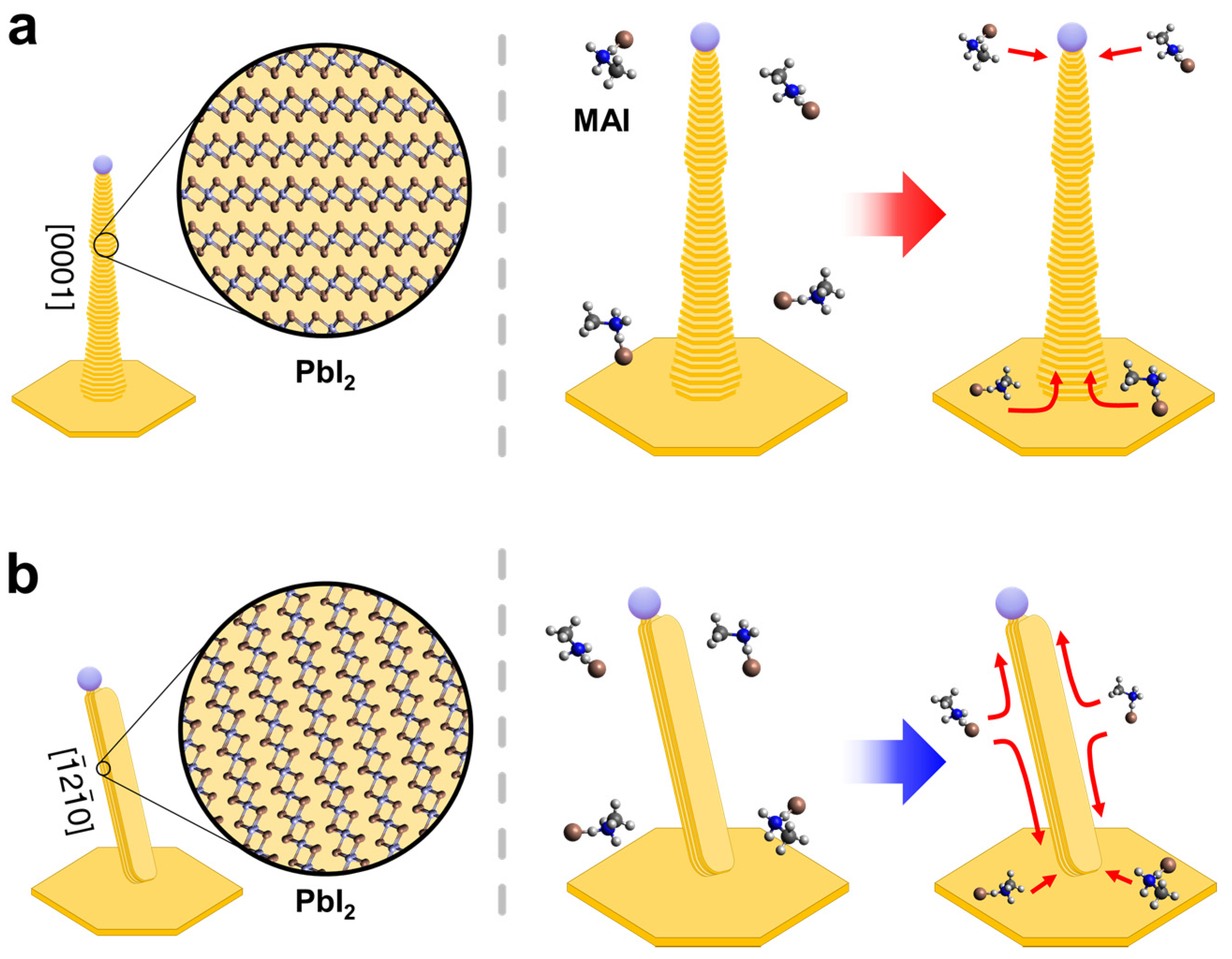
:1. Introduction
2. Materials and Methods
2.1. Sample Preparation and PbI2 Nanowire Growth
2.2. Conversion to MAPbI3
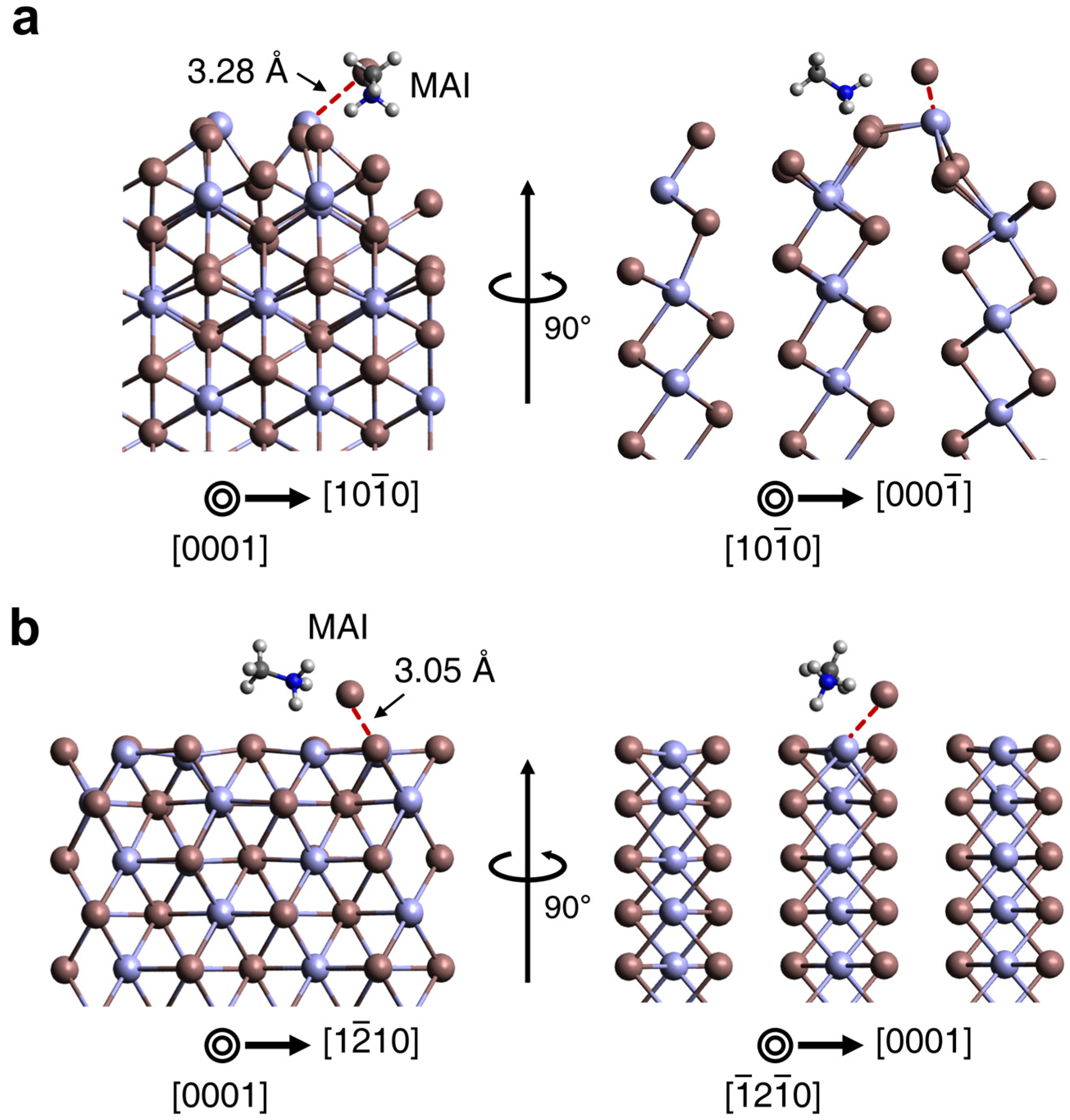
2.3. DFT Calculations
2.4. Characterization
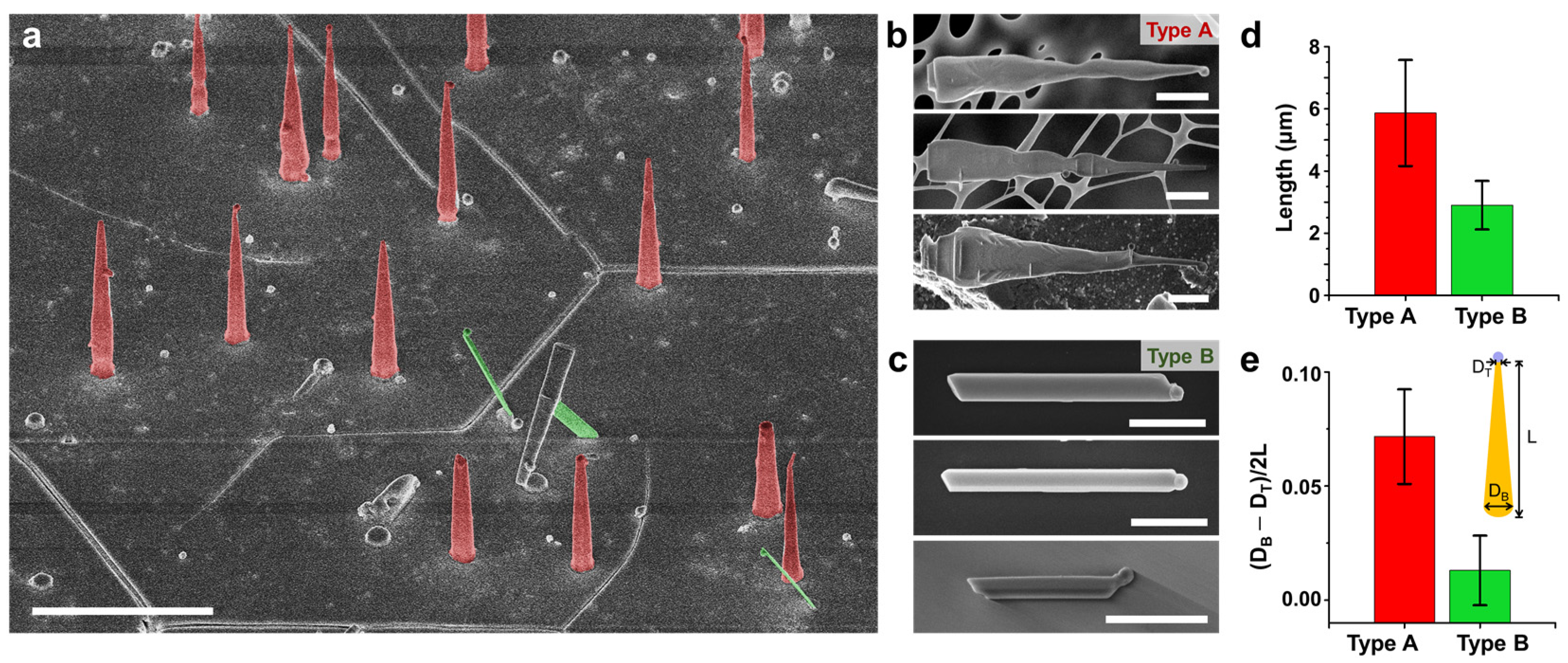
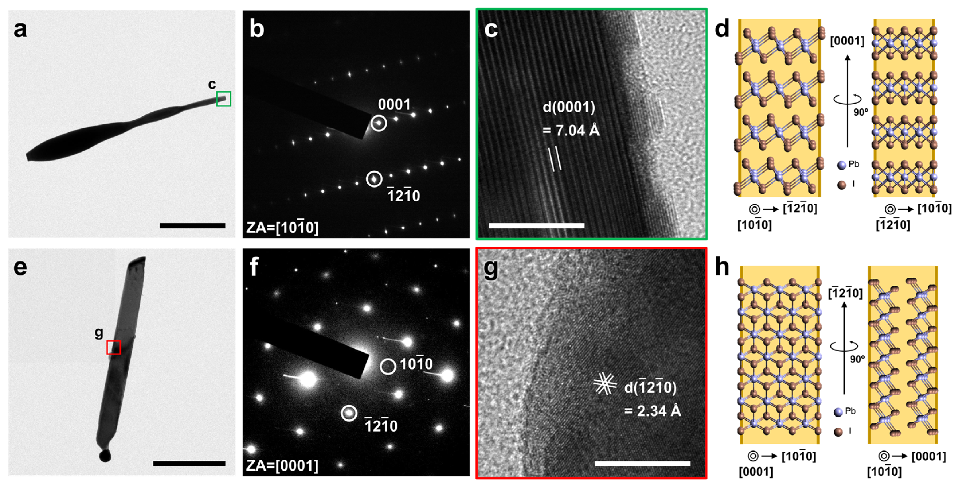
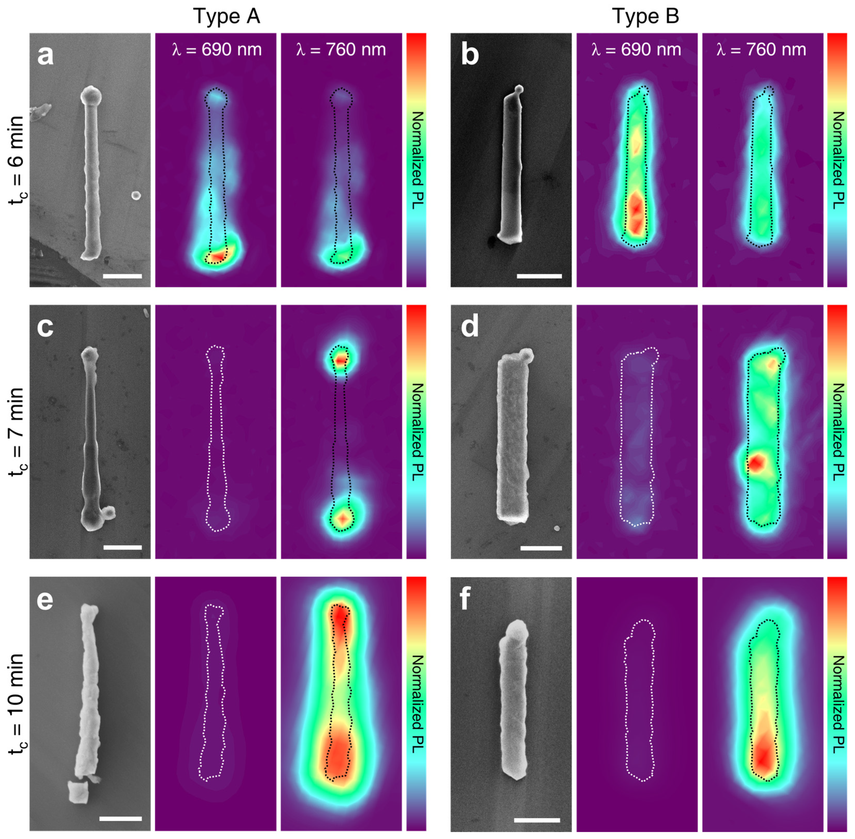
3. Results and Discussion
4. Conclusions
Supplementary Materials
Author Contributions
Funding
Data Availability Statement
Conflicts of Interest
References
- Xing, G.; Mathews, N.; Sun, S.; Lim, S.S.; Lam, Y.M.; Grätzel, M.; Mhaisalkar, S.; Sum, T.C. Long-Range Balanced Electron- and Hole-Transport Lengths in Organic-Inorganic CH3NH3PbI3. Science 2013, 342, 344–347. [Google Scholar] [CrossRef]
- Dong, Q.; Fang, Y.; Shao, Y.; Mulligan, P.; Qiu, J.; Cao, L.; Huang, J. Electron-Hole Diffusion Lengths > 175 μm in Solution-Grown CH3NH3PbI3 Single Crystals. Science 2015, 347, 967–970. [Google Scholar] [CrossRef] [PubMed] [Green Version]
- Wang, G.; Li, D.; Cheng, H.C.; Li, Y.; Chen, C.Y.; Yin, A.; Zhao, Z.; Lin, Z.; Wu, H.; He, Q.; et al. Wafer-Scale Growth of Large Arrays of Perovskite Microplate Crystal for Functional Electronics and Optoelectronics. Sci. Adv. 2015, 1, e1500613. [Google Scholar] [CrossRef] [PubMed] [Green Version]
- Lee, W.; Lee, J.; Yun, H.; Kim, J.; Park, J.; Choi, C.; Kim, D.C.; Seo, H.; Lee, H.; Yu, J.W.; et al. High-Resolution Spin-on-Patterning of Perovskite Thin Films for a Multiplexed Image Sensor Array. Adv. Mater. 2017, 29, 1702902. [Google Scholar] [CrossRef] [PubMed]
- Wu, W.; Wang, X.; Han, X.; Yang, Z.; Gao, G.; Zhang, Y.; Hu, J.; Tan, Y.; Pan, A.; Pan, C. Flexible Photodetector Arrays Based on Patterned CH3NH3PbI3−xClx Perovskite Film for Real-Time Photosensing and Imaging. Adv. Mater. 2019, 31, 1805913. [Google Scholar] [CrossRef]
- Zhang, N.; Fan, Y.; Wang, K.; Gu, Z.; Wang, Y.; Ge, L.; Xiao, S.; Song, Q. All-Optical Control of Lead Halide Perovskite Microlasers. Nat. Commun. 2019, 10, 1770. [Google Scholar] [CrossRef] [PubMed]
- Stylianakis, M.M.; Maksudov, T.; Panagiotopoulos, A.; Kakavelakis, G.; Petridis, K. Inorganic and Hybrid Perovskite Based Laser Devices: A Review. Materials 2019, 12, 859. [Google Scholar] [CrossRef] [PubMed] [Green Version]
- Schlaus, A.P.; Spencer, M.S.; Zhu, X. Light–Matter Interaction and Lasing in Lead Halide Perovskites. Acc. Chem. Res. 2019, 52, 2950. [Google Scholar] [CrossRef]
- Jana, S.; Carlos, E.; Panigrahi, S.; Martins, R.; Fortunato, E. Toward Stable Solution-Processed High-Mobility p-Type Thin Film Transistors Based on Halide Perovskites. ACS Nano 2020, 14, 14790–14797. [Google Scholar] [CrossRef]
- She, X.-J.; Chen, C.; Divitini, G.; Zhao, B.; Li, Y.; Wang, J.; Orri, J.F.; Cui, L.; Xu, W.; Peng, J.; et al. A solvent-based surface cleaning and passivation technique for suppressing ionic defects in high-mobility perovskite field-effect transistors. Nat. Electron. 2020, 3, 694–703. [Google Scholar] [CrossRef]
- Jaramillo-Quintero, O.A.; Sanchez, R.S.; Rincon, M.; Mora-Sero, I. Bright Visible-Infrared Light Emitting Diodes Based on Hybrid Halide Perovskite with Spiro-OMeTAD as a Hole-Injecting Layer. J. Phys. Chem. Lett. 2015, 6, 1883–1890. [Google Scholar] [CrossRef] [PubMed]
- Han, H.; Jeong, B.; Park, T.H.; Cha, W.; Cho, S.M.; Kim, Y.; Kim, H.H.; Kim, D.; Ryu, D.Y.; Choi, W.K.; et al. Highly Photoluminescent and Environmentally Stable Perovskite Nanocrystals Templated in Thin Self Assembled Block Copolymer Films. Adv. Funct. Mater. 2019, 29, 1808193. [Google Scholar] [CrossRef]
- Sapori, D.; Kepenekian, M.; Pedesseau, L.; Katan, C.; Even, J. Quantum Confinement and Dielectric Profiles of Colloidal Nanoplatelets of Halide Inorganic and Hybrid Organic−Inorganic Perovskites. Nanoscale 2016, 8, 6369–6378. [Google Scholar] [CrossRef] [PubMed] [Green Version]
- Zhang, D.; Gu, L.; Zhang, Q.; Lin, Y.; Lien, D.H.; Kam, M.; Poddar, S.; Garnett, E.C.; Javey, A.; Fan, Z. Increasing Photoluminescence Quantum Yield by Nanophotonic Design of Quantum-Confined Halide Perovskite Nanowire Arrays. Nano Lett. 2019, 19, 2850–2857. [Google Scholar] [CrossRef] [PubMed]
- Jiang, X.; Xiong, Q.; Nam, S.; Qian, F.; Li, Y.; Lieber, C.M. InAs/InP radial nanowire heterostructures as high electron mobility devices. Nano Lett. 2007, 7, 3214–3218. [Google Scholar] [CrossRef] [PubMed] [Green Version]
- Kempa, T.J.; Tian, B.; Kim, D.R.; Hu, J.; Zheng, X.; Lieber, C.M. Single and tandem axial pin nanowire photovoltaic devices. Nano Lett. 2008, 8, 3456–3460. [Google Scholar] [CrossRef]
- Um, H.D.; Moiz, S.A.; Park, K.T.; Jung, J.Y.; Jee, S.W.; Ahn, C.H.; Kim, D.C.; Cho, H.K.; Kim, D.W.; Lee, J.H. Highly selective spectral response with enhanced responsivity of n-ZnO/p-Si radial heterojunction nanowire photodiodes. Appl. Phys. Lett. 2011, 98, 033102. [Google Scholar] [CrossRef]
- Wagner, R.S.; Ellis, W.C. Vapor-Liquid-Solid Mechanism of Single Crystal Growth. Appl. Phys. Lett. 1964, 4, 89–90. [Google Scholar] [CrossRef]
- Morales, A.M.; Lieber, C.M. A Laser Ablation Method for the Synthesis of Crystalline Semiconductor Nanowires. Science 1998, 279, 208–211. [Google Scholar] [CrossRef]
- Shin, N.; Chi, M.; Filler, M.A. Interplay between Defect Propagation and Surface Hydrogen in Silicon Nanowire Kinking Superstructures. ACS Nano 2014, 8, 3829–3835. [Google Scholar] [CrossRef]
- Schmidt, V.; Wittemann, J.V.; Gösele, U. Growth, Thermodynamics, and Electrical Properties of Silicon Nanowires. Chem. Rev. 2010, 110, 361–388. [Google Scholar] [CrossRef] [PubMed] [Green Version]
- Barrigón, E.; Heurlin, M.; Bi, Z.; Monemar, B.; Samuelson, L. Synthesis and Applications of III-V Nanowires. Chem. Rev. 2019, 119, 9170–9220. [Google Scholar] [CrossRef] [PubMed]
- Madras, P.; Dailey, E.; Drucker, J. Kinetically Induced Kinking of Vapor−Liquid−Solid Grown Epitaxial Si Nanowires. Nano Lett. 2009, 9, 3826–3830. [Google Scholar] [CrossRef] [PubMed]
- Sun, Z.; Siedman, D.N.; Lauhon, L.J. Nanowire Kinking Modulates Doping Profiles by Reshaping the Liquid–Solid Growth Interface. Nano Lett. 2017, 17, 4518–4525. [Google Scholar] [CrossRef] [PubMed]
- Kim, S.; Hill, D.J.; Pinion, C.W.; Christesen, J.D.; McBride, J.R.; Cahoon, J.F. Designing Morphology in Epitaxial Silicon Nanowires: The Role of Gold, Surface Chemistry, and Phosphorus Doping. ACS Nano 2017, 11, 4453–4462. [Google Scholar] [CrossRef] [PubMed]
- Güniat, L.; Martí-Sánchez, S.; Garcia, O.; Boscardin, M.; Vindice, D.; Tappy, N.; Friedl, M.; Kim, W.; Zamani, M.; Francaviglia, L.; et al. III–V Integration on Si(100): Vertical Nanospades. ACS Nano 2019, 13, 5833–5840. [Google Scholar] [CrossRef] [Green Version]
- Johansson, J.; Dick, K.A. Recent advances in semiconductor nanowire heterostructures. CrystEngComm 2011, 13, 7175–7184. [Google Scholar] [CrossRef] [Green Version]
- Li, S.; Lin, Y.-C.; Zhao, W.; Wu, J.; Wang, Z.; Hu, Z.; Shen, Y.; Tang, D.-M.; Wang, J.; Zhang, Q.; et al. Vapor-Liquid-Solid Growth of Monolayer MoS2 Nanoribbons. Nat. Mater. 2018, 17, 535–542. [Google Scholar] [CrossRef] [Green Version]
- Huang, L.; Thi, Q.H.; Zheng, F.; Chen, X.; Chu, Y.W.; Lee, C.-S.; Zhao, J.; Ly, T.H. Catalyzed Kinetic Growth in Two-Dimensional MoS2. J. Am. Chem. Soc. 2020, 142, 13130–13135. [Google Scholar] [CrossRef]
- Sutter, P.; Wimer, S.; Sutter, E. Chiral twisted van der Waals nanowires. Nature 2019, 570, 354–357. [Google Scholar] [CrossRef]
- Sutter, E.; French, J.S.; Sutter, S.; Idrobo, J.C.; Sutter, P. Vapor–liquid–solid Growth and Optoelectronics of Gallium Sulfide van der Waals Nanowires. ACS Nano 2020, 14, 6117–6126. [Google Scholar] [CrossRef] [PubMed]
- Meyers, J.K.; Kim, S.; Hill, D.J.; Cating, E.E.; Williams, L.J.; Kumbhar, A.S.; McBride, J.R.; Papanikolas, J.M.; Cahoon, J.F. Self-Catalyzed Vapor−Liquid−Solid Growth of Lead Halide Nanowires and Conversion to Hybrid Perovskites. Nano Lett. 2017, 17, 7561–7568. [Google Scholar] [CrossRef] [PubMed]
- Shim, H.; Shin, N. VLS Homoepitaxy of Lead Iodide Nanowires for Hybrid Perovskite Conversion. J. Phys. Chem. Lett. 2019, 10, 6741–6749. [Google Scholar] [CrossRef] [PubMed]
- Grimme, S.; Antony, J.; Ehrlich, S.; Krieg, H. A consistent and accurate ab initio parametrization of density functional dispersion correction (DFT-D) for the 94 elements H-Pu. J. Chem. Phys. 2010, 132, 154104. [Google Scholar] [CrossRef] [PubMed] [Green Version]
- Grimme, S.; Ehrlich, S.; Goerigk, L. Effect of the damping function in dispersion corrected density functional theory. J. Comput. Chem. 2011, 32, 1456–1465. [Google Scholar] [CrossRef]
- Becke, A.D.; Johnson, E.R. A density-functional model of the dispersion interaction. J. Chem. Phys. 2005, 123, 154101. [Google Scholar] [CrossRef]
- Johnson, E.R.; Becke, A.D. A post-Hartree-Fock model of intermolecular interactions: Inclusion of higher-order corrections. J. Chem. Phys. 2006, 124, 174104. [Google Scholar] [CrossRef]
- Kresse, G.; Furthmüller, J. Efficient Iterative Schemes for Ab Initio Total-Energy Calculations Using a Plane-wave Basis Set. Phys. Rev. B 1996, 54, 11169–11186. [Google Scholar] [CrossRef]
- Kresse, G.; Furthmüller, J. Efficiency of Ab-initio Total Energy Calculations for Metals and Semiconductors Using a Plane-wave Basis Set. Comput. Mater. Sci. 1996, 6, 15–50. [Google Scholar] [CrossRef]
- Perdew, J.P.; Burke, K.; Ernzerhof, M. Generalized Gradient Approximation Made Simple. Phys. Rev. Lett. 1996, 77, 3865–3868. [Google Scholar] [CrossRef] [Green Version]
- Monkhorst, H.J.; Pack, J.D. Special Points for Brillouin-Zone Integrations. Phys. Rev. B 1976, 13, 5188–5192. [Google Scholar] [CrossRef]
- Bengtsson, L. Dipole Correction for Surface Supercell Calculations. Phys. Rev. B Condens. Matter Mater. Phys. 1999, 59, 12301–12304. [Google Scholar] [CrossRef]
- Neugebauer, J.; Scheffler, M. Adsorbate-Substrate and Adsorbate-Adsorbate Interactions of Na and K Adlayers on Al(111). Phys. Rev. B Condens. Matter Mater. Phys. 1992, 46, 16067–16080. [Google Scholar] [CrossRef] [PubMed] [Green Version]
- Sholl, D.S.; Steckel, J.A. Density Functional Theory: A Practical Introduction; John Wiley & Sons, Inc.: Hoboken, NJ, USA, 2009. [Google Scholar]
- Meng, Y.; Lan, C.; Li, F.; Yip, S.; Wei, R.; Kang, X.; Bu, X.; Dong, R.; Zhang, H.; Ho, J.C. Direct Vapor-Liquid-Solid Synthesis of All-Inorganic Perovskite Nanowires for High-Performance Electronics and Optoelectronics. ACS Nano 2019, 13, 6060–6070. [Google Scholar] [CrossRef] [PubMed]
- Meng, Y.; Lai, Z.; Li, F.; Wang, W.; Yip, S.; Quan, Q.; Bu, X.; Wang, F.; Bao, Y.; Hosomi, T.; et al. Perovskite Core–Shell Nanowire Transistors: Interfacial Transfer Doping and Surface Passivation. ACS Nano 2020, 14, 12749–12760. [Google Scholar] [CrossRef] [PubMed]
- Wang, Y.; Schmidt, V.; Senz, S.; Gösele, U. Epitaxial growth of silicon nanowires using an aluminum catalyst. Nat. Nanotechnol. 2006, 1, 186–189. [Google Scholar] [CrossRef]
- Zhong, M.; Zhang, S.; Huang, L.; You, J.; Wei, Z.; Liu, X.; Li, J. Large-Scale 2D PbI2 Monolayers: Experimental Realization and Their Indirect Band-Gap Related Properties. Nanoscale 2017, 9, 3736–3741. [Google Scholar] [CrossRef]
- Ross, F.M.; Tersoff, J.; Reuter, M.C. Sawtooth Faceting in Silicon Nanowires. Phys. Rev. Lett. 2005, 95, 146104. [Google Scholar] [CrossRef]


| Surface | |
|---|---|
| PbI2 () | −2.208 |
| PbI2 () | −1.525 |
Publisher’s Note: MDPI stays neutral with regard to jurisdictional claims in published maps and institutional affiliations. |
© 2021 by the authors. Licensee MDPI, Basel, Switzerland. This article is an open access article distributed under the terms and conditions of the Creative Commons Attribution (CC BY) license (http://creativecommons.org/licenses/by/4.0/).
Share and Cite
Shim, H.; Hwang, Y.; Kang, S.G.; Shin, N. Orientation-Dependent Conversion of VLS-Grown Lead Iodide Nanowires into Organic-Inorganic Hybrid Perovskites. Nanomaterials 2021, 11, 223. https://doi.org/10.3390/nano11010223
Shim H, Hwang Y, Kang SG, Shin N. Orientation-Dependent Conversion of VLS-Grown Lead Iodide Nanowires into Organic-Inorganic Hybrid Perovskites. Nanomaterials. 2021; 11(1):223. https://doi.org/10.3390/nano11010223
Chicago/Turabian StyleShim, Hyewon, Yunjeong Hwang, Sung Gu Kang, and Naechul Shin. 2021. "Orientation-Dependent Conversion of VLS-Grown Lead Iodide Nanowires into Organic-Inorganic Hybrid Perovskites" Nanomaterials 11, no. 1: 223. https://doi.org/10.3390/nano11010223