Article

Inversion Method Characterization of Graphene-Based Coordination Absorbers Incorporating Periodically Patterned Metal Ring Metasurfaces

1
School of Science, Jiangnan University, Wuxi 214122, China
2
Departments of Optics and General Physics, Francisk Skorina Gomel State University, Sovetskaya Str. 104, 246019 Gomel, Belarus
3
National Laboratory of Solid State Microstructures, Nanjing University, Nanjing 210093, China
*
Author to whom correspondence should be addressed.
Nanomaterials 2020, 10(6), 1102; https://doi.org/10.3390/nano10061102
Submission received: 9 May 2020 / Revised: 27 May 2020 / Accepted: 30 May 2020 / Published: 2 June 2020

Abstract

:
In this paper, we propose a tunable coordinated multi-band absorber that combines graphene with metal–dielectric–metal structures for the realization of multiple toward perfect absorption. The parametric inversion method is used to extract the equivalent impedance and explain the phenomena of multiple-peak absorption. With the change of the Fermi level, equivalent impedances were extracted, and the peculiarities of the individual multiple absorption peaks to change were determined. By changing the structure parameters of gold rings, we obtain either multiple narrow-band absorption peaks or a broadband absorption peak, with the bandwidth of 0.8 μm where the absorptance is near 100%. Therefore, our results provide new insights into the development of tunable multi-band absorbers and broadband absorbers that can be applied to terahertz imaging in high-performance coordinate sensors and other promising optoelectronic devices.

1. Introduction

Metamaterials are artificially structured materials that can have negative permittivity or/and permeability, which can be achieved by periodic metal–dielectric arrays [1,2,3,4]. With the advent of metamaterials, new feasibilities have been arisen for devices related to stealth technologies [5,6], hyperlenses [7], and high-sensitivity sensors [8]. Metamaterial-based absorbers (MMA) have gained wide attention since the first near-perfect metamaterial absorber was designed by N. I. Landy et al. [9]. MMAs are generally constructed by metal–dielectric–metal (MDM) multilayers. By adjusting the geometric or material parameters, the metamaterial can be tuned for different operating frequencies, which are crucial for actual manufacturing and different from sensors [10], filters [11], solar photovoltaic devices [12], etc. Nonetheless, the design of some devices based on metamaterials [13,14,15] have a common disadvantage: that is, the devices’ operating frequencies cannot be adjusted according to different requirements. This has become a major obstacle hindering the further development of MMAs toward tunable MMAs. To challenge this drawback, we here report that the implementation of a single layer of graphene [16] into properly designed MMA structures can achieve tunable operating frequencies.
Graphene is a relatively new two-dimensional sheet composed of carbon atoms of atomic thickness with unique quantum, thermodynamic [17], and optical properties [18,19]. Due to its special optical properties, relating, first of all, to the high transmittance of surface plasmons (SP) [20,21,22], light propagation controlling at sub-wavelength distances in the structure of metamaterials is providing a powerful tool in nanophotonics. Graphene surface plasmon resonance (SPR) is supported in a wide frequency range including infrared and terahertz bands [23,24,25,26] such that it is perfect for designing tunable active metamaterials. Moreover, being adaptable to the Fermi level tuned by applying an external voltage or chemical doping [27], graphene can optimize the operating frequencies of the whole graphene-based metamaterial devices at their fixed geometrical parameters [28,29,30,31,32]. Therefore, the combination of graphene with an MDM structure to design a dynamically adjustable perfect absorber seems is promising.
While the proposed novel, multi-band, and tunable selective absorber utilizes graphene as its key component, its base structure uses gold as a ground plane that reflects electromagnetic waves. Between the ground plane and graphene, a substrate layer of SiO2 is situated, while the top layer represents an array of different sized gold rings (see – 1). The proposed structure is simulated using the commercial finite element method (FEM) solver COMSOL Multiphysics with the purpose of obtaining a number of closely located near-perfect absorption peaks. For reliability purposes, an additional numerical simulation utilizing the method of inverse parameter extraction is carried out to extract effective parameters and explain the phenomenon of multiple absorption peaks. By adjusting the Fermi level of graphene, at least three absorption peaks can be tunable between 8 μm (37.5 THz) and 14 μm (21.4 THz) while the structural changes in parameters of metal rings lead to a single wide absorption peak with an absorptance higher than 80%. The position of the single peak is also Fermi-level adjustable.

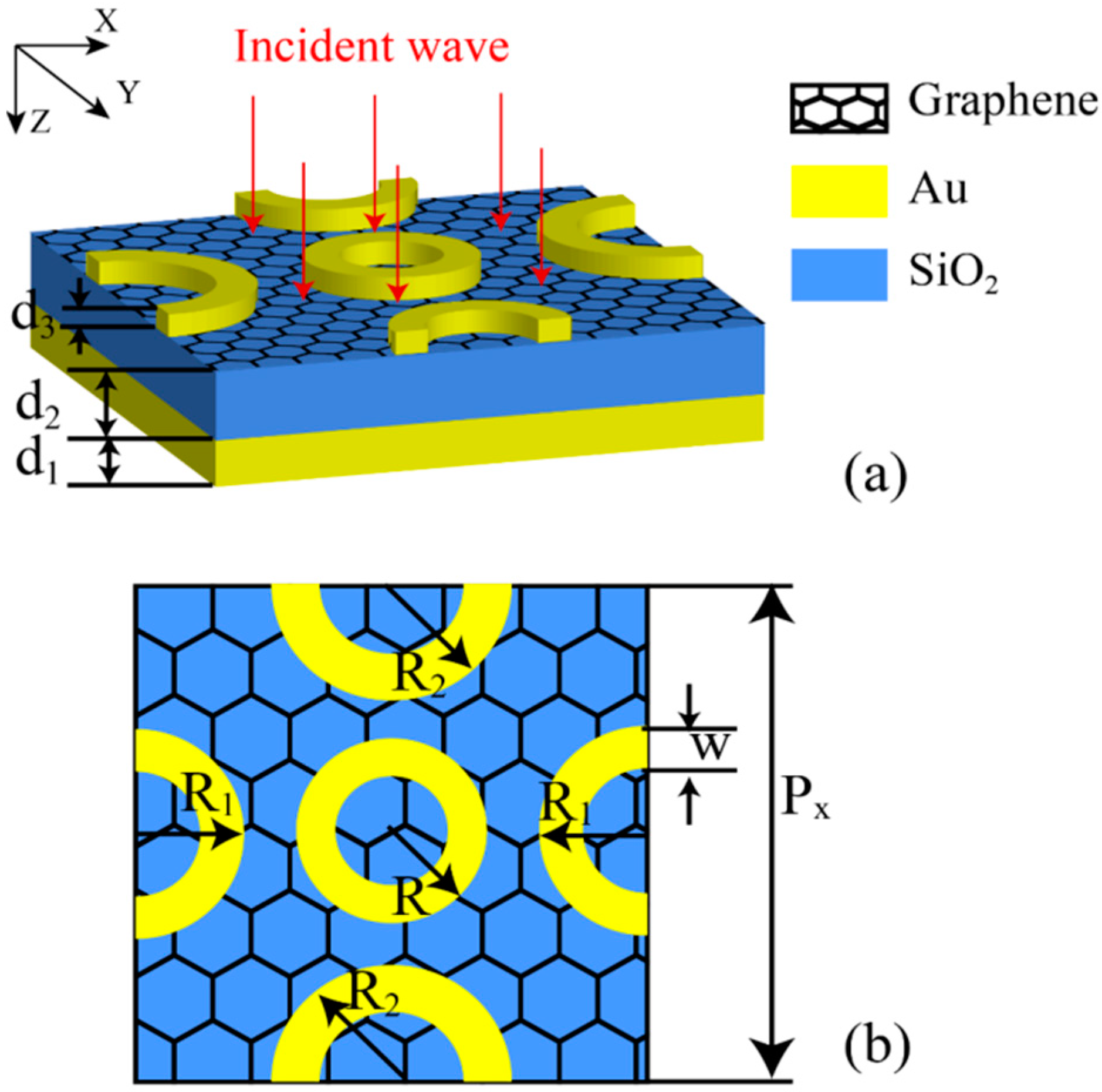
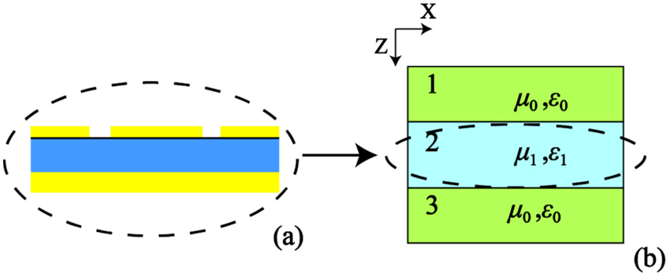
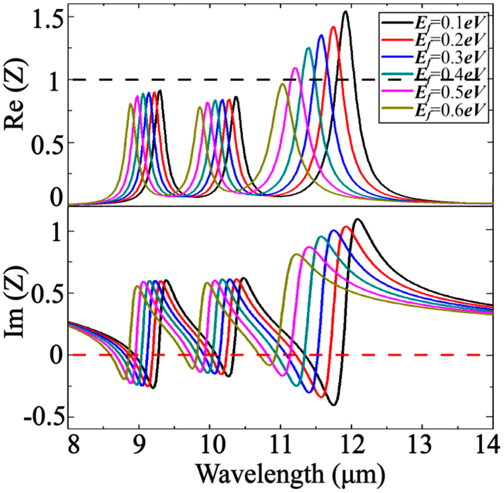
2. Design of the Absorber and Its Theoretical Analysis

The three-dimensional structure of the graphene-based selective absorber is proposed in Figure 1a indicating TM (Transverse Magnetic) waves in the incident XZ plane by red arrows. The yellow layer and rings represent gold with thicknesses of d1 and d3, respectively. The blue layer represents SiO2 with a thickness of d2. A single layer of graphene between the upper gold rings and the SiO2 substrate is pictured as a honeycomb structure. Within the operating wavelengths, the dispersion of dielectric constant of SiO2 [33] is negligible and therefore fixed at εSiO2 = 3.9, and the permittivity of gold can be expressed as ε = 1 − ( ω 2 p /(ω2 + iωγ)) using the Drude model [34] with the value of constant plasma frequency ωp = 1.36 × 10¹⁶ rad/s and collision frequency γ = 3.33 × 10¹³ rad/s. The graphene is simulated in COMSOL by setting the surface current density.
The Kubo formula describes the surface conductivity of graphene layers [35,36,37]:
σ g r a = σ int e r + σ int r a = 2 e 2 k B T π 2 i ω + i / τ ln [ 2 cosh ( E f 2 k B T ) ]     + e 2 4 2 [ 1 2 + 1 π arctan ( ω 2 E f 2 k B T ) i 2 π ln ( ω + 2 E f ) 2 ( ω 2 E f ) 2 + 4 ( k B T ) 2 ]
where σinter and σintra are expressed as the interband and intraband transition contributions, respectively. kB, ℏ, and e represent the Boltzmann constant, reduced Plank constant, and electron charge, respectively. ω is the angular frequency of the incident radiation, Ef is the graphene Fermi energy level, τ is the electron-phonon relaxation time, and T is the ambient temperature. As we only consider highly doped graphene, we should take into account that EfkBT and Ef ≫ ℏω. Therefore, the Kubo equation can be simplified to a Drude-like equation [38,39,40]:
σ gra = e 2 E f π 2 i ( ω + i / τ ) ,
where τ = μEf/( e v 2 F ), Ef is set to 0.15 eV, the media carrier mobility μ is set to 1318 cm2 V−1 s−1 [41], and the graphene Fermi velocity vF is set to 1 × 10⁶ ms−1. As shown in Figure 1a, the periodic boundary conditions for the unit cell are along the X and Y axes. Figure 1b is the top view of the unit cell. The outer ring radii of the three rings are R, R1, and R2 respectively, and the widths are all w. The optimal parameters of the absorber that can be considered as default parameters are the following: Px = 6.2 μm, d1 = 0.2 μm, d2 = 0.3 μm, d3 = 0.1 μm, R = 1.06 μm, R1 = 1.13 μm, R2 = 1.28 μm, and w = 0.44 μm.
The black curve in Figure 2a shows the absorptance spectrum for the absorber with default parameters. The obtained spectrum has three peaks of near-perfect absorption located at 9.24 μm, 10.3 μm, and 11.75 μm, respectively. It is important to investigate the influence of every individual group of rings R, R1, and R2 on the three absorptance peaks. Excluding all the rings from the structure except for (case A) – rings R, resulting in the green dotted line in Figure 2a with its peak at 9.54 μm; (case B) – rings R1, resulting in the red dotted line in Figure 2a with its peak at 10.21 μm; and (case C) – rings R2, resulting in the blue dotted line in Figure 2a with its peak at 11.61 μm. For the complex structure with a full set of rings in Figure 1, the absorptance is shown by the black curve in Figure 2a where all three separate peaks mentioned above take place. The purpose is to focus on the optimal parameters of the rings in a way that they can be excited individually (see Figure 2b–e) by the external radiation of three different frequencies, but at the same time, the sizes of rings are close to each other. Therefore, the peaks of absorptance are short-distanced and can be merged by applying specific external physical factors. Electric field distribution inside the rings in Figure 2b–e provides additional information facilitating precisely choosing the width of the rings, their outer coating, and the proper doping agent.
An inversion algorithm is applied to extract the normalized impedance of the multiple-peak absorber for explaining the physical mechanism of the phenomenon. The absorber is considered as a uniform layer with material parameters μ1 and ε1, which is surrounded by an outer layer with material parameters μ0 and ε0, as illustrated in Figure 3b. An incident wave, as before, propagates along the Z axis—that is, perpendicular to the surface of the absorber. For simplicity, layers 1 and 3 in Figure 3b represent air. The electromagnetic field strength in any conductive medium can be expressed as [42]:
E x = E x 0 e j k z E y = k μ ω E x 0 e j k z
When TM propagates in medium 1, without loss of generality, we set the amplitude Ex0 = 1. Then, the electromagnetic field strength in medium 1 can be written as:
E 1 x = e j k 1 z + Γ 1 e j k 1 z E 1 y = k 1 ω μ 0 e j k 1 x Γ 1 e j k 1 z
Then, the TM wave moves through the interface of medium 1 and medium 2, and the electromagnetic field strength in medium 2 can be written as:
E 2 x = τ 1 e j k 2 z + τ 1 Γ 2 e j k 2 z E 2 y = k 2 ω μ 1 ( τ 1 e j k 2 x τ 1 Γ 2 e j k 2 z )
Finally, the TM wave enters the medium 3, and the electromagnetic field strength in medium 3 can be written as:
E 3 x = τ 1 τ 2 e j k 3 z E 3 y = k 3 ω μ 0 τ 1 τ 2 e j k 3 z
where k1 = k3 = k0 is the wave number in vacuum, k2 = nk0 is the wave number in the relative medium, Γ1 and Γ2 are the reflection coefficients between medium 1 and medium 2, and medium 2 and medium 3, respectively. τ1 and τ2 are the transmission coefficients between medium 1 and medium 2, and medium 2 and medium 3, respectively.
We let the interface of medium 1 and medium 2 be the origin—that is, Z = 0. According to the boundary conditions encountered by the electromagnetic wave at the discontinuous interface when Z = 0, we can obtain:
{ E 1 x = E 2 x 1 + Γ 1 = τ 1 + τ 1 Γ 2 E 1 y = E 2 y k 1 ( 1 Γ 1 ) = k 2 μ r ( τ 1 τ 1 Γ 2 ) ,
and at Z = d, that is, at the interface between medium 2 and medium 3:
{ E 2 x = E 3 x τ 1 e j k 2 d + τ 1 Γ 2 e j k 2 d = τ 1 τ 2 e j k 3 d E 2 y = E 3 y k 2 μ r ( τ 1 e j k 2 d τ 1 Γ 2 e j k 2 d ) = k 3 τ 1 τ 2 e j k 3 d ,
According to the above-mentioned boundary conditions that the electromagnetic wave meets on the discontinuous interface, the scattering parameters can be obtained:
{ S 11 = Γ 1 ( 1 ( e j k 2 d ) 2 ) 1 ( Γ 1 e j k 2 d ) 2 S 21 = 1 Γ 1 2 1 ( Γ 1 e j k 2 d ) 2 e j k 2 d ,
where Γ1 = (Z − 1)/(Z + 1). Since we use gold as the reflective layer of the entire absorber, there is no transmission spectrum, so S21 = 0. According to the selection of the sign [43,44], we can get:
Z = ± ( 1 + S 11 ) 2 S 21 2 ( 1 S 11 ) 2 S 21 2 = 1 + S 11 1 S 11 ,
In order to minimize reflection, the normalized impedance of the absorber should be close enough to the impedance of free space—that is, the closer the real part of the normalized impedance is to unity and the closer the imaginary part is to vanishing, giving rise to the greater the absorptance of the structure. As is shown in Figure 4, three vertical dotted lines represent three resonance wavelength positions, and the positions of the first and second vertical dotted lines correspond to the first and second peaks of the real part of the impedance, respectively. The normalized impedances obtained at resonance wavelengths of 9.24 μm, 10.3 μm, and 11.75 μm are 0.9052 + 0.0378j, 0.8524 + 0.0760j, and 1.2099 − 0.1022j, respectively. The information is useful during optimizing the internal structure of the absorber as well as its composition with the purpose of minimizing the transmittance.
The relationship between the normalized impedance and the energy of Fermi level is investigated in Figure 5 to predict the absorptance properties when the graphed doping level is changing. As the Fermi level increases, the real and imaginary parts of the normalized impedance decrease slightly, and the resonance wavelength appears blue shifted. From this, we can see that as the Fermi level increases, the resonance wavelength of the absorber should appear blue shifted.

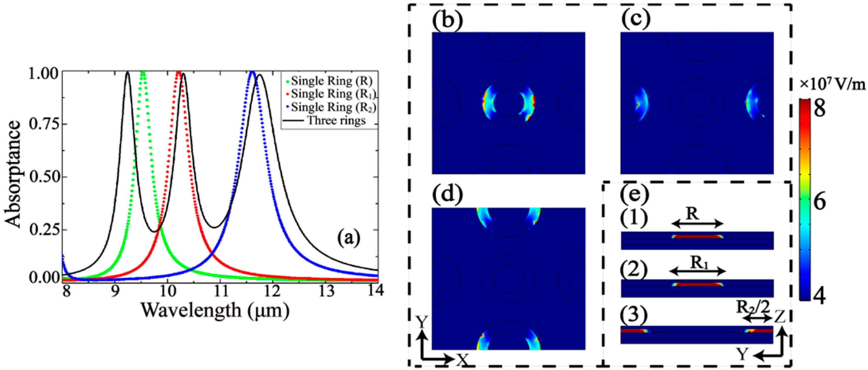
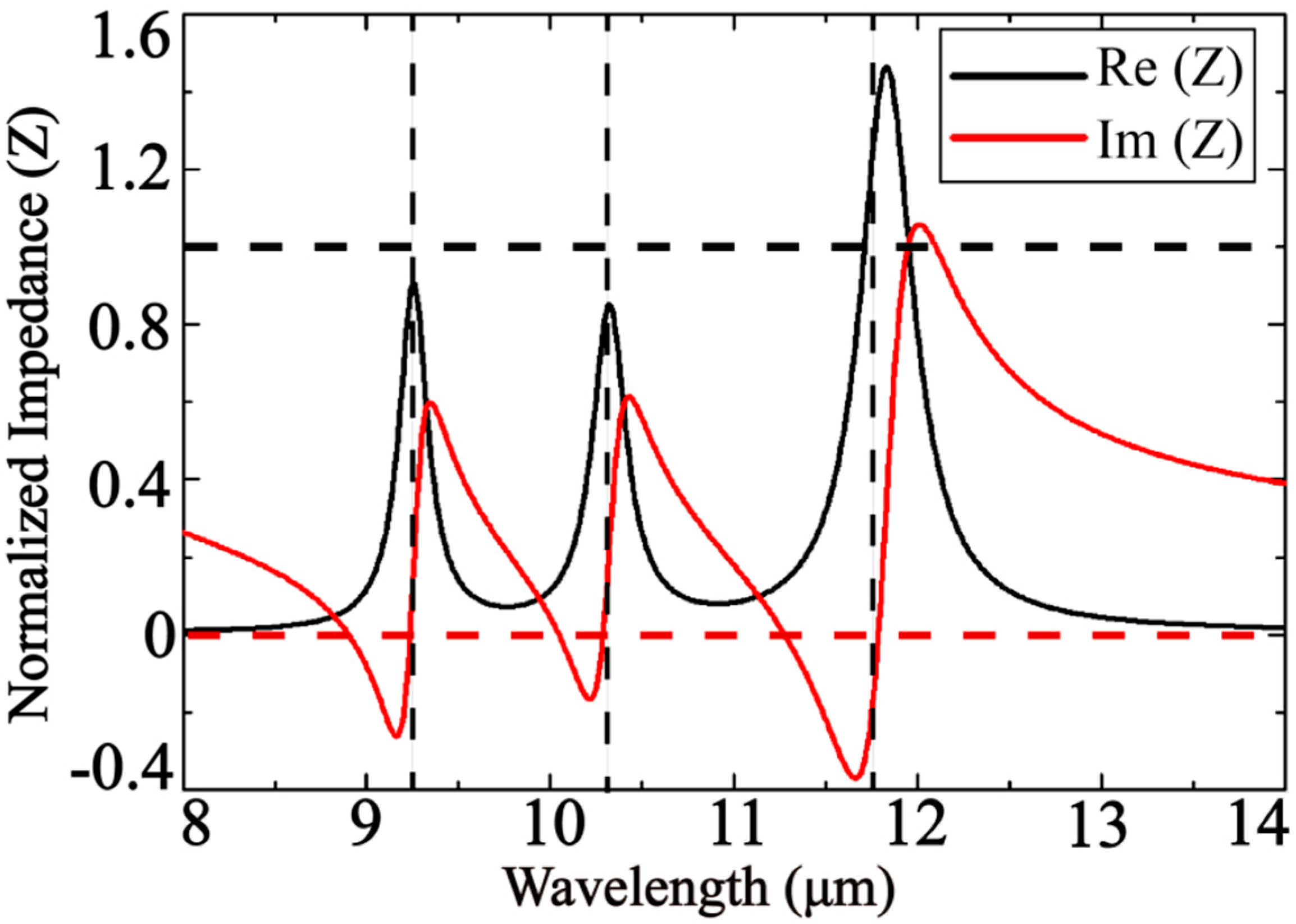
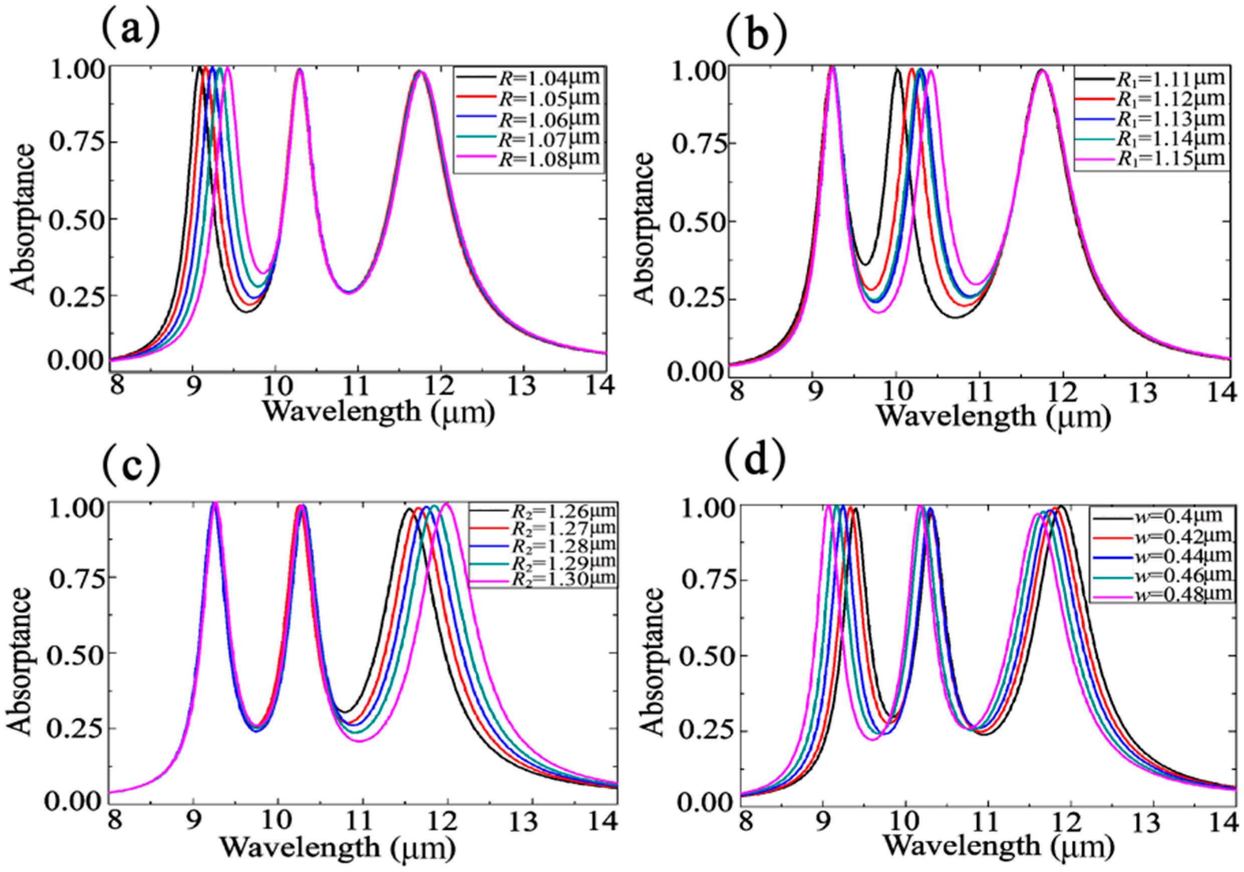
3. Absorptance Variational Analysis

In order to explore the dependence of peak displacement on structural parameters, we carry out a variation analysis. With R increasing independently from 1.04 μm to 1.08 μm, R1 increasing independently from 1.11 μm to 1.15 μm, and R2 increasing independently from 1.27 μm to 1.30 μm, the resonance wavelengths of the corresponding absorption peaks are red-shifted by 1.2 μm, 0.4 μm, and 0.4 μm respectively (see Figure 6a–c). The peak height is decreased by 0.4% during the first and second variation and by 1.6% for the third one. With increasing the width of the rings, all three resonance absorption peaks are blue shifted (see Figure 6d), while the peak height is increased slightly for the first and second, and it is decreased slightly for the third absorption peak. Thus, independent peak localization control is achievable by ring size adjustment.
The analysis of the change in the carrier mobility u in Figure 7 shows that when u increases, the first two absorptance peaks increase slightly, and the third absorption peak decreases significantly. This behavior is different from some previous patterned graphene multi-band absorbers [31,45]. We speculate that there is an interaction between the resonance absorption of the three metal rings and the single-layer graphene, thus forming such a changing behavior.
Since the structure proposed by us lays a layer of graphene, we can adjust the Fermi level of graphene by applying a voltage across the graphene, thereby changing the resonance frequency of the absorption peak. The Fermi level energy Ef variation analysis in Figure 8 shows that with increasing Ef from 0.1 to 0.6, all three absorption peaks are blue shifted by 0.4 μm, 0.5 μm, and 0.88 μm, respectively, while the peak heights are reduced slightly for the first two peaks and are increased slightly for the third one. The enhancement of the third peak is explained by the substantial reduction of the real part of the normalized impedance when increasing Ef (see Figure 5). Known from reference [46], the graphene plasma dispersion relation is:
k s p p = ω r 2 / ( 2 α 0 E f c ) = 2 π 2 c α 0 E f λ r 2 ,
where α0 = e2/(ℏc) is the structural constant of graphene, and λr is the polarization resonance wavelength of graphene. From the above formula, the resonance frequency of the plasmon surface of the graphene can be obtained: fr ∝ (α0Ef/(2π2ℏcL))1/2. That is, as the Fermi level increases, the resonant frequency also increases.

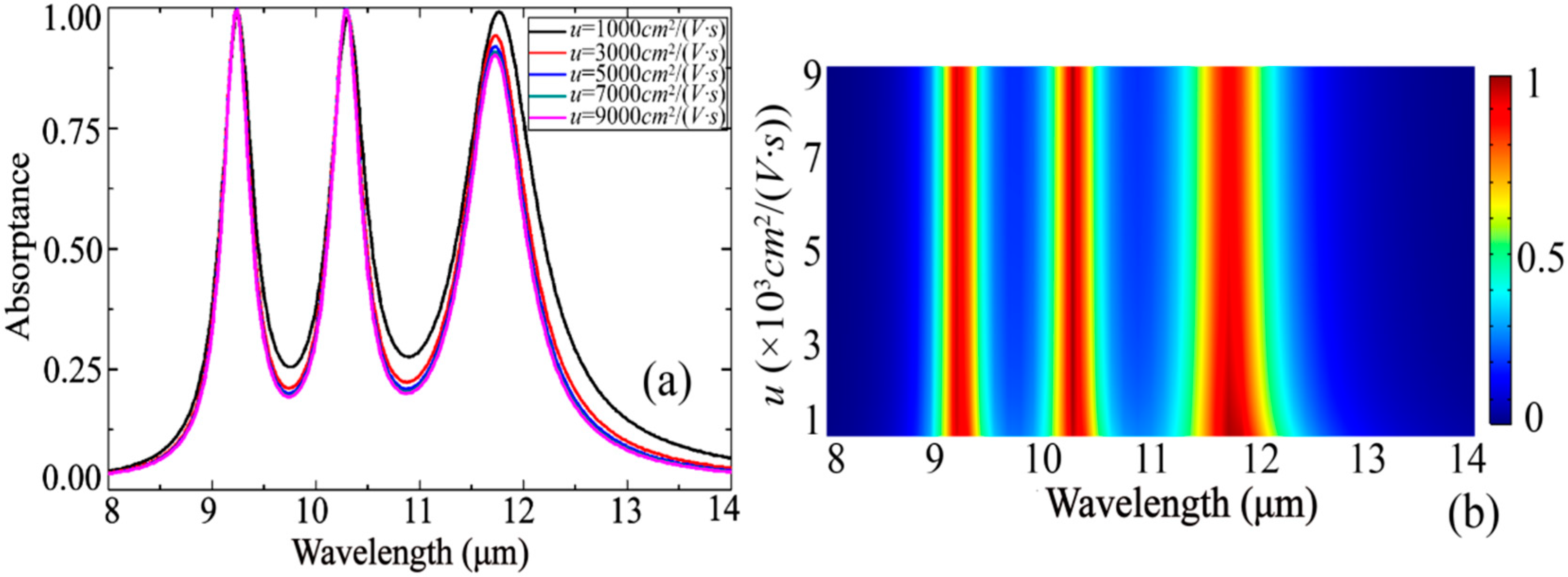
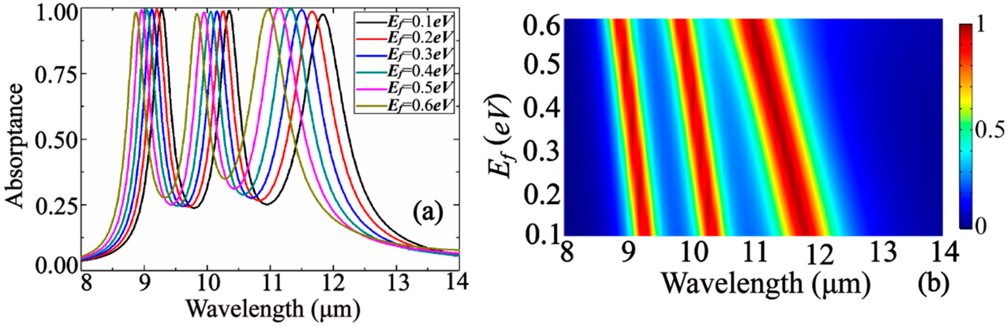
4. Dynamically Adjustable Narrowband/Broadband Absorber

For the technical applications that require one broad absorption band instead of three narrow peaks, a modified version of the ring-type absorber is proposed with structural parameters R = 1.06 μm, R1 = 1.24 μm, R2 = 1.26 μm, and w = 0.44 μm. In this case, the absorptance greater than 80% occurs between wavelengths 10.51 and 11.31 μm (see Figure 9a)—that is, the full width at half maximum for the absorption spectrum can reach up to 1.17 μm. The positioning of the peaks can be controlled within 0.76 μm by Fermi level energy Ef varying between 0.4 and 0.9 eV, as shown in Figure 9b.

5. Conclusions

We proposed a novel, multi-band, tunable selective absorber with ground plane, a graphene layer, and a complex combination of gold rings patterned on the graphene layers. Through continuous optimization of the structural parameters of the three metal rings, three perfect closely located absorptance peaks between 8 and 12 μm are achieved. A method for extracting the inversion parameters of the absorber is used for obtaining the effective impedance of the structure and explaining the appearance of the three absorption peaks. An influence of Fermi levels onto the absorptance peaks resonance frequency is also investigated. The simultaneous realization of a single narrowband and broadband (with 0.8 μm bandwidth) absorption peaks with an absorptance greater than 80% is achieved. We assume that our findings can potentially be useful in those practical applications relating to adjustable optical filters, splitters, modulators.

Author Contributions

Conceptualization, Z.B. and J.W.; methodology, C.Z.; software, Z.B.; validation, Y.T.; formal analysis, Z.-D.H.; investigation, Z.B.; resources, Z.B.; data curation, Z.B. and Y.T.; writing—original draft preparation, Z.B. and J.W.; writing—review and editing, A.B., S.K., and I.S.; visualization, Z.B.; supervision, J.W.; project administration, J.W.; funding acquisition, J.W. All authors have read and agreed to the published version of the manuscript.

Funding

This work was supported in part by the National Natural Science Foundation of China (Grant Nos. 11504139, 11504140, 11947028 11811530052), the Intergovernmental Science and Technology Regular Meeting Exchange Project of Ministry of Science and Technology of China (Grant No. CB02-20), the China Postdoctoral Science Foundation (Grant Nos. 2017M611693, 2018T110440), the Project of State Key Laboratory of Solid Microstructure Physics of Nanjing University (M32056), the State Committee for Science and Technology of Belarus (Grant No. F19KITG-017), the Graduate Research and Innovation Projects of Jiangsu Province (Grant No. JNKY19_052), the Training Programs of Innovation and Entrepreneurship for Undergraduates of Jiangsu Province and China (Grant Nos. 201910295051Z, 201910295067).

Conflicts of Interest

The authors declare no conflict of interest.

References

  1. Shalaev, V.M. Optical negative-index metamaterials. Nat. Photonics 2007, 1, 41–48. [Google Scholar] [CrossRef]
  2. Zheludev, N.I.; Kivshar, K.S. From metamaterials to metadevices. Nat. Mater. 2012, 11, 917–924. [Google Scholar] [CrossRef]
  3. Xing, X.; Li, Y.; Lu, Y.C.; Zhang, W.T.; Zhang, X.X.; Han, J.G.; Zhang, W.L. Terahertz metamaterial beam splitters based on untraditional coding scheme. Opt. Express 2019, 27, A1627–A1635. [Google Scholar] [CrossRef]
  4. Liu, S.; Chen, H.B.; Cui, T.J. A broadband terahertz absorber using multi-layer stacked bars. Appl. Phys. Lett. 2015, 106, 151601. [Google Scholar] [CrossRef]
  5. Schurig, D.; Mock, J.J.; Justice, B.J.; Cummer, S.A.; Pendry, J.B.; Starr, A.F.; Smith, D.R. Metamaterial electromagnetic cloak at microwave frequencies. Science 2006, 314, 977–980. [Google Scholar] [CrossRef] [Green Version]
  6. Vanbésien, O.; Fabre, N.; Mélique, X.; Lippens, D. Photonic-crystal–based cloaking device at optical wavelength. Appl. Opt. 2008, 47, 1358–1362. [Google Scholar] [CrossRef]
  7. Pendry, J.B. Negative refraction makes a perfect lens. Phys. Rev. Lett. 2000, 85, 3966–3969. [Google Scholar] [CrossRef]
  8. Liu, N.; Mesch, M.; Weiss, T.; Hentschel, M.; Giessen, H. Infrared perfect absorber and its application as plasmonic sensor. Nano Lett. 2010, 10, 2342–2348. [Google Scholar] [CrossRef]
  9. Landy, N.I.; Sajuyigbe, S.; Mock, J.J.; Smith, D.R.; Padilla, W.J. Perfect metamaterial absorber. Phys. Rev. Lett. 2008, 100, 207402. [Google Scholar] [CrossRef]
  10. Caucheteur, C.; Guo, T.; Liu, F.; Guan, B.O.; Albert, J. Ultrasensitive plasmonic sensing in air using optical fibre spectral combs. Nat. Commun. 2016, 7, 13371. [Google Scholar] [CrossRef] [Green Version]
  11. McCrindle, I.J.H.; Grant, J.; Drysdale, T.D.; Cumming, D.R.S. Multi-spectral materials: Hybridisation of optical plasmonic filters and a terahertz metamaterial absorber. Adv. Opt. Mater. 2014, 2, 149–153. [Google Scholar] [CrossRef] [Green Version]
  12. Liang, Q.Q.; Yu, W.X.; Zhao, W.C.; Wang, T.S.; Zhao, J.L.; Zhang, H.S.; Tao, S. Numerical study of the meta-nanopyramid array as efficient solar energy absorber. Opt. Mater. Express 2013, 3, 1187–1196. [Google Scholar] [CrossRef]
  13. Shchegolkov, D.Y.; Azad, A.K.; O’hara, J.F.; Simakov, E.I. Perfect subwavelength fishnetlike metamaterial-based film terahertz absorbers. Phys. Rev. B 2010, 82, 205117. [Google Scholar] [CrossRef]
  14. Alici, K.B.; Bilotti, F.; Vegni, L.; Ozbay, E. Experimental verification of metamaterial based subwavelength microwave absorbers. J. Appl. Phys. 2010, 108, 083113. [Google Scholar] [CrossRef]
  15. Wang, B.X.; Tang, C.; Niu, Q.; He, Y.; Chen, T. Design of Narrow Discrete Distances of Dual-/Triple-Band Terahertz Metamaterial Absorbers. Nanoscale Res. Lett. 2019, 14, 64. [Google Scholar] [CrossRef] [Green Version]
  16. Novoselov, K.S.; Geim, A.K.; Morozov, S.V.; Jiang, D.; Zhang, Y.; Dubonos, S.V.; Grigorieva, I.V.; Firsov, A.A. Electric field effect in atomically thin carbon films. Science 2004, 306, 666–669. [Google Scholar] [CrossRef] [Green Version]
  17. Mingo, N.; Broido, D.A. Carbon nanotube ballistic thermal conductance and its limits. Phys. Rev. Lett. 2005, 95, 096105. [Google Scholar] [CrossRef]
  18. Zhang, Y.B.; Tang, T.T.; Girit, C.; Hao, Z.; Martin, M.C.; Zettl, A.; Crommie, M.F.; Shen, Y.R.; Wang, F. Direct observation of a widely tunable bandgap in bilayer graphene. Nature 2009, 459, 820–823. [Google Scholar] [CrossRef]
  19. Han, Y.; Liu, Y.X.; Han, L.; Lin, J.; Jin, P. High-performance hierarchical graphene/metal-mesh film for optically transparent electromagnetic interference shielding. Carbon 2017, 115, 34–42. [Google Scholar] [CrossRef]
  20. He, X. Tunable terahertz graphene metamaterials. Carbon 2015, 82, 229–237. [Google Scholar] [CrossRef]
  21. Li, H.; Ji, C.; Ren, Y.; Hu, J.; Qin, M.; Wang, L. Investigation of multiband plasmonic metamaterial perfect absorbers based on graphene ribbons by the phase-coupled method. Carbon 2019, 141, 481–487. [Google Scholar] [CrossRef]
  22. Xia, S.X.; Zhai, X.; Wang, L.L.; Wen, S.C. Plasmonically induced transparency in double-layered graphene nanoribbons. Photonics Res. 2018, 6, 692–702. [Google Scholar] [CrossRef]
  23. Amin, M.; Farhat, M.; Bağcı, H. An ultra-broadband multilayered graphene absorber. Opt. Express 2013, 21, 29938–29948. [Google Scholar] [CrossRef] [PubMed]
  24. Ye, L.F.; Chen, Y.; Cai, G.X.; Liu, N.; Zhu, J.F.; Song, Z.Y.; Liu, Q.H. Broadband absorber with periodically sinusoidally-patterned graphene layer in terahertz range. Opt. Express 2017, 25, 11223–11232. [Google Scholar] [CrossRef]
  25. Yao, G.; Ling, F.R.; Yue, J.; Luo, C.Y.; Ji, J.; Yao, J.Q. Dual-band tunable perfect metamaterial absorber in the THz range. Opt. Express 2016, 24, 1518–1527. [Google Scholar] [CrossRef]
  26. Lu, H.; Gan, X.T.; Jia, B.H.; Mao, D.; Zhao, J.L. Tunable high-efficiency light absorption of monolayer graphene via Tamm plasmon polaritons. Opt. Lett. 2016, 41, 4743. [Google Scholar] [CrossRef]
  27. Ju, L.; Geng, B.S.; Horng, J.; Girit, C.; Martin, M.; Hao, Z.; Bechtel, H.A.; Liang, X.; Zettl, A.; Shen, Y.R.; et al. Graphene plasmonics for tunable terahertz metamaterials. Nat. Nanotechnol. 2011, 6, 630–634. [Google Scholar] [CrossRef]
  28. Woo, J.M.; Kim, M.S.; Kim, H.W.; Jang, J.H. Graphene based salisbury screen for terahertz absorber. Appl. Phys. Lett. 2014, 104, 081106. [Google Scholar]
  29. He, S.; Chen, T. Broadband THz absorbers with graphene-based anisotropic metamaterial films. IEEE Trans. Terahertz Sci. Technol. 2013, 3, 757–763. [Google Scholar] [CrossRef]
  30. Wang, J.; Yang, L.; Wang, M.; Hu, Z.D.; Deng, Q.; Nie, Y.; Zhang, F.; Sang, T. Perfect absorption and strong magnetic polaritons coupling of graphene-based silicon carbide grating cavity structures. J. Phys. D 2019, 52, 015101. [Google Scholar] [CrossRef]
  31. Xu, B.Z.; Gu, C.Q.; Li, Z.; Niu, Z.Y. A novel structure for tunable terahertz absorber based on graphene. Opt. Express 2013, 21, 23803–23811. [Google Scholar] [CrossRef]
  32. Bao, Z.Y.; Wang, J.C.; Hu, Z.D.; Balmakou, A.; Khakhomov, S.; Zhang, C.J. Coordinated multi-band angle insensitive selection absorber based on graphene metamaterials. Opt. Express 2019, 27, 31435–31445. [Google Scholar] [CrossRef] [PubMed]
  33. Deng, X.H.; Liu, J.T.; Yuan, J.; Wang, T.B.; Liu, N.H. Tunable THz absorption in graphene-based heterostructures. Opt. Express 2014, 22, 30177–30183. [Google Scholar] [CrossRef]
  34. Jadidi, M.M.; Sushkov, A.B.; Myers-Ward, R.L.; Boyd, A.K.; Daniels, K.M.; Gaskill, D.K.; Fuhrer, M.S.; Drew, H.D.; Murphy, T.E. Tunable terahertz hybrid metal-graphene plasmons. Nano Lett. 2015, 15, 7099–7104. [Google Scholar] [CrossRef] [Green Version]
  35. Hwang, E.H.; Das Sarma, S. Dielectric function, screening, and plasmons in two-dimensional grapheme. Phys. Rev. B 2007, 75, 205418. [Google Scholar] [CrossRef] [Green Version]
  36. Falkovsky, L.A.; Pershoguba, S.S. Optical far-infrared properties of a graphene monolayer and multilayer. Phys. Rev. B 2007, 76, 153410. [Google Scholar] [CrossRef] [Green Version]
  37. Hanson, G.W. Dyadic Green’s functions and guided surface waves for a surface conductivity model of grapheme. J. Appl. Phys. 2008, 103, 064302. [Google Scholar] [CrossRef] [Green Version]
  38. Xiao, S.; Wang, T.; Liu, Y.; Xu, C.; Han, X.; Yan, X. Tunable light trapping and absorption enhancement with graphene ring arrays. Phys. Chem. Chem. Phys. 2016, 18, 26661–26669. [Google Scholar] [CrossRef] [Green Version]
  39. Ke, S.; Wang, B.; Huang, H.; Long, H.; Wang, K.; Lu, P. Plasmonic absorption enhancement in periodic crossshaped graphene arrays. Opt. Express 2015, 23, 8888–8900. [Google Scholar] [CrossRef]
  40. Jin, S.; Wang, X.; Han, P.; Sun, W.; Feng, S.; Zhang, Y.; Ye, J.S.; Zhang, C. Modulation of terahertz radiation from graphene surface plasmon polaritons via surface acoustic wave. Opt. Express 2019, 27, 11137–11151. [Google Scholar] [CrossRef]
  41. Liu, Y.; Zhong, R.B.; Huang, J.B.; Lv, Y.L.; Han, C.; Liu, S.G. Independently tunable multi-band and ultra-wide-band absorbers based on multilayer metal-graphene metamaterials. Opt. Express 2019, 27, 7393–7404. [Google Scholar] [CrossRef] [PubMed]
  42. Iskander, M.F. Electromagnetic Fields and Waves, 2nd ed.; Waveland Press: Long Grove, IL, USA, 2013. [Google Scholar]
  43. Smith, D.R.; Schultz, S.; Markoš, P.; Soukoulis, C.M. Determination of effective permittivity and permeability of metamaterials from reflection and transmission coefficients. Phys. Rev. B 2002, 65, 195104. [Google Scholar] [CrossRef] [Green Version]
  44. Smith, D.R.; Vier, D.C.; Koschny, T.; Soukoulis, C.M. Electromagnetic parameter retrieval from inhomogeneous metamaterials. Phys. Rev. E 2005, 71, 036617. [Google Scholar] [CrossRef] [PubMed] [Green Version]
  45. Wang, X.; Chen, C.; Pan, L.; Wang, J. A graphene-based Fabry-Pérot spectrometer in mid-infrared region. Sci. Rep. 2016, 6, 32616. [Google Scholar] [CrossRef] [PubMed] [Green Version]
  46. Koppens, F.H.; Chang, D.E. Graphene plasmonics: A platform for strong light-matter interactions. Nano Lett. 2011, 11, 3370–3377. [Google Scholar] [CrossRef] [PubMed] [Green Version]
Figure 1. (a) The elementary unit cell of the proposed structure; (b) the top view of the unit cell. The width of the outer ring of the three metal rings is R, R1, and R2, and the width of the three rings is w. The thickness of the three rings is d3.
Nanomaterials 10 01102 g001
Figure 2. (a) Absorptance spectra for the absorber in Figure 1 with complete or partial ring structure; (be) represent the top and side views of the electric field distribution inside the absorber structure at wavelength of excitation 9.24 μm, 10.3 μm, and 11.75 μm, respectively.
Nanomaterials 10 01102 g002
Figure 3. (a) Lateral schematic view of the absorber; (b) Equivalent model of the absorber.
Nanomaterials 10 01102 g003
Figure 4. Normalized impedance obtained by inversion algorithm.
Nanomaterials 10 01102 g004
Figure 5. Normalized impedance as a function of Fermi level.
Nanomaterials 10 01102 g005
Figure 6. (ad) Absorption spectra analysis with varying R, R1, R2, and w, respectively. Other parameters are set as default.
Nanomaterials 10 01102 g006
Figure 7. Carrier mobility variation analysis, (a) one-dimensional line diagram; (b) two-dimensional color diagram.
Nanomaterials 10 01102 g007
Figure 8. Fermi level energy variation analysis, (a) one-dimensional line diagram; (b) two-dimensional color diagram.
Nanomaterials 10 01102 g008
Figure 9. (a) The absorption spectrum for a modified absorber with the second and third peaks merged; (b) Fermi energy level variation analysis.
Nanomaterials 10 01102 g009

