An Implementation of Parallel Buck Converters for Common Load Sharing in DC Microgrid


Abstract
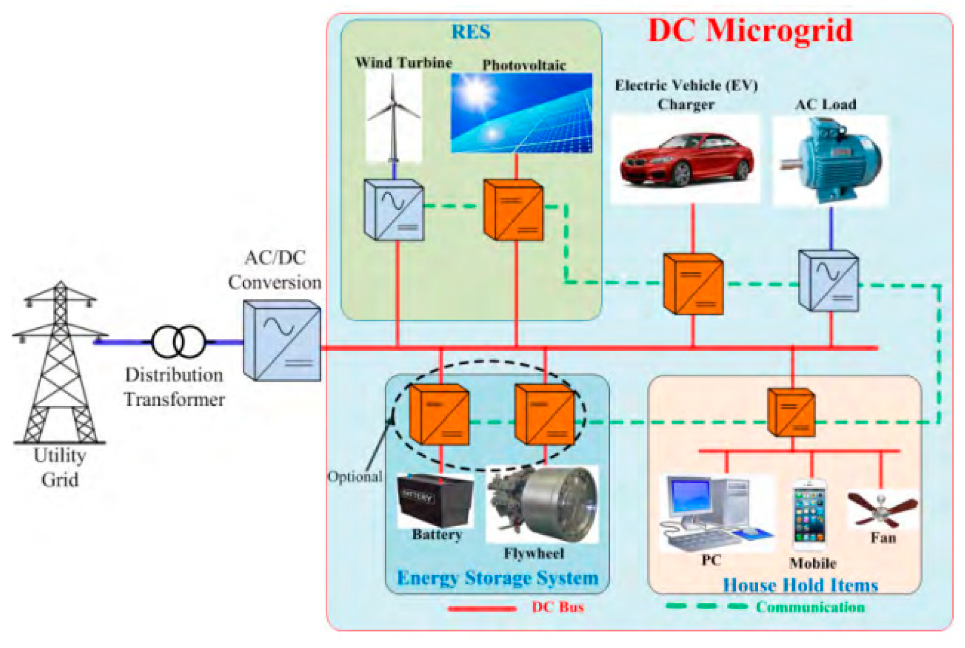
:1. Introduction
2. Modeling and Paralleling of the Buck Converters
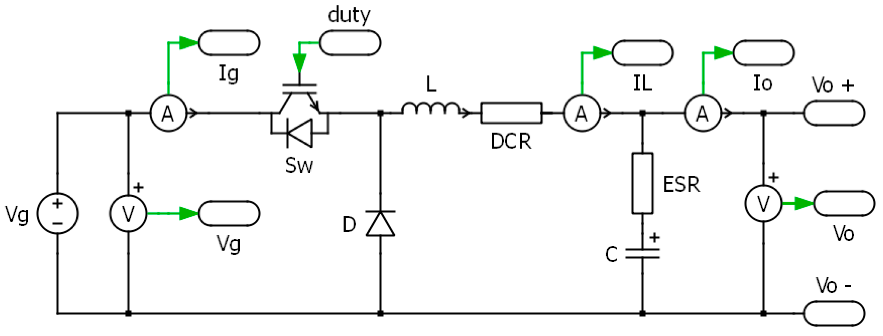
2.1. Buck Converters
- Vg = the source voltage
- Vo = the output voltage
- Sw = the switch (IGBT)
- Ig = Input Current
- IL = Inductor’s current
- IO = Output current
- D = the diode
- L = inductor
- C = Capacitor
- DCR = Inductor’s resistance
- ESR = Equivalent series resistance
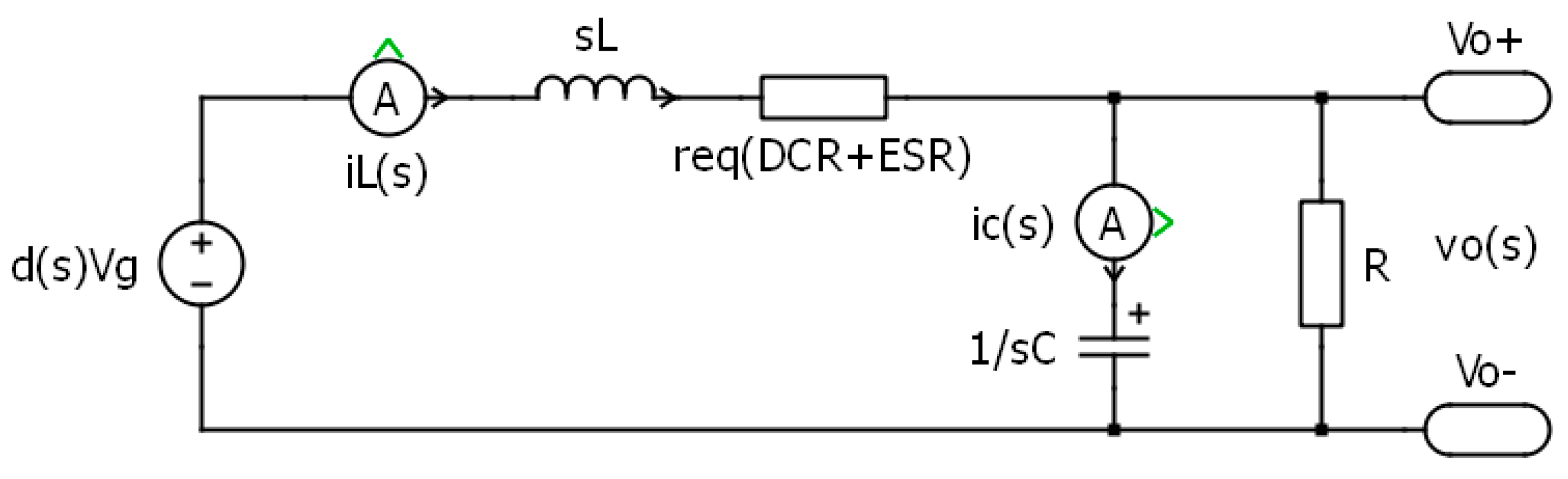
2.2. Small Signal Modeling of Open Loop Buck Converters
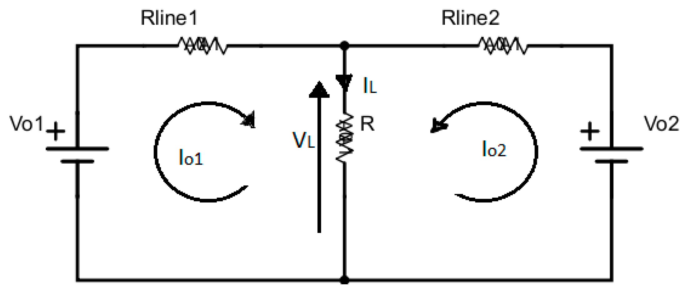
2.3. Issues in Parallel Connected Converters
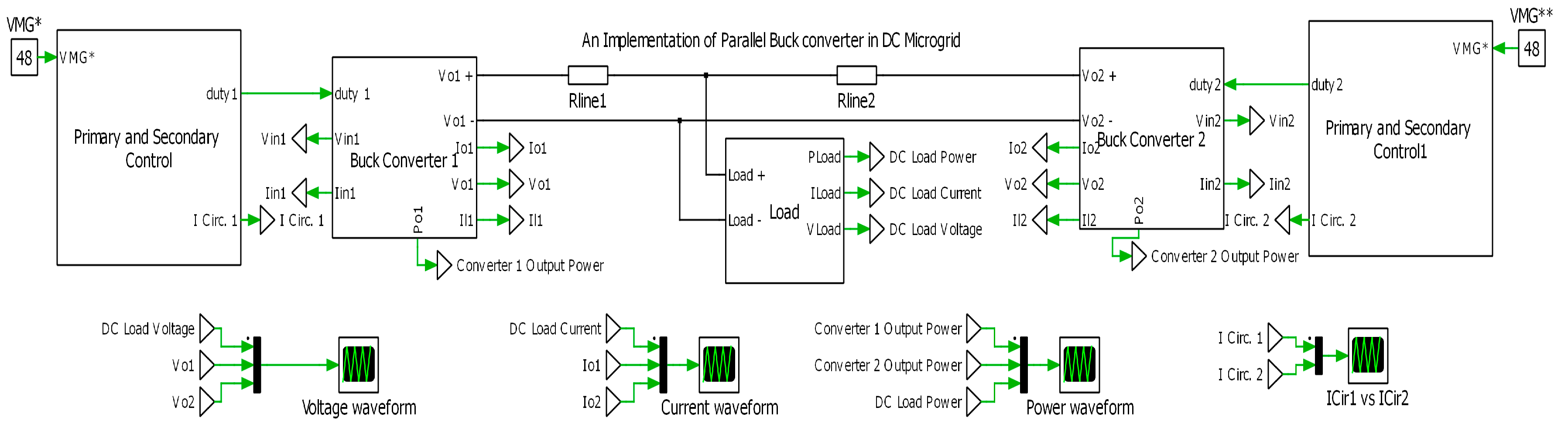
3. Primary and Secondary Control Design in Current Control Mode
3.1. Primary Control Design
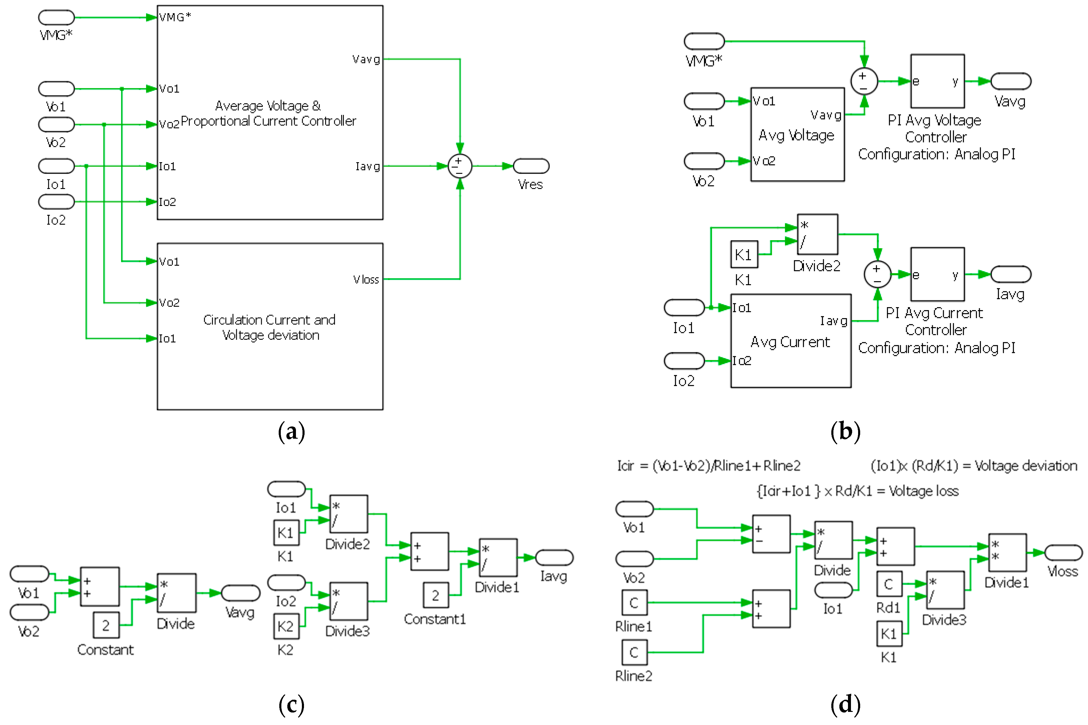
3.2. Secondary Control Design
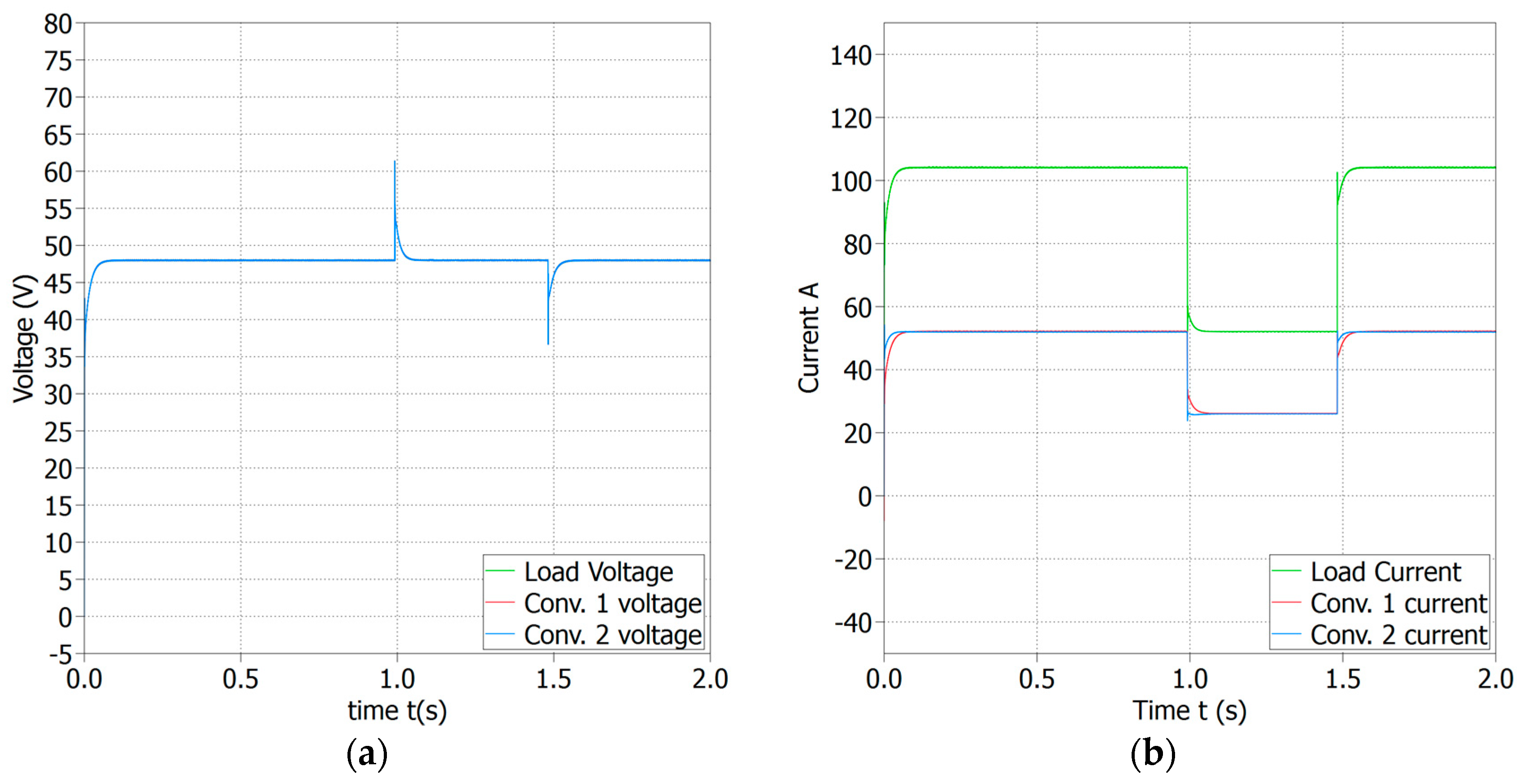
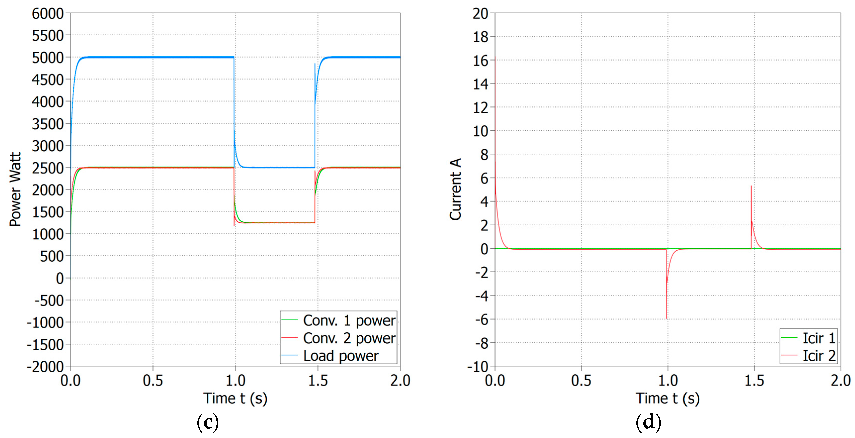
4. The Simulation Results and Discussion
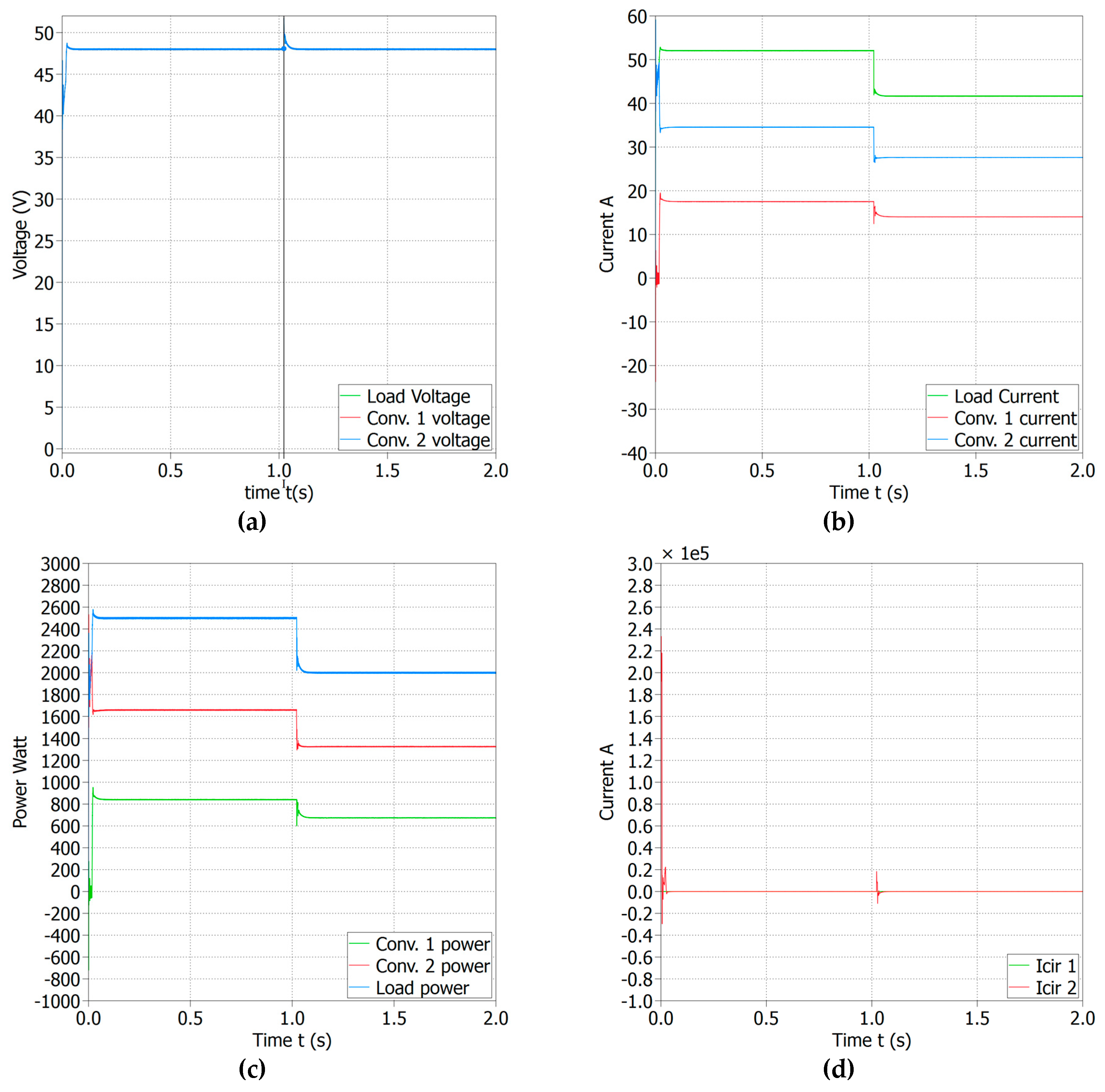
4.1. Scenario 1
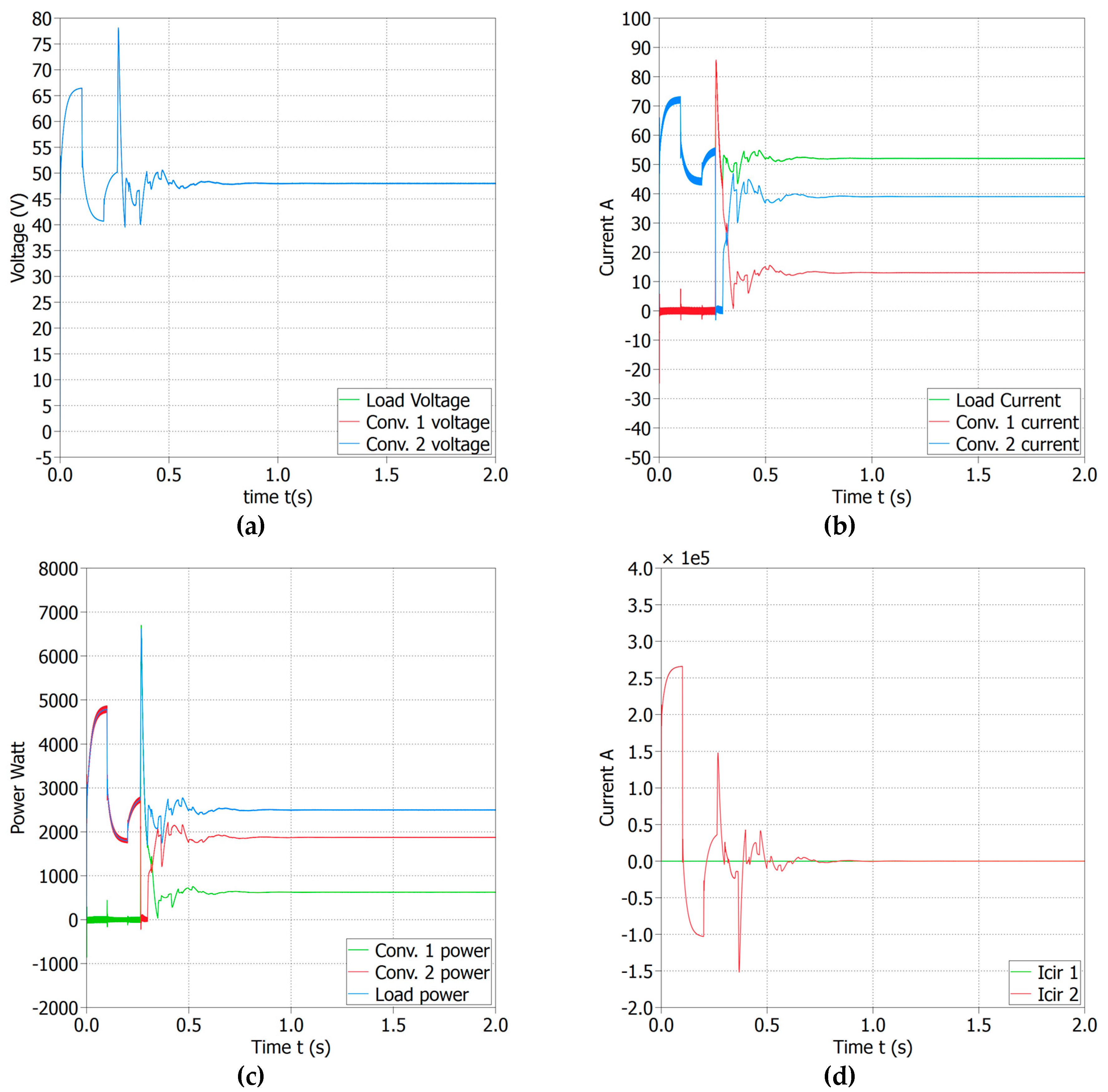
4.2. Scenario 2
4.3. Scenario 3
5. Conclusions
Author Contributions
Funding
Conflicts of Interest
References
- Zhou, X.; Guo, T.; Ma, Y. An overview on microgrid technology. In Proceedings of the IEEE International Conference on Mechatronics and Automation, Beijing, China, 2–5 August 2015; pp. 76–81. [Google Scholar]
- Zhou, X.; Cui, L.; Ma, Y. Research on smart grid technology. In Proceedings of the International Conference on Computer Application and System Modeling, Taiyuan, China, 22–24 October 2010; pp. 599–603. [Google Scholar]
- Zhang, C.; Wu, J.; Zhou, Y.; Cheng, M.; Long, C. Peer-to-Peer energy trading in a Microgrid. Applied Energy 2018, 220, 1–12. [Google Scholar] [CrossRef]
- Jogunola, O.; Ikpehai, A.; Anoh, K.; Adebisi, B.; Hammoudeh, M.; Gacanin, H.; Harris, G. Comparative analysis of P2P architectures for energy trading and sharing. Energies 2017, 11, 62. [Google Scholar] [CrossRef]
- Guerrero, J.M.; Vasquez, J.C.; Matas, J.; De Vicuña, L.G.; Castilla, M. Hierarchical control of droop-controlled AC and DC microgrids—A general approach toward standardization. IEEE Trans. Ind. Electron. 2011, 58, 158–172. [Google Scholar] [CrossRef]
- Unamuno, E.; Barrena, J.A. Equivalence of primary control strategies for AC and DC microgrids. Energies 2017, 10, 91. [Google Scholar] [CrossRef]
- Kumar, D.; Zare, F.; Ghosh, A. DC microgrid technology: System architectures, AC grid interfaces, grounding schemes, power quality, communication networks, applications and standardizations aspects. IEEE Access 2017, 5, 12230–12256. [Google Scholar] [CrossRef]
- Lonkar, M.; Ponnaluri, S. An overview of DC microgrid operation and control. In Proceedings of the 2015 Sixth International Renewable Energy Congress (IREC), Sousse, Tunisia, 24–26 March 2015. [Google Scholar]
- Meng, L.; Shafiee, Q.; Ferrari-Trecate, G.; Karimi, H.; Fulwan, D.; Lu, X.; Zapata, J.M.G. Review on Control Methods of DC Microgrid. IEEE J. Emerg. Sel. Top. Power Electron. 2017, 5, 928–948. [Google Scholar]
- Sahoo, S.K.; Sinha, A.K.; Kishore, N.K. Control techniques in AC, DC, and Hybrid AC–DC Microgrid: A review. IEEE J. Emerg. Sel. Top. Power Electron. 2018, 6, 738–759. [Google Scholar] [CrossRef]
- Thomas, R.M.; Jose, D. Control method for Parallel DC-DC converters used in standalone Photovoltaic power Systems. Int. J. Energy Res. Technol. 2015, 4, 784–789. [Google Scholar]
- Babu, J.; Mathew, B.K. Decentralized Control Method for load sharing and circulating current minimizaion in standalone DC Microgrid. Int. J. Adv. Res. Electr. Electron. Instrum. Eng. 2016, 5, 7170–7178. [Google Scholar]
- Braitor, A.C.; Konstantopoulos, G.C.; Kadirkamanathan, V. Power sharing of parallel operated DC-DC converters using current-limiting droop control. In Proceedings of the 25th Mediterranean Conference on Control and Automation (MED), Valletta, Malta, 3–6 July 2017. [Google Scholar]
- Shahid, M.; Khan, M.; Hashmi, K.; Habib, S.; Jiang, H.; Tang, H. A control methodology for load sharing system restoration in islanded DC micro grid with faulty communication links. Electronics 2018, 7, 90. [Google Scholar] [CrossRef]
- Lu, X.; Guerrero, J.M.; Sun, K. Distributed secondary control for dc microgrid applications with enhanced current sharing accuracy. In Proceedings of the 2013 IEEE International Symposium on Industrial Electronics, Taipei, Taiwan, 28–31 May 2013. [Google Scholar]
- Liu, X.K.; He, H.; Wang, Y.W.; Xu, Q.; Guo, F. Distributed Hybrid Secondary Control for a DC Microgrid via Discrete-Time Interaction. IEEE Trans. Energy Convers. 2018, 33, 1865–1875. [Google Scholar] [CrossRef]
- Zammit, D.; Staines, C.S.; Apap, M.; Micallef, A. Paralleling of buck converters for DC microgrid operation. In Proceedings of the IEEE-3rd International Conference on Control, Decision and Information Technologies, Saint Julian’s, Malta, 6–8 April 2016. [Google Scholar]
- Gunasekaran, M.; Mohamed Ismail, H.; Chokkalingam, B.; Mihet-Popa, L.; Padmanaban, S. Energy Management Strategy for Rural Communities’ DC Micro Grid Power System Structure with Maximum Penetration of Renewable Energy Sources. Appl. Sci. 2018, 8, 585. [Google Scholar] [CrossRef]
- Phurailatpam, C.; Sangral, R.; Rajpurohit, B.S.; Singh, S.N.; Longatt, F.G. Design and analysis of a dc microgrid with centralized battery energy storage system. In Proceedings of the 2015 Annual IEEE India Conference (INDICON), New Delhi, India, 17–20 December 2015. [Google Scholar]
- Khoucha, F.; Benbouzid, M.; Amirat, Y.; Kheloui, A. Integrated energy management of a plug-in electric vehicle in residential distribution systems with renewables. In Proceedings of the 24th IEEE International Symposium on Industrial Electronics, Búzios, Rio de Janeiro, Brazil, 3–5 June 2015. [Google Scholar]
- Wang, H.; Han, M.; Guerrero, J.M.; Vasquez, J.C.; Teshager, B.G. Distributed secondary and tertiary controls for I–V droop-controlled-paralleled DC–DC converters. IET Gener. Transm. Distrib. 2017, 12, 1538–1546. [Google Scholar] [CrossRef]
- Kato, M.; Imura, T.; Hori, Y. Study on maximize efficiency by secondary side control using DC-DC converter in wireless power transfer via magnetic resonant coupling. World Electr. Veh. J. 2013, 6, 858–862. [Google Scholar] [CrossRef]
- Zhong, W.; Huang, Z.; Zhu, T.; Gu, Y.; Zhang, Q.; Yi, P.; Jiang, D.; Xiao, S. IDES: Incentive-driven distributed energy sharing in sustainable microgrids. In Proceedings of the International Green Computing Conference (IGCC), Dallas, TX, USA, 3–5 November 2014. [Google Scholar]
- Luo, F.L.; Ye, H. Small signal analysis of energy factor and mathematical modeling for power dc–dc converters. IEEE Trans. Power Electron. 2007, 22, 69–79. [Google Scholar] [CrossRef]
- Wang, F.; Ma, K. Transfer function modeling and analysis of the open-loop Buck converter using the fractional calculus. Chin. Phys. B 2013, 22, 030506. [Google Scholar] [CrossRef]
- Luo, F.; Ye, H.; Muhammad, R. Digital Power Electronics and Operation; Elsevier Academic Press: San Diego, CA, USA, 2005. [Google Scholar]
- Salem, F.A.; Rashed, A.A. PID controllers and algorithms: Selection and design techniques applied in mechatronics systems design-Part II. Int. J. Eng. Sci. 2013, 2, 191–203. [Google Scholar]


| Parameters | Values |
|---|---|
| Input voltage Vg | 100 V |
| Output voltage Vo | 48 V |
| Switching frequency | 10 kHz |
| Converter capacity | 2.5 kW |
| Inductor | 0.479 mH |
| Capacitor | 271.25 μF |
| ESR | 0.03 Ω |
| DCR | 0.002 Ω |
| Percentage peak to peak ripple inductor current | 10% |
| Percentage peak ripple output voltage ΔV0 | 0.5% |
| Parameters | Formulae |
|---|---|
| R | ; 7.5 < R < 10 |
| K | |
| Parameters | Values |
|---|---|
| Simulation Time t | 2 s |
| Communication delay | 0~100 ms |
| Current proportion of converter 1 K1 | 1 |
| Current proportion of converter 2 K2 | 1~4 |
| Inner current controller Ki | 0.993 |
| Inner current controller Kp | 790 |
| Outer voltage controller Ki | 0.077 |
| Outer voltage controller Kp | 5.7 |
| Avg. voltage controller Ki of converter 1 | 0.05 |
| Avg. voltage controller Kp of converter 1 | 50 |
| Avg. current controller Ki of converter 1 | 90 |
| Avg. current controller Kp of converter 1 | 0.002 |
| Avg. voltage controller Ki of converter 2 | 58 |
| Avg. voltage controller Kp of converter 2 | 0.009 |
| Avg. current controller Ki of converter 2 | 0.9 |
| Avg. current controller Kp of converter 2 | 0.01 |
© 2019 by the authors. Licensee MDPI, Basel, Switzerland. This article is an open access article distributed under the terms and conditions of the Creative Commons Attribution (CC BY) license (http://creativecommons.org/licenses/by/4.0/).
Share and Cite
Ali, S.; Shengxue, T.; Jianyu, Z.; Ali, A.; Nawaz, A. An Implementation of Parallel Buck Converters for Common Load Sharing in DC Microgrid. Information 2019, 10, 91. https://doi.org/10.3390/info10030091
Ali S, Shengxue T, Jianyu Z, Ali A, Nawaz A. An Implementation of Parallel Buck Converters for Common Load Sharing in DC Microgrid. Information. 2019; 10(3):91. https://doi.org/10.3390/info10030091
Chicago/Turabian StyleAli, Sikander, Tang Shengxue, Zhang Jianyu, Ahmad Ali, and Arshad Nawaz. 2019. "An Implementation of Parallel Buck Converters for Common Load Sharing in DC Microgrid" Information 10, no. 3: 91. https://doi.org/10.3390/info10030091