
Fabrication of Suspended PMMA-Graphene Membrane for High Sensitivity LC-MEMS Pressure Sensor

 , ,
, ,  , and
, and
Abstract
:1. Introduction
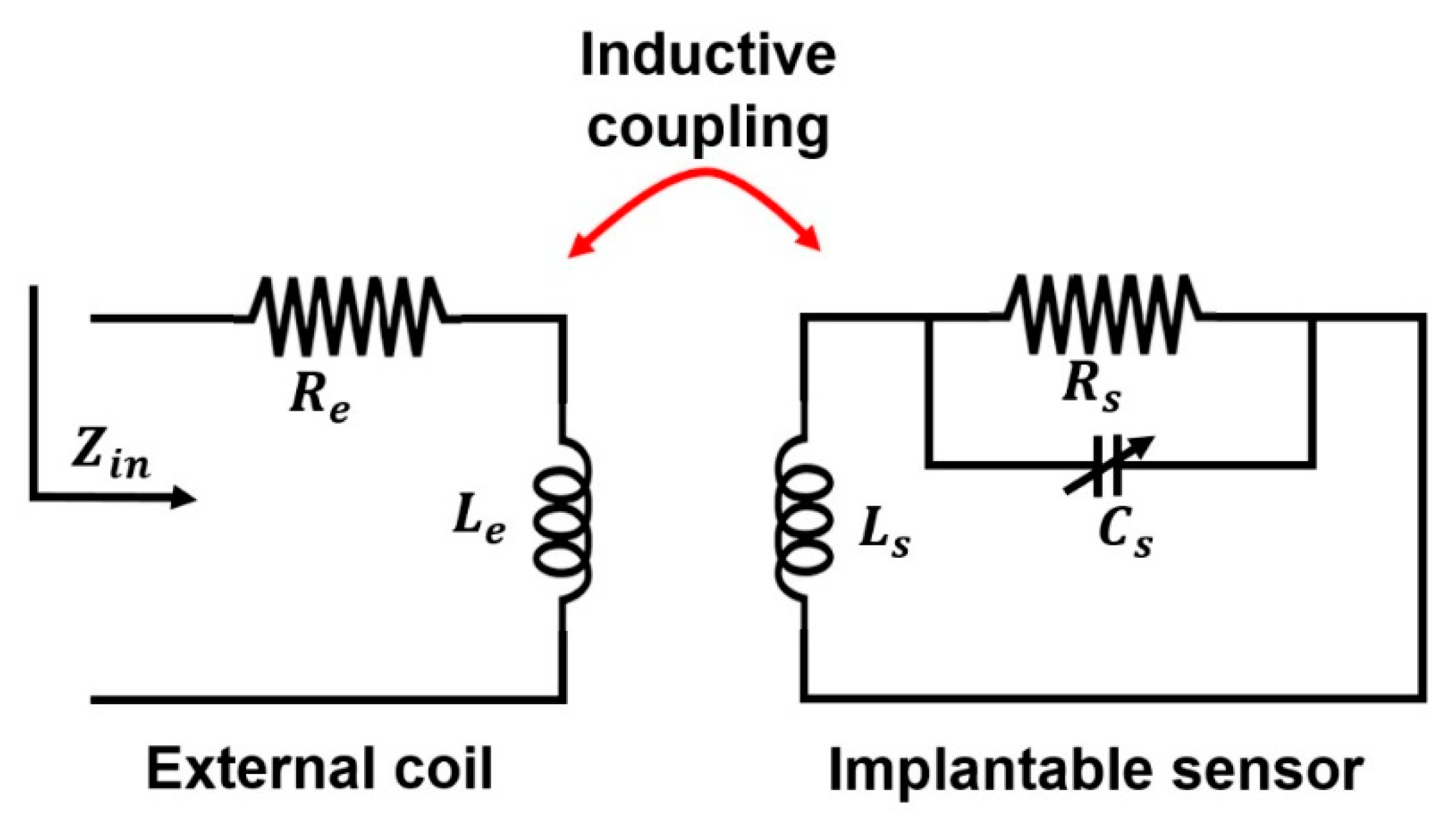
2. LC-MEMS Pressure Sensor Working Principle
3. Methodology
4. Results and Discussion
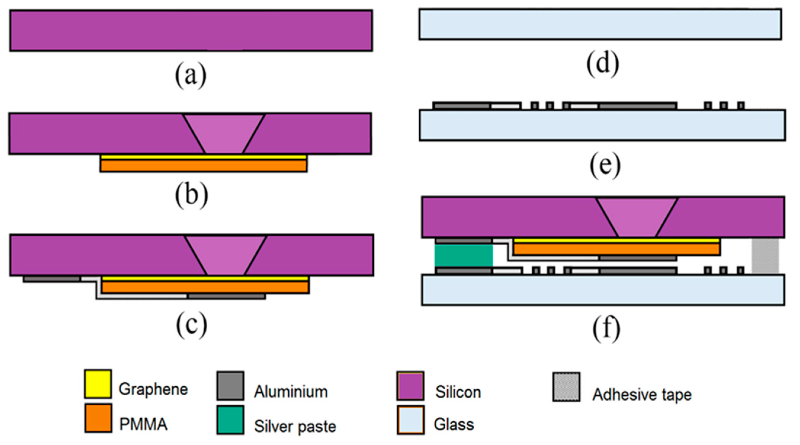
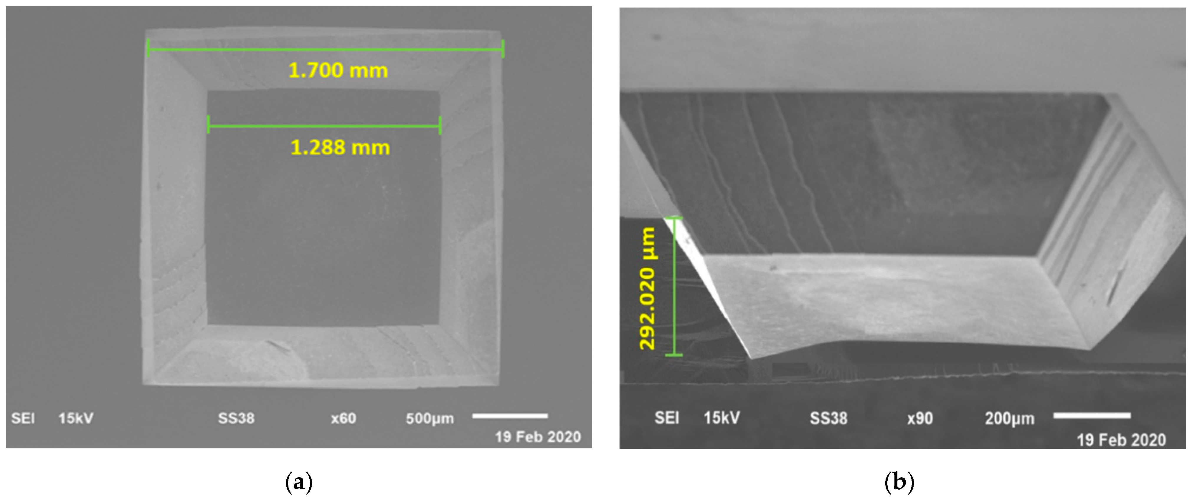
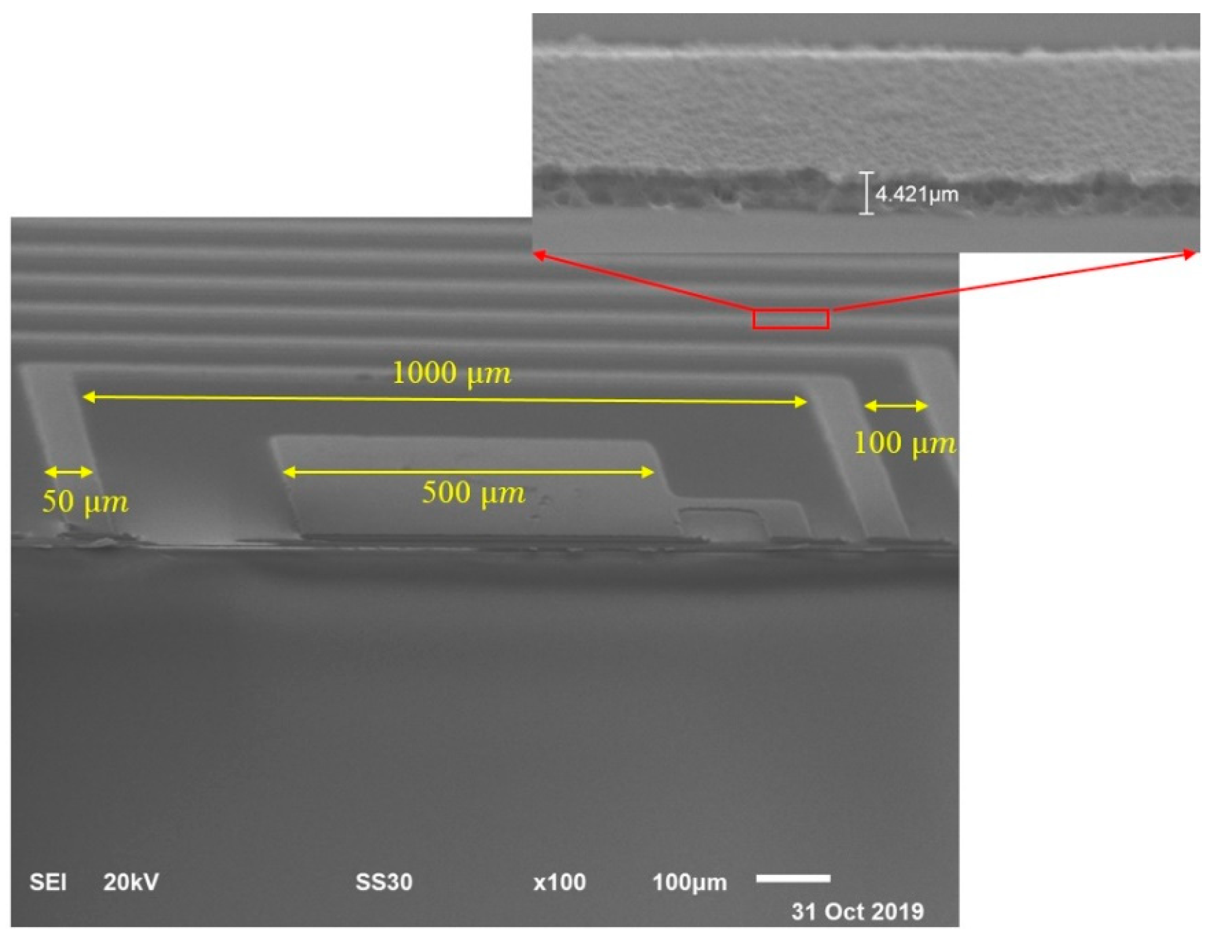
4.1. Fabrication of Silicon Trench
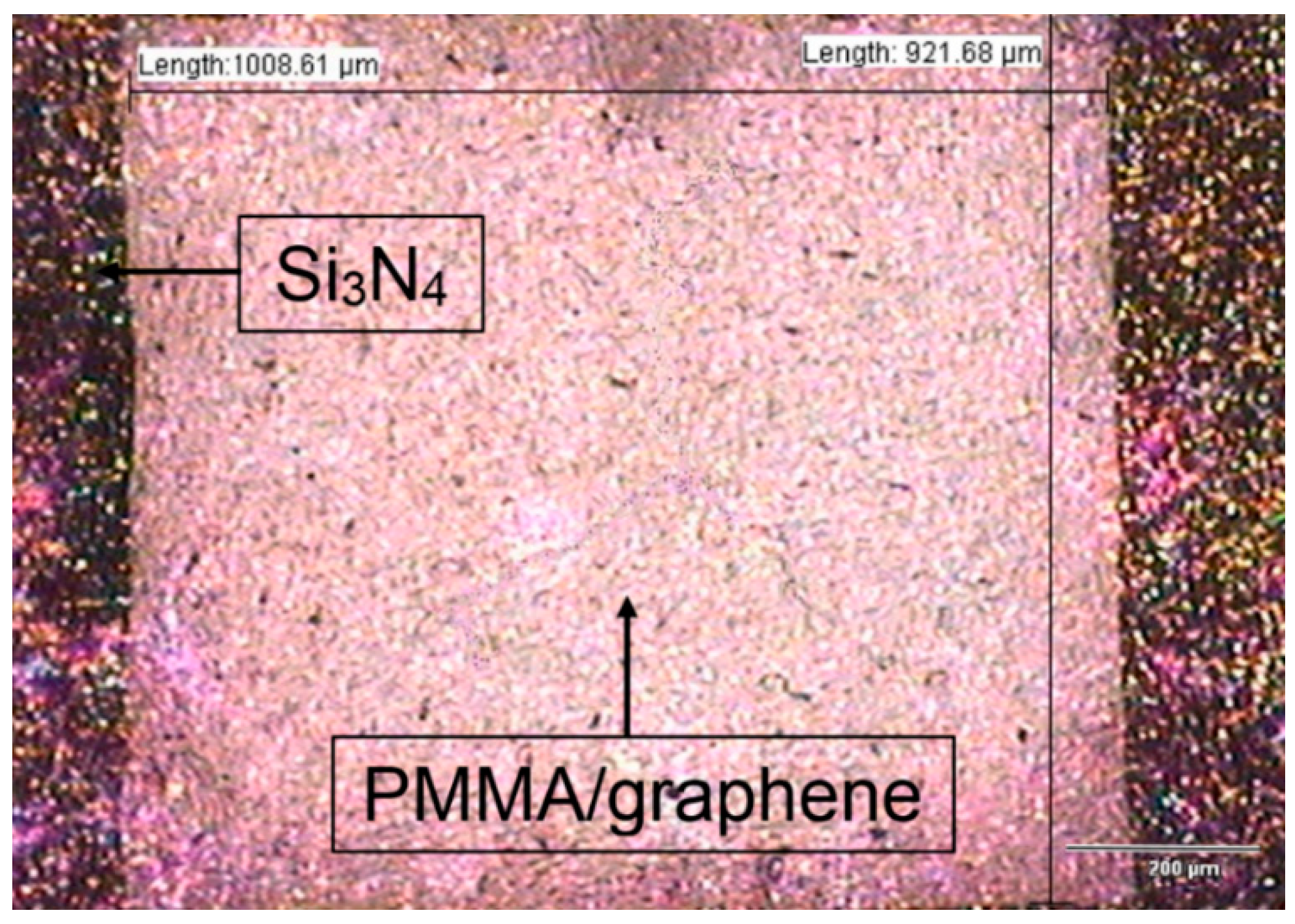
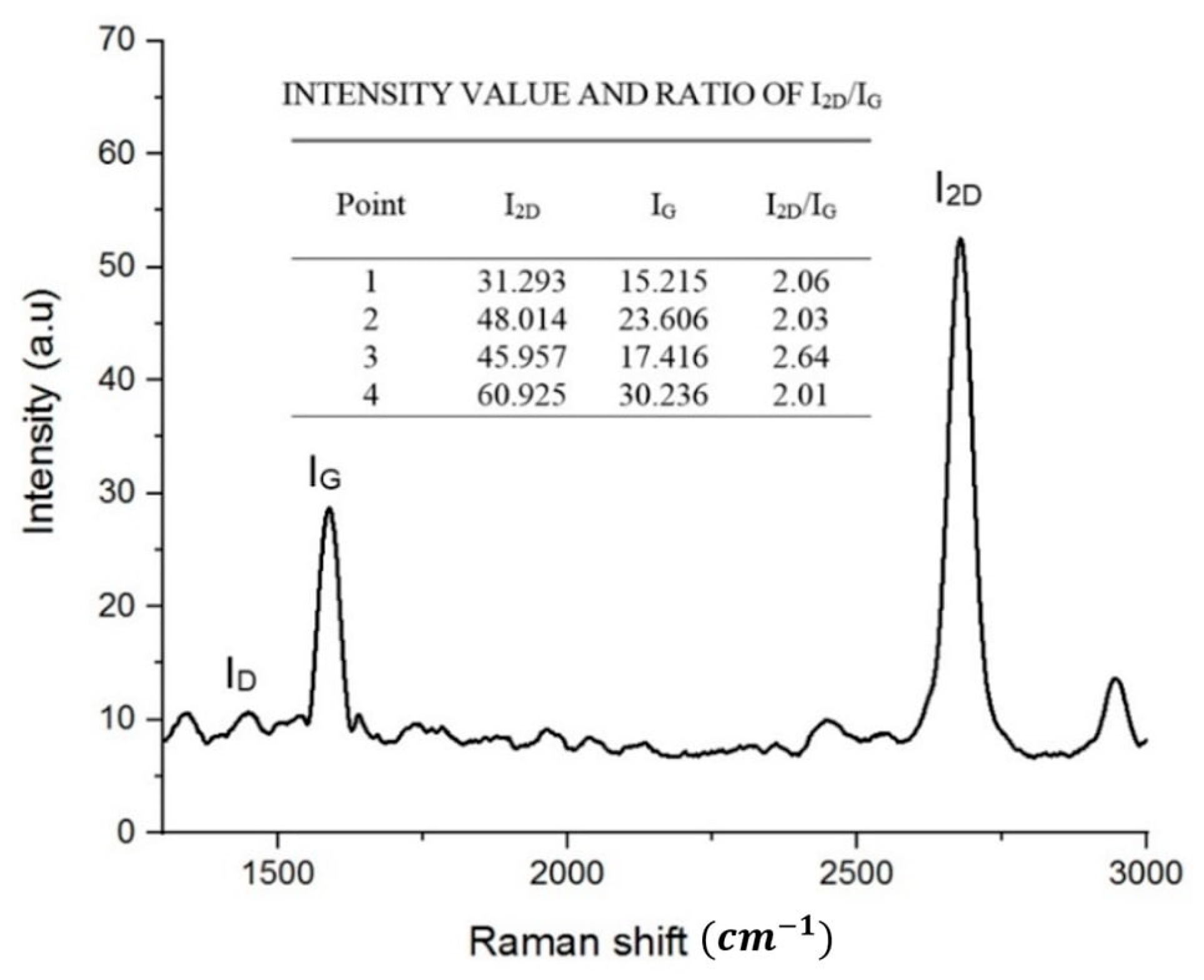
4.2. Development and Characterization of Suspended PMMA/Graphene
4.3. Development and Characterization of Planar Microcoil
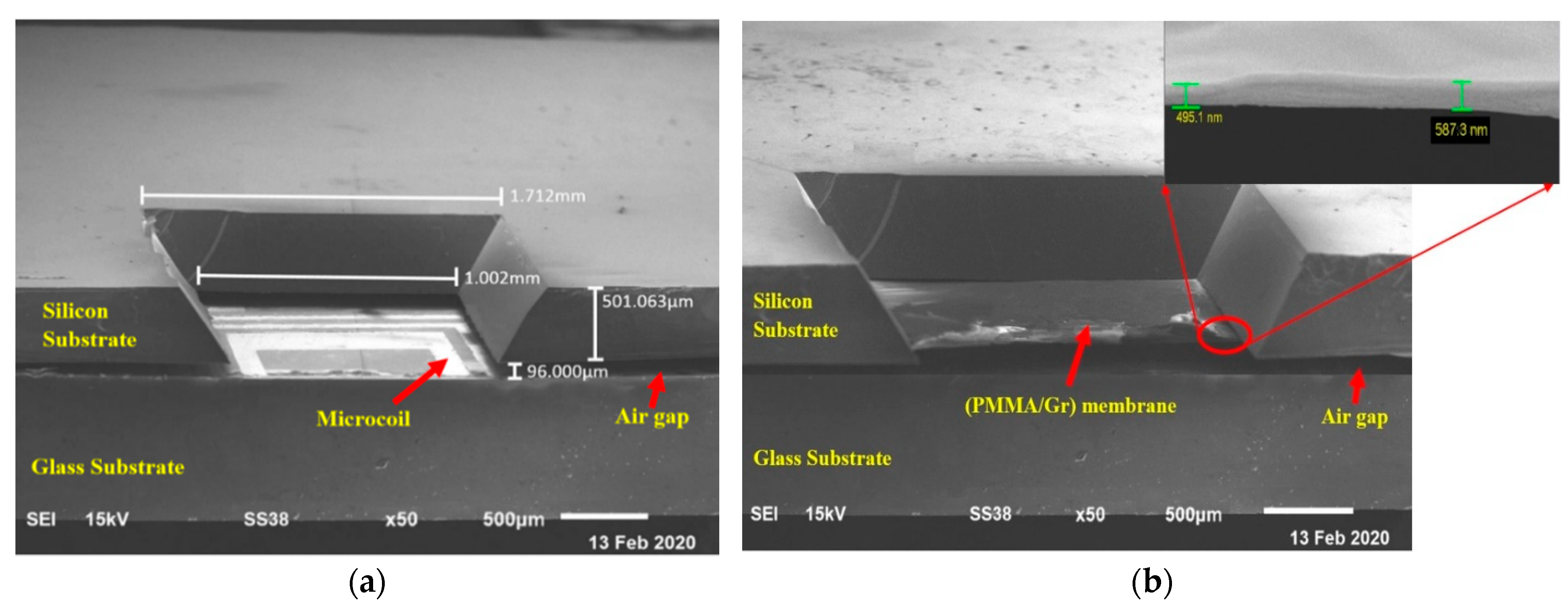
4.4. Completed Structure of LC-MEMS Pressure Sensor
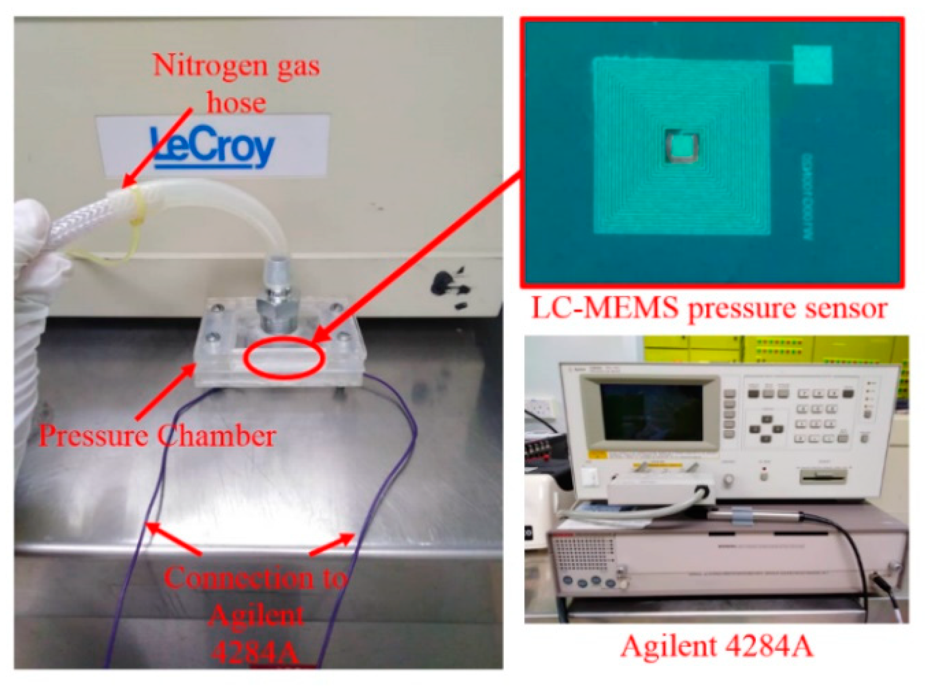
4.5. Low-Pressure Testing of LC-MEMS Pressure Sensor
5. Conclusions
Author Contributions
Funding
Institutional Review Board Statement
Data Availability Statement
Acknowledgments
Conflicts of Interest
References
- Cui, J.; Zhang, B.; Duan, J.; Guo, H.; Tang, J. A micro-pressure sensing method based on the micropatterned electrodes filled with the microspheres. Materials 2017, 10, 1439. [Google Scholar] [CrossRef] [PubMed] [Green Version]
- Mitrakos, V.; Macintyre, L.; Denison, F.C.; Hands, P.J.W.; Desmulliez, M.P.Y. Design, manufacture and testing of capacitive pressure sensors for low-pressure measurement ranges. Micromachines 2017, 8, 41. [Google Scholar] [CrossRef] [Green Version]
- Dinh, T.H.N.; Martincic, E.; Dufour-Gergam, E.; Joubert, P.Y. Mechanical characterization of PDMS films for the optimization of polymer based flexible capacitive pressure microsensors. J. Sens. 2017, 2017, 8235729. [Google Scholar] [CrossRef]
- Berger, C.; Phillips, R.; Pasternak, I.; Sobieski, J.; Strupinski, W.; Vijayaraghavan, A. Touch-mode capacitive pressure sensor with graphene-polymer heterostructure membrane. 2D Mater. 2018, 5, 015025. [Google Scholar] [CrossRef]
- Woo, S.T.; Han, J.-H.; Lee, J.H.; Cho, S.; Seong, K.-W.; Choi, M.; Cho, J.-H. Realization of a high sensitivity microphone for a hearing aid using a graphene−PMMA laminated diaphragm. ACS Appl. Mater. Interfaces 2017, 9, 1237–1246. [Google Scholar] [CrossRef]
- Koley, G.; Liu, J.; Nomani, M.W.; Yim, M.; Wen, X.; Hsia, T.Y. Miniaturized implantable pressure and oxygen sensors based on polydimethylsiloxane thin films. Mater. Sci. Eng. C 2009, 29, 685–690. [Google Scholar] [CrossRef] [PubMed] [Green Version]
- Xue, N.; Chang, S.; Lee, J.B. A SU-8-based microfabricated implantable inductively coupled passive RF wireless intraocular pressure sensor. J. Microeletromech. Syst. 2012, 21, 1338–1346. [Google Scholar] [CrossRef]
- Bais, B.; Yusof, N.; Soin, N.; Yunas, J.; Majlis, B.Y. Development and characterization of freestanding poly(methyl methacrylate)/monolayer graphene membrane. IEEE Access 2020, 8, 29702–29710. [Google Scholar] [CrossRef]
- Lau, C.N.; Bao, W.; Velasco, J. Properties of suspended graphene membranes. Mater. Today 2012, 15, 238–245. [Google Scholar] [CrossRef]
- Akiwande, D.; Brennan, C.J.; Bunch, J.S.; Egberts, P.; Felts, J.R.; Gao, H.; Huang, R.; Kim, J.S.; Li, T.; Li., Y.; et al. A review on mechanics and mechanical properties of 2D materials—Graphene and beyond. Extrem. Mech. Lett. 2017, 13, 42–77. [Google Scholar] [CrossRef] [Green Version]
- Berger, C.; Phillips, R.; Centeno, A.; Zurutuza, A.; Vijayaraghavan, A. Capacitive pressure sensing with suspended graphene-polymer heterostructure membranes. Nanoscale 2017, 9, 17439–17449. [Google Scholar] [CrossRef] [Green Version]
- Dash, S.; Patnaik, A. Impact of silicon-based substrates on graphene THz antenna. Phys. E Low-Dimens. Syst. Nanostruct. 2021, 126, 114479. [Google Scholar] [CrossRef]
- Bunch, J.S.; Dunn, M.L. Adhesion mechanics of graphene membranes. Solid State Commun. 2021, 152, 1359–1364. [Google Scholar] [CrossRef] [Green Version]
- Kou, H.; Zhang, L.; Tan, Q.; Liu, G.; Dong, H.; Zhang, W.; Xiong, J. Wireless wide-range pressure sensor based on graphene/PDMS sponge for tactile monitoring. Sci. Rep. 2019, 9, 3916. [Google Scholar] [CrossRef]
- Cheng, L.; Wang, R.; Hao, X.; Liu, G. Design of flexible pressure sensor based on conical microstructure PDMS-bilayer graphene. Sensors 2021, 21, 289. [Google Scholar] [CrossRef]
- Huang, Q.; Dong, L.; Wang, L. LC Passive wireless sensors toward a wireless sensing platform: Status, prospect, and challenges. J. Microelectromech. Syst. 2016, 25, 822–841. [Google Scholar] [CrossRef]
- Zhai, J.; How, T.V.; Hon, B. Design and modelling of a passive wireless pressure sensor. CIRP Ann. Manuf. Technol. 2010, 59, 187–190. [Google Scholar] [CrossRef]
- Hu, S.; Chen, H.; Jia, S.; Xiao, X.; Cao, Y.; Wang, W. A wireless passive extra-arterial implantable blood pressure monitoring sensing system for rats. Microsyst. Technol. 2021, 27, 2595–2603. [Google Scholar] [CrossRef]
- De Santis, I.; Cacciotti, M. Wireless Implantable implantable and biodegradable sensors for postsurgery monitoring: Current status and future perspectives. Nanotechnology 2020, 31, 1–47. [Google Scholar] [CrossRef] [PubMed]
- Chitnis, G.; Maleki, T.; Samuels, B.; Cantor, L.B.; Ziaie, B. A minimally invasive implantable wireless pressure sensor for continuous IOP monitoring. IEEE Trans. Biomed. Eng. 2013, 60, 250–256. [Google Scholar] [CrossRef] [PubMed]
- Lee, H.Y.; Choi, B.; Kim, S.; Kim, S.J.; Bae, W.J.; Kim, S.W. Sensitivity-enhanced LC pressure sensor for wireless bladder pressure monitoring. IEEE Sens. J. 2016, 16, 4715–4724. [Google Scholar] [CrossRef]
- Benken, A.; Gianchandani, Y. Passive wireless pressure sensing for gastric manometry. Micromachines 2019, 10, 868. [Google Scholar] [CrossRef] [Green Version]
- Weaver, J.N.; Alspaugh, J.C.; Behkam, B. Toward a minimally invasive bladder pressure monitoring system: Model bladder for in vitro testing. In Proceedings of the 3rd IEEE RAS EMBS International Conference on Biomedical Robotics and Biomechatronics, Tokyo, Japan, 26–29 September 2010; pp. 638–643. [Google Scholar]
- Dakurah, M.N.; Koo, C.; Choi, W.; Joung, Y.H. Implantable bladder sensors: A methodological review. Int. Neurourol. J. 2015, 19, 133–141. [Google Scholar] [CrossRef] [Green Version]
- Li, Y.; Zhao, M.; Wei, Q.; Yu, J.; Chen, J.; Chen, D.; Wang, J. Wireless passive intracranial pressure sensor based on vacuum packaging. IEEE Sens. J. 2020, 20, 11247–11255. [Google Scholar] [CrossRef]
- Yu, L.; Kim, B.J.; Meng, E. Chronically implanted pressure sensors: Challenges and state of the field. Sensors 2014, 14, 20620–20644. [Google Scholar] [CrossRef] [Green Version]
- Luo, M.; Martinez, A.W.; Song, C.; Herrault, F.; Allen, M.G. A microfabricated wireless RF pressure sensor made completely of biodegradable materials. J. Microelectromech. Syst. 2014, 23, 4–13. [Google Scholar] [CrossRef]
- Farooq, M.; Iqbal, T.; Vazquez, P.; Farid, N.; Thampi, S.; Wijns, W.; Shahzad, A. Thin-film flexible wireless pressure sensor for continuous pressure monitoring in medical applications. Sensors 2020, 20, 6653. [Google Scholar] [CrossRef]
- Peng, Y.; Wang, T.; Jiang, W.; Liu, X.; Wen, X.; Wang, G. Modeling and optimization of inductively coupled wireless bio-pressure sensor system using the design of experiments method. IEEE Trans. Compon. Packag. Manuf. Technol. 2018, 8, 65–72. [Google Scholar] [CrossRef]
- Yang, X.; Wang, Y.; Qing, X. A flexible capacitive pressure sensor based on ionic liquid. Sensors 2018, 18, 2395. [Google Scholar] [CrossRef] [Green Version]
- Burham, N.; Hamzah, A.A.; Yunas, J.; Majlis, B.Y. Electrochemically etched nanoporous silicon membrane for separation of biological molecules in mixture. J. Micromech. Microeng. 2017, 27, 075021. [Google Scholar] [CrossRef]
- Yusof, N.; Bais, B.; Majlis, B.Y.; Soin, N.; Yunas, J. Optimization of KOH etching process for MEMS square diaphragm using response surface method. Indones. J. Electr. Eng. Comput. Sci. 2019, 15, 113. [Google Scholar] [CrossRef]
- Abidin, U.; Majlis, B.Y.; Yunas, J. Fabrication of pyramidal cavity structure with micron-sized tip using anisotropic KOH etching of silicon (100). J. Teknol. 2015, 74, 137–148. [Google Scholar] [CrossRef] [Green Version]
- Pal, P.; Sato, K. A comprehensive review on convex and concave corners in silicon bulk micromachining based on anisotropic wet chemical etching. Micro Nano Syst. Lett. 2015, 3, 6. [Google Scholar] [CrossRef] [Green Version]
- Nair, R.R.; Blake, P.; Grigorenko, A.N.; Novoselov, K.S.; Booth, T.J.; Stauber, T.; Peres, N.M.R.; Geim, A.K. Fine structure constant defines visual transparency of graphene. Science 2018, 320, 1308. [Google Scholar] [CrossRef] [PubMed] [Green Version]
- Ni, Z.H.; Yu, T.; Lu, Y.H.; Wang, Y.Y.; Feng, Y.P.; Shen, Z.X. Uniaxial strain on graphene: Raman spectroscopy study and band-gap opening. ACS Nano 2008, 2, 2301–2305. [Google Scholar] [CrossRef] [PubMed]
- Smith, A.D.; Vaziri, S.; Niklausa, F.; Fischer, A.C.; Sterner, M.; Delin, A.; Östling, M.; Lemme, M.C. Pressure sensors based on suspended graphene membranes. Solid-State Electron. 2013, 88, 89–94. [Google Scholar] [CrossRef]
- Ferrari, A.C.; Meyer, J.C.; Scardaci, V.; Casiraghi, C.; Lazzeri, M.; Mauri, F.; Geim, A.K. Raman spectrum of graphene and graphene layers. Phys. Rev. Lett. 2006, 97, 187401. [Google Scholar] [CrossRef] [PubMed] [Green Version]
- Tang, B.; Guoxin, H.; Gao, H. Raman spectroscopic characterization of graphene. Appl. Spectrosc. Rev. 2010, 45, 369–4070. [Google Scholar] [CrossRef]
- Nguyen, V.T.; Le, H.D.; Nguyen, V.C.; Ngo, T.T.T.; Le, D.Q.; Nguyen, X.N.; Phan, N.M. Synthesis of multi-layer graphene films on copper tape by atmospheric pressure chemical vapor deposition method. Adv. Nat. Sci. Nanosci. Nanotechnol. 2013, 4, 035012. [Google Scholar] [CrossRef]


| Parameter | Value |
|---|---|
| Pressure range | 0–75 mmHg (normal) ~150 mmHg (abnormal) [26] |
| Frequency response | 10–100 MHz [27] |
| Size | 8 mm × 8 mm [16] |
| Sensor sensitivity | 2–162 kHz/mmHg [16,17,18,19,20,21,22,25,28] |
| Parameter | Characteristics |
|---|---|
| Membrane’s material | (PMMA/Gr) |
| Membrane’s thickness (PMMA/Gr) | 0.5 µm |
| Membrane’s area | 1.0 mm × 1.0 mm |
| Sensor’s size | 8 mm |
| Air gap | 96 µm |
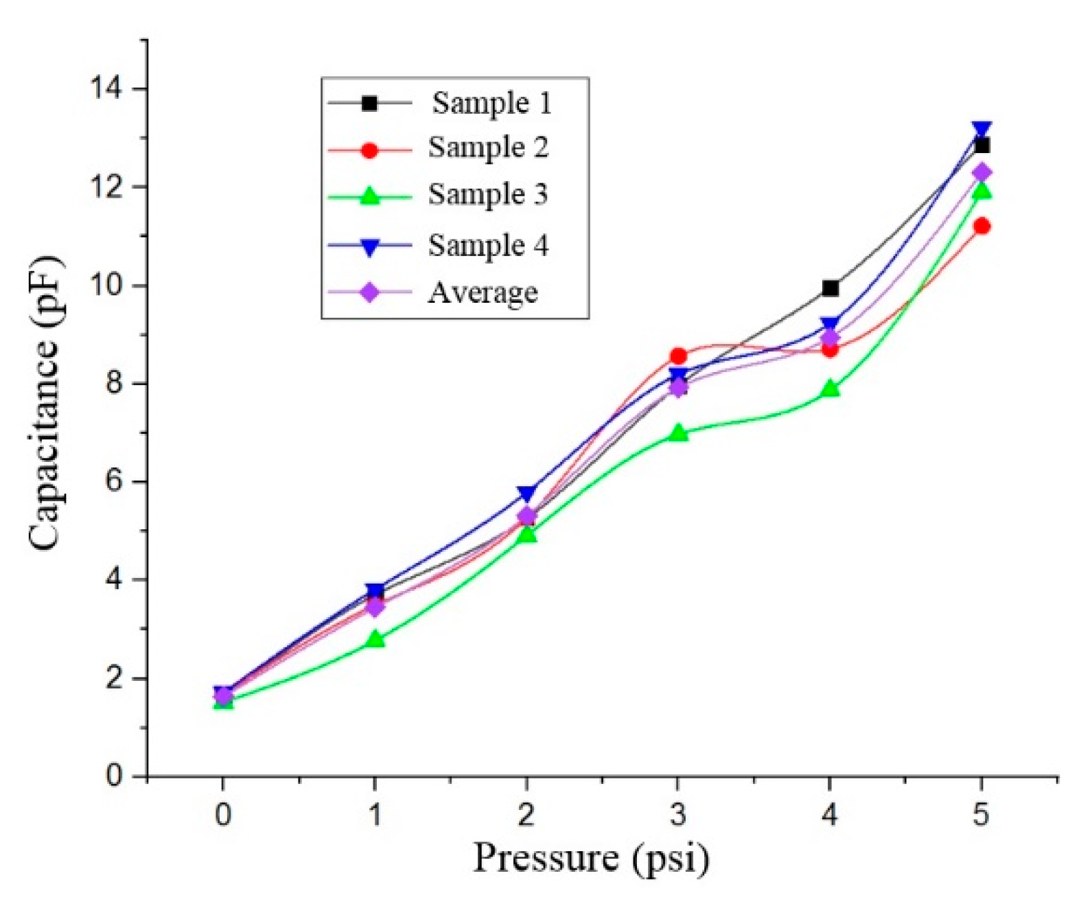
| Capacitance changes | 1.64–12.32 pF |
| Microcoil’s inductance | 2.49 µH |
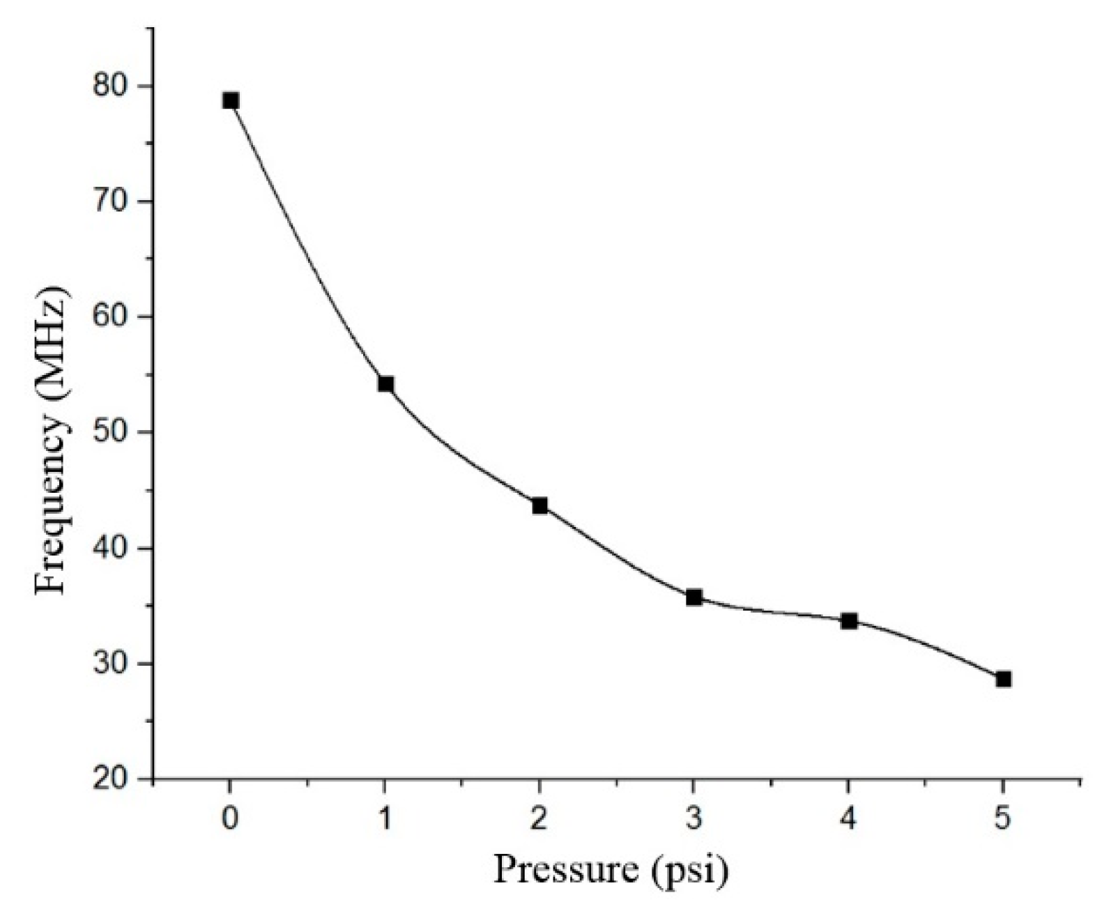
| Frequency changes | 28.74–78.76 MHz |
| Quality factor | 21 (at F = 78.76 MHz) |
| Sensor’s sensitivity | 193.45 kHz/mmHg |
Publisher’s Note: MDPI stays neutral with regard to jurisdictional claims in published maps and institutional affiliations. |
© 2021 by the authors. Licensee MDPI, Basel, Switzerland. This article is an open access article distributed under the terms and conditions of the Creative Commons Attribution (CC BY) license (https://creativecommons.org/licenses/by/4.0/).
Share and Cite
Yusof, N.; Bais, B.; Yunas, J.; Soin, N.; Majlis, B.Y. Fabrication of Suspended PMMA-Graphene Membrane for High Sensitivity LC-MEMS Pressure Sensor. Membranes 2021, 11, 996. https://doi.org/10.3390/membranes11120996
Yusof N, Bais B, Yunas J, Soin N, Majlis BY. Fabrication of Suspended PMMA-Graphene Membrane for High Sensitivity LC-MEMS Pressure Sensor. Membranes. 2021; 11(12):996. https://doi.org/10.3390/membranes11120996
Chicago/Turabian StyleYusof, Norliana, Badariah Bais, Jumril Yunas, Norhayati Soin, and Burhanuddin Yeop Majlis. 2021. "Fabrication of Suspended PMMA-Graphene Membrane for High Sensitivity LC-MEMS Pressure Sensor" Membranes 11, no. 12: 996. https://doi.org/10.3390/membranes11120996