Review

Solution-Based Synthesis and Processing of Metal Chalcogenides for Thermoelectric Applications

1
Department of Building, School of Design and Environment, National University of Singapore, 4 Architecture Drive, Singapore 117566, Singapore
2
Institute of Materials Research and Engineering, A*STAR (Agency for Science, Technology and Research), 2 Fusionopolis Way, Innovis, #08-03, Singapore 138634, Singapore
3
Department of Chemistry, National University of Singapore, 3 Science Drive 3, Singapore 117543, Singapore
*
Authors to whom correspondence should be addressed.
Both authors contribute equally to this manuscript.
Appl. Sci. 2019, 9(7), 1511; https://doi.org/10.3390/app9071511
Submission received: 2 March 2019 / Revised: 27 March 2019 / Accepted: 3 April 2019 / Published: 11 April 2019

Abstract

:
Metal chalcogenide materials are current mainstream thermoelectric materials with high conversion efficiency. This review provides an overview of the scalable solution-based methods for controllable synthesis of various nanostructured and thin-film metal chalcogenides, as well as their properties for thermoelectric applications. Furthermore, the state-of-art ink-based processing method for fabrication of thermoelectric generators based on metal chalcogenides is briefly introduced. Finally, the perspective on this field with regard to material production and device development is also commented upon.

Graphical Abstract

1. Introduction

Given the current global energy crisis and environmental issues, the exploitation of green and sustainable resources, such as wind, solar, geothermal, and biomass resources, for energy generation is being extensively developed all over the world. In this context, thermoelectric materials that can directly convert waste heat into electricity have attracted tremendous research interest over the past decades [1,2,3,4]. The thermoelectric conversion efficiency can be conveniently evaluated by the figure of merit ZT = S2σT/κ (where S is the Seebeck coefficient, σ is electrical conductivity, T is absolute temperature, and κ is thermal conductivity). For easy comparison of the electrical and thermal transport properties, the thermal conductivity (κ) and power factor (S2σ) can be used to judge the performance of different thermoelectric materials [5]. Currently, the research in this field is mainly focused on (1) developing novel environmentally benign and naturally abundant thermoelectric materials, (2) improving thermoelectric performance of existing materials through nanostructure engineering, and (3) developing highly efficient modules or devices for practical thermoelectric energy conversion.
Figure 1 summarizes the figure of merit values of current state-of-the-art thermoelectric materials with high conversion efficiency, which are mainly based on metal chalcogenide semiconductors, such as Bi2Te3, Cu2Se, SnSe, and PbTe, etc. [4]. The outstanding ZT values of the metal chalcogenides are mainly ascribed to their relatively weaker covalent bonding strength and higher atomic weight compared to other thermoelectric materials, which lead to low thermal conductivity [6]. The electronic structures and formulations of the chalcogenide materials can be readily engineered through nanotechnology and chemical doping. Moreover, the functional properties of metal chalcogenides can be easily tuned by p-type or n-type doping. Importantly, most of the metal chalcogenide thermoelectric materials are nontoxic, cheap, and Earth-abundant, holding great promise for large-scale production and manipulation.
The practical application of high-performance thermoelectric materials largely relies on the development of scalable synthetic approaches with controllable size, composition, structure, and morphology. The conventional solid-state or gas-phase methodologies are often considered unsatisfactory due to consuming large amounts of energy, harsh reaction conditions, and/or low production rates. Comparatively, solution-based synthesis has been considered to be a powerful and industry-friendly approach for obtaining various metal chalcogenide materials. Currently, there are a number of review papers on metal chalcogenide materials for thermoelectric, photovoltaic, energy storage, electrocatalytic, and photocatalytic applications, some of which involve a specific method for preparation of these materials [6,7,8,9,10,11,12,13,14,15,16,17]. However, there is no comprehensive summary on solution-based synthesis and processing of metal chalcogenide materials for thermoelectric applications. Herein, we will provide an overview on the solution-based synthesis of nanostructured or thin-film metal chalcogenide materials as well as their thermoelectric applications reported recently. We mainly focus on the environmentally benign such materials with high ZT values, such as Bi2Te3, Cu2Se, and SnSe. PbTe is also a high-performance thermoelectric material; however, the environmental concern due to its inherent toxicity limits its large-scale production and application. Other binary and multinary metal chalcogenide materials and their composites are not covered in this paper because of the overwhelming research in this field. Following that, we also introduce the state-of-the-art ink-based processing methods for fabrication of thermoelectric devices based on metal chalcogenides. Finally, we conclude with future prospects of these metal chalcogenide materials for practical thermoelectric applications.

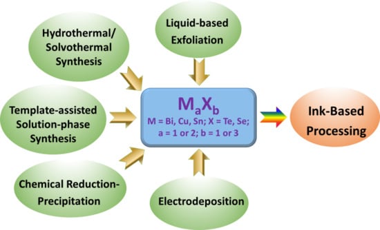
2. Solution-Based Approaches for Synthesis of Metal Chalcogenides

Up to now, several strategies for the preparation of bulk or micro/nanostructured metal chalcogenides have been developed. The traditional solid-state synthesis through reactions among molten states with a specific ratio of solid reactants can generate bulk crystalline metal chalcogenides with high density and symmetry [18,19,20]. However, high temperature (>600 °C) is usually required to overcome the diffusion barriers among the solids in order to achieve an appropriate reaction rate. Kinetic control and mechanism study of these reaction systems are thus rather difficult and also have limited control over the structures coming out of these reactions. The mechanical exfoliation process from high-quality bulk materials can generate pristine single layers of metal chalcogenides with ideal electronic properties [21,22,23]. Nevertheless, the low production yield and small lateral size (typically less than 10 μm) of the exfoliated specimens hamper the practical application of this method. Synthetic approaches based on gas-phase processes such as chemical vapor deposition (CVD) [24,25,26,27] and molecular beam epitaxy growth [28,29] have been successfully applied to produce defectless, uniform thin films of metal chalcogenide materials. However, high-temperature and high-vacuum reaction conditions as well as specific substrates are required for the material growth. The scale-up application of these processes still remains a great challenge due to the low production rate, limited domain size, and difficulty in controlling thickness over the entire substrates.
Recent extensive research suggests that solution-based synthesis is the most feasible method for large-scale production of various metal chalcogenide materials. In a solution-based system, the conditions, such as solvents or surfactants employed, are logically chosen depending on the target metal chalcogenides to be synthesized. The kinetic and thermodynamic parameters can also be easily tuned to alter the speed of nucleation and the formation of the products. In addition, the solution-based synthetic approach does not require extreme conditions such as high temperatures or high pressures, yet it is able to generate products with high yields. In this section, we mainly summarize the solution-based approaches for the controlled synthesis of nanoscaled or thin-film metal chalcogenide materials, including the ‘top-down’ liquid exfoliation method, the ‘bottom-up’ hydrothermal/solvothermal method, and the wet chemical process for construction of nanostructured metal chalcogenides, as well as the electrodeposition method for the formation of both nanoscaled and thin-film materials. The composition, morphology, and properties of these thermoelectric materials are also briefly discussed.

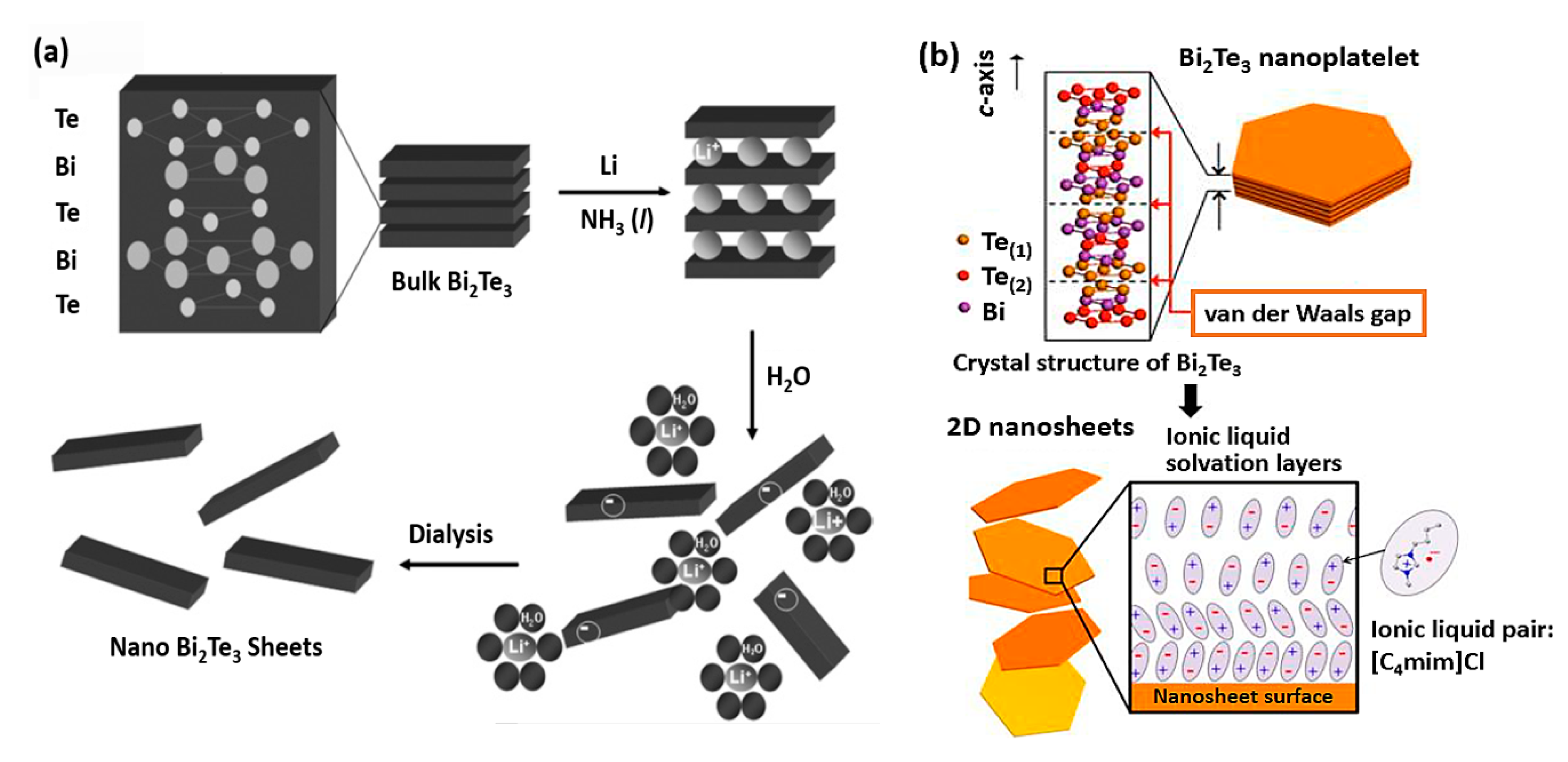
2.1. Liquid-Based Exfoliation Method

Ever since graphene was discovered, two-dimensional (2D) nanomaterials have gained tremendous interest in the research world due to their unique and extraordinary optical, electronic, thermal, and mechanical characteristics compared to their bulk counterparts [30,31]. In the nanostructure engineering of thermoelectric materials, the commonly used strategy to improve thermoelectric performance is to simultaneously reduce the thermal conductivity and enhance the electrical conductivity [10]. It has been demonstrated that lattice scattering of the phonons in nanoscaled layered thermoelectric materials would be able to effectively reduce the material’s thermal conductivity as the formation of nanostructures brings about lots of boundaries which act as effective phonon scattering centers [32]. Meanwhile, the charge carrier mobility on the 2D thin layers with higher crystallinity is greatly enhanced compared to the bulk material [33]. Thus, the performance of bulk thermoelectric materials has been improved with 2D nanostructures [34].
Currently, several methods for production of 2D metal chalcogenides have been developed, including the bottom-up synthesis by vapor-phase deposition [27,35,36], solvothermal method [37], and top-down approach by micromechanical cleavage [38]. However, those methods always suffer from harsh conditions such as high vacuum, high temperature, and/or slow throughput. The liquid exfoliation method is regarded as a highly scalable and achievable solution-based method for producing highly crystalline 2D nanomaterials with good yields in mild conditions [39,40,41]. The method utilizes high shearing or ultrasonication on crystal layers formed in their respective stabilizing liquids (such as surfactants, polymer solutions, ionic liquids, etc.) to produce 2D nanosheets. Net exfoliation energy is decreased by interactions of the molecules at the nanosheet–liquid interface, preventing the nanosheets from aggregating. The obtained dispersions are stable, and the nanosheets can be synthesized at a concentration of more than 1 g L−1. The liquid exfoliation method has been used in the synthesis of various 2D materials, including transition metal dichalcogenides, graphene, boron nitride, transition metal oxides, phosphorene, MXenes, and so on [39].
For Bi2Te3, each crystal layer is made up of approximately 1-nm thick quintuple sheets where the five atoms is covalently bonded in the order of Te1–Bi–Te2–Bi–Te1. The bulk material is then made up of weakly interacting stacked quintuple nanosheets [42]. Given the weak van der Waals forces of interaction between the layers, the 2D nanostructures can thus be formed by intercalation chemistry with exfoliation. In 2009, Ding and coworkers reported the lithium intercalation and exfoliation of layered Bi2Te3 and Bi2Se3 (Figure 2a) [43]. The intercalation of the lithium ions between the nanosheets is due to the reducing power of electrons solvated in liquid ammonia. The intercalated materials can be exfoliated in water with the assistance of ultrasonication to create colloidal suspensions. Dialysis can then be used to remove the lithium ions after exfoliation. The colloidal suspensions can be coated onto different substrates to form 2D flimsy oriented thin films. Very recently, Ju et al. prepared S-doped SnSe nanosheets by hydrothermal lithium intercalation and subsequent exfoliation from bulk ingots [44]. The substitution of S atoms is beneficial for the phonon scattering from many atomic disorders and nanosized boundaries, leading to effective reduction in thermal conductivity. Furthermore, through solution-phase chemical transformation of the obtained SnSe1−xSx nanosheets using tartaric acid, which can partially dissolve Sn2+ ions, a highly porous structure can be generated with further decreased thermal conductivity due to the scattering effect caused by the nanoscale porous boundaries. The fabricated porous SnSe1−xSx nanosheets exhibit a low thermal conductivity of 0.4 W m−1K−1 and a maximal ZT value of 0.12 at 310 K, which is significantly higher than that of pristine SnSe.
Room-temperature ionic liquids are superior exfoliants as they possess attractive physical and chemical properties including tunable viscosity, low vapor pressure, high ionic conductivity, and high thermal stability, and they can potentially be recycled. In 2015, Turner and coworkers studied the liquid exfoliation of Bi2Te3 nanoplatelets in an ionic liquid (1-butyl-3-methylimidazolium chloride, [C4mim]Cl) solvent (Figure 2b) [45]. Both experiments and molecular dynamics simulations demonstrated that the [C4mim]+ cation is the dominant factor for the interlayer sliding and separation of Bi2Te3 layers. Bi2Te3 nanoplatelets in [C4mim]Cl were synthesized at 0.05 wt % through 1-h tip sonication at a temperature of 80−150 °C and a power of 225–600 W. After sonication, as-synthesized nanoplatelets with a thickness of 1 to 2 μm were exfoliated to 15 ± 8 nm nanosheets. Later, the same group examined different exfoliation solvents and dispersion of Bi2Te3 from eight imidazolium-based ionic liquids at temperatures between 350 to 550 K [46].
Electrochemical exfoliation methods are gaining great research interest as the procedure is simple and the synthetic conditions are mild and easily controllable with high efficiencies. They can be applied to layered bulk materials in a liquid electrolyte to induce structural expansion. Promising methods for large-scale exfoliation of 2D materials include cathodic exfoliation or anodic oxidation–cationic intercalation. These layered bulk materials contain robust in-plane covalent bonds, but out-of-plane bonds that are held by weak van der Waals forces allow easy exfoliation into thin 2D nanosheets by charged ions [47]. In 2016, Ambrosi et al. reported the exfoliation of layered Bi2Te3 via electrochemistry (Figure 3) [48]. In this method, small flakes from the synthesized crystals were electrically connected to one electrode through a copper tape with a counter electrode made of Pt foil. Exfoliation was simply carried out by alternating the voltages from the anode (+10 V) and cathode (−10 V) to a solution of 0.5 M Na2SO4 electrolyte containing the crystals.

2.2. Hydrothermal or Solvothermal Method

Hydrothermal synthesis involves the growth of crystals from submicron to nanometer scale by chemical reaction in an aqueous solution at elevated temperature and high pressure. This method has been widely used since the 1960s for the synthesis of functional nanomaterials with different specific shapes and sizes [12,49]. Precise control over the internal reaction conditions, including pressure, time, pH value, concentration, and organic additives or templates, and external reaction environment, such as microwave or conventional heating, is necessary for the successful synthesis of the inorganic semiconducting nanostructures. By varying these two internal and external conditions, different hydrothermal synthesis methods have been developed [50].
To have greater control over the size, shape, reactivity, and phase of the product, the solvothermal method can be employed by using more different organic solvents rather than water. The solvent properties such as viscosity and polarity can influence the transport behavior and solubility of the reagents in the liquid medium. Compared to hydrothermal synthesis, solvothermal synthesis showed a higher tolerance as it could be carried out in a solvent with a higher reaction temperature [12].
Since the properties of inorganic semiconductors largely depend on their size, shape, and crystallinity, the highly controllable hydrothermal/solvothermal method has exhibited extraordinary advantages in the synthesis of inorganic semiconducting nanostructures due to simple manipulation, high yield, low energy consumption, good crystallinity, homogeneity, and narrow size distribution. By using this method, a number of nanostructured metal chalcogenides (based on Bi2Te3, Cu2Se, and SnSe) with different morphologies (Figure 4), such as nanostrings [51], nanorods [52,53], nanowires [54], nanobelts [55], nanoplates [56,57,58,59,60,61,62,63], nanoflowers [56,64], and nanopowder [65], have been synthesized and evaluated for thermoelectric applications. Yang et al. reported highly crystalline β-phase Cu2Se nanosheets prepared through heating the mixture of CuO, SeO2, NaOH, and polyvinylpyrrolidone (PVP) in ethylene glycol at 230 °C for 24 h. After sparking plasma sintering, the obtained Cu2Se pellets exhibit an ultralow thermal conductivity (0.2 W m−1K−1) due to strong phonon scattering by high-density small-angle grain boundaries in the nanostructured material, which leads to a considerably high ZT of 1.82 at 850 K. Zhao et al. reported the preparation of nanostructured Bi2Te3 with different morphologies (such as nanotubes, needle-shaped nanowires, nanoflakes, and flower-like clusters) by a facile hydrothermal treatment using sodium dodecyl benzene sulfonate (SDBS) and PVP as surfactants [43]. Results show that the formation of nanostructures can be readily controlled and tuned by the use of different surfactants and varying the reaction temperatures. Another significant advantage of the hydrothermal/solvothermal method is its great convenience for incorporation of different levels of element doping via addition of the corresponding precursors in the reaction mixture. Wu et al. synthesized Ce-, Y-, and Sm-doped Bi2T3 nanopowders via hydrothermal treatment [51]. Doping with these rare earth elements can effectively decrease the thermal conductivity, especially for the Ce-doped material, which exhibits a ZT value up to 1.29 at 373 K. The thermoelectric properties of these nanostructured metal chalcogenides prepared by hydrothermal/solvothermal method and other solution-based approaches are summarized in Table 1.

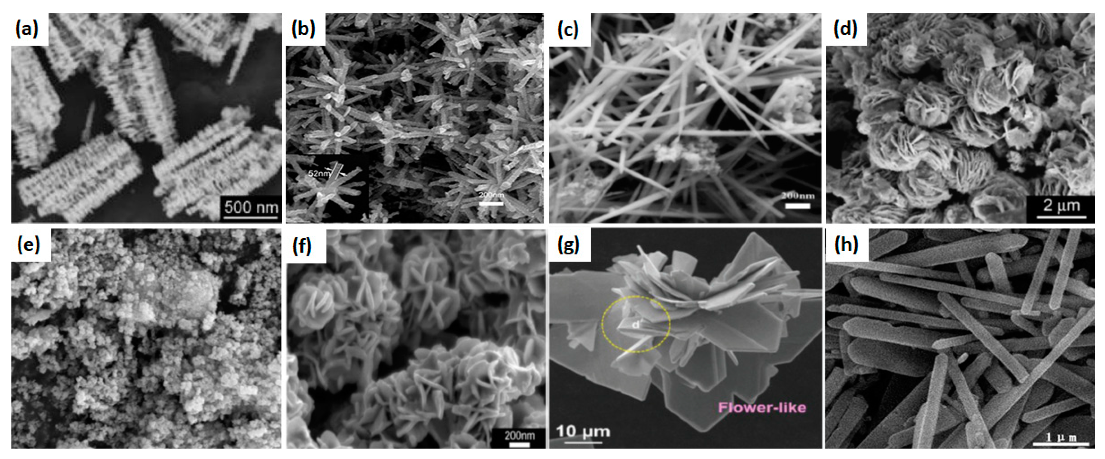
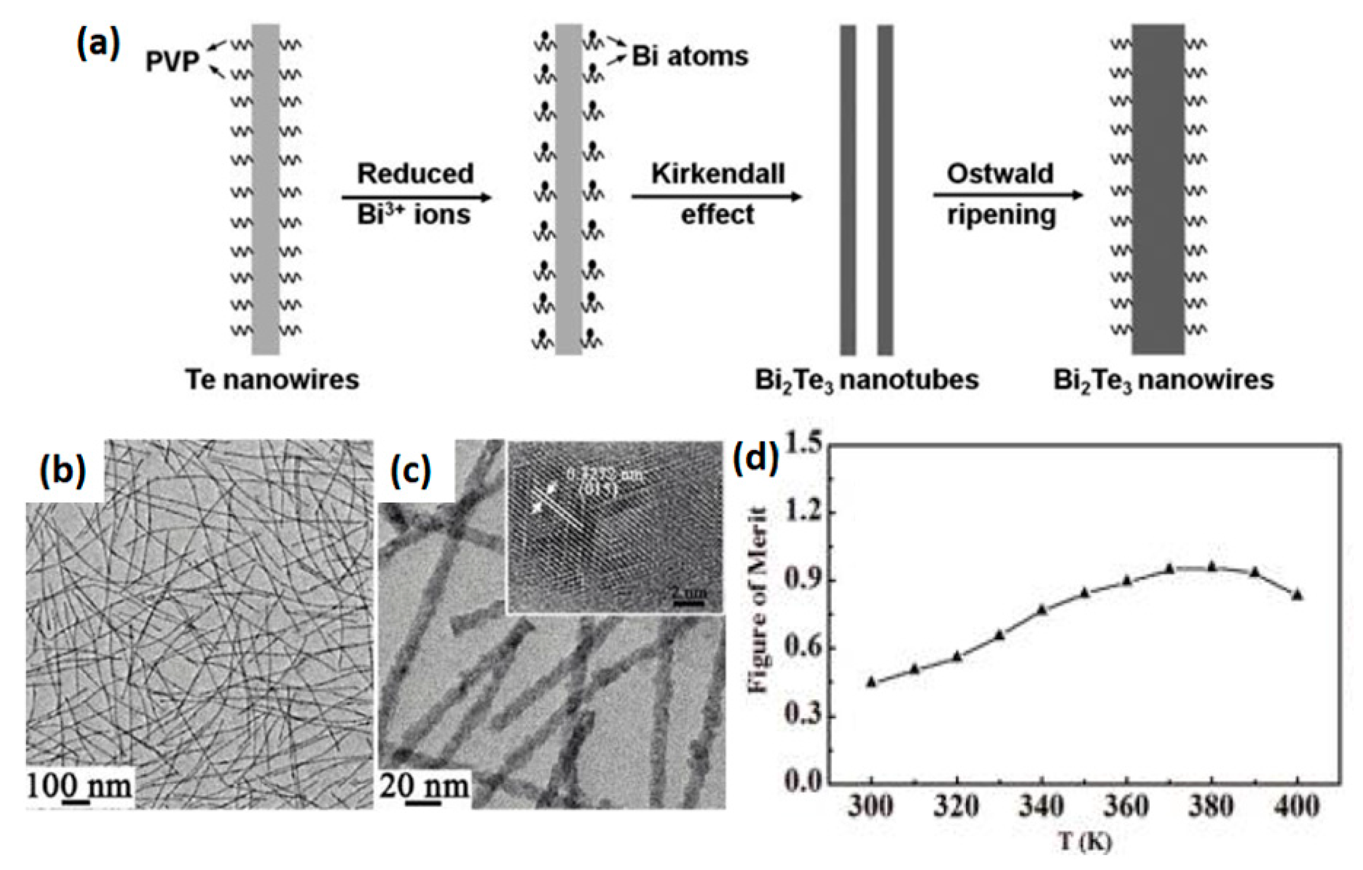
2.3. Template-Assisted Solution-Phase Synthesis

For the past 20 years, template-directed synthesis has been a commonly used method for the fabrication of 1D nanostructures [74,75,76]. In 2011, Wang et al. first reported a wet chemistry method for the controlled formation of ultrathin Te nanowires (with a diameter of several nanometers) using PVP as surfactant, which were subsequently employed as sacrificial templates to synthesize highly uniform Bi2Te3 nanowires with diameter of 15–17 nm and length of tens of micrometers in triethylene glycol solution upon addition of Bi3+ ions and hydrazine under heating (200 °C) at atmospheric pressure [68]. The synthesis of Bi2Te3 nanowires was said to have involved the Kirkendall effect and Ostwald ripening (Figure 5a), as evidenced by experimental observations. Using a similar method, Zhang et al. later carried out a simple and efficient synthesis of n-type ultrathin Bi2Te3 nanowires with an average diameter of 8 nm in ethylene glycol solution with high yield up to 93% (Figure 5b–d) [69]. The prepared Bi2Te3 nanowires were compressed to bulk pellets by spark plasma sintering and exhibited a high ZT value of 0.96 at 380 K, which was attributed to the notable decrease in thermal conductivity due to the increased phonon scattering at the boundaries of the nanowires. Very recently, Finefrock et al. also developed a large-scale one-pot solution-phase synthesis of ultrathin PbTe and Bi2Te3 nanowires (<15 nm) using Te nanowires as templates with high yield (>80%) at lower temperature (120 °C) in ethylene glycol solution [77]. This facile and scalable solution-phase approach is a promising and reliable route for manufacturing uniform ultrathin metal chalcogenide nanowires for thermoelectric applications.

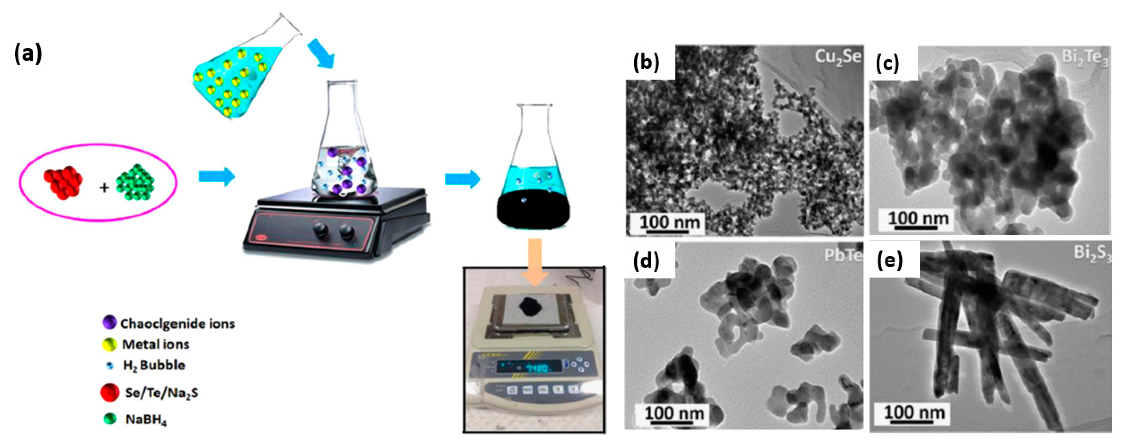
2.4. Chemical Reduction–Precipitation Method

Very recently, Han and coworkers developed a general ambient aqueous method for large-scale production of different nanostructured metal chalcogenides (y via a reduction–precipitation process without using any surfactants [70]. In a typical experiment (Figure 6a), NaBH4 was used to reduce Se powder in an aqueous solution. Copper precursor in distilled water was then added into the reaction mixture to yield black precipitates due to the poor solubility of copper selenide. The whole synthesis process took only one hour with high yield over 90%. Figure 6b–e presents the TEM images of different metal chalcogenide nanostructures prepared by this method. Most metal chalcogenides exhibit spherical morphology with a narrow size distribution of 10–20 nm. The possibility of such uniformed nanosized particles without addition of surfactants is due to the extremely low solubility of the nanoparticles, which gives rise to homogeneous precipitation from the aqueous solution. The thermoelectric properties of these nanoparticles were investigated after sintering into pellets using the spark plasma sintering technique. Pronounced enhancement in the ZT value was observed with some metal chalcogenide nanostructures (ZTmax = 0.38 at 300 °C for SnSe; ZTmax = 0.27 at 230 °C for Bi2Se3) due to the effectively reduced thermal conductivity. Li and coworkers also reported a wet coprecipitation method for large-scale synthesis of Cu2Se nanoparticles, which exhibited an outstanding ZT value (up to 1.35 at 850 K) after hot press sintering [71]. Pejjai et al. developed a similar eco-friendly reduction–precipitation approach to prepare SnSe nanoparticles in a short reaction time of 10 min [78].

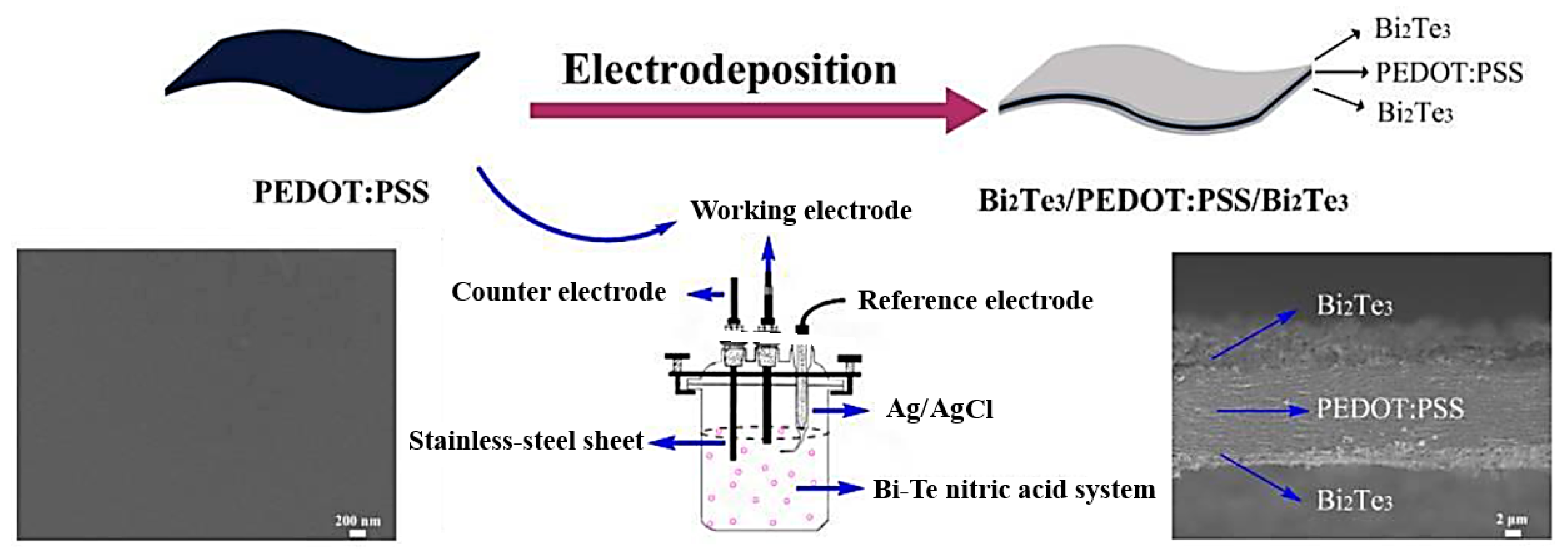
2.5. Electrodeposition Method

The electrodeposition method has been considered as an effective process to fabricate metallic coatings on a substrate surface through a cathodic reduction reaction in either an aqueous or an organic solution containing the metal ions to be electrodeposited [32,79,80,81]. The substrate material (such as indium–tin oxide (ITO), silicon, copper, porous anodic alumina (PAA) membranes, etc.) is used as the cathode to attract positively charged metallic ions and reduce them to their metallic form as a coating on the surface. The experimental parameters, such as electrolytes, reagent concentrations, nature of electrodes, temperature, and applied electrical conditions, could have effects on the properties of the electrodeposited films. This electrochemical synthesis process is scalable, simple, rapid, and cost-effective and it gives great control of the thickness, crystallinity, composition, and morphology. Electrodeposition has been extensively applied to fabricate various metal chalcogenide thermoelectric materials (Figure 7), such as Bi2Te3 films [59,72,73,82,83,84,85,86,87,88,89], Bi2Te3 nanowire arrays [90,91,92,93], Bi2Te3 nanotube arrays [94], Cu2Te films [95,96], Cu2Te nanowires [97], SnSe films [98,99,100,101], and so on.
In an early study, Miyazaki et al. prepared both n-type and p-type Bi2Te3 films via electrodeposition from a nitric acid bath containing Bi3+ and HTeO2+ via tuning the applied potential [86]. Most of the successive work on electrodeposition of Bi2Te3 films was carried out in a similar acidic aqueous solution of 1 M HNO3, which can only dissolve about 20 mM Te species. The low concentration of metal ions and mass transport in the solution resulted in inhomogeneous composition, a limited growth rate, and low film thickness (<10 µm). Nguyen and coworkers investigated organic electrolyte ethylene glycol, which provided advantages such as high metal ion solubility and wide electrochemical window, for electrodeposition of thick Bi2Te3 films (up to 67 µm) with uniform composition [85]. Naylor et al. reported that using sodium lignosulfonate surfactant in the reaction can lead to reduction in Bi2Te3 crystallite size to 20.8 nm and improvement of film alignment onto the preferred (110) orientation [87]. Recently, Yang et al. prepared electrodeposited films of a Cu–Se binary compound from solutions containing CuSO4, H2SeO3, and H2SO4. The copper contents and morphology of the films can be tuned via shifting the depositing potential [95]. The highest power factor for electrodeposited copper selenide film was 0.13 μW m−1 K−2 with a Seebeck coefficient of 56.0 µV K−1. A thin film thermoelectric power generator device containing 242 pairs of n-type Bi2Te3 and p-type Sb2Te3 thin-film legs on the bottom substrate was fabricated using the electrodeposition process [102].
Apart from the traditional substrates for electrodeposition, Jiang et al. recently reported using a free-standing poly(3,4-ethylenedioxythiophene):poly(styrenesulfonate) (PEDOT:PSS) film as the working electrode for electrodeposition of Bi2Te3 films for preparation of a sandwich-structured Bi2Te3/PEDOT:PSS/Bi2Te3 composite film (Figure 8) [103]. The as-prepared hybrid films exhibit a high electrical conductivity of 403.5 S cm−1 and a Seebeck coefficient of 15.3 µV K−1 with a favorable low thermal conductivity of 0.169–0.179 W m−1 K−1.
In addition to films, electrochemical deposition method can also be applied to produce nanowire or nanotube arrays using a hard-template-assisted method. Chen and coworkers prepared potentiostatically electrodeposited Bi2Te3 nanowire arrays embedded in an ordered porous anodic alumina membrane (AAM) template. Compared to the normal direct-current electrochemical deposition, the pulsed electrodeposition with a pulse delay time for the recovery of the ion concentration always leads to a crystalline structure with high orientation and good uniformity [104]. Li and coworkers fabricated highly oriented single-crystalline Bi2Te3 nanowire arrays by pulsed electrochemical deposition with an alternate pulse time of 3 ms and a delay time of 10 ms into the pores of the AAM template [91]. Lee et al. reported the tunable crystalline structure of the electrodeposited Bi2Te3 nanowires (with a Seebeck coefficient value of 12–33 μV K−1) by varying the delay times [92].

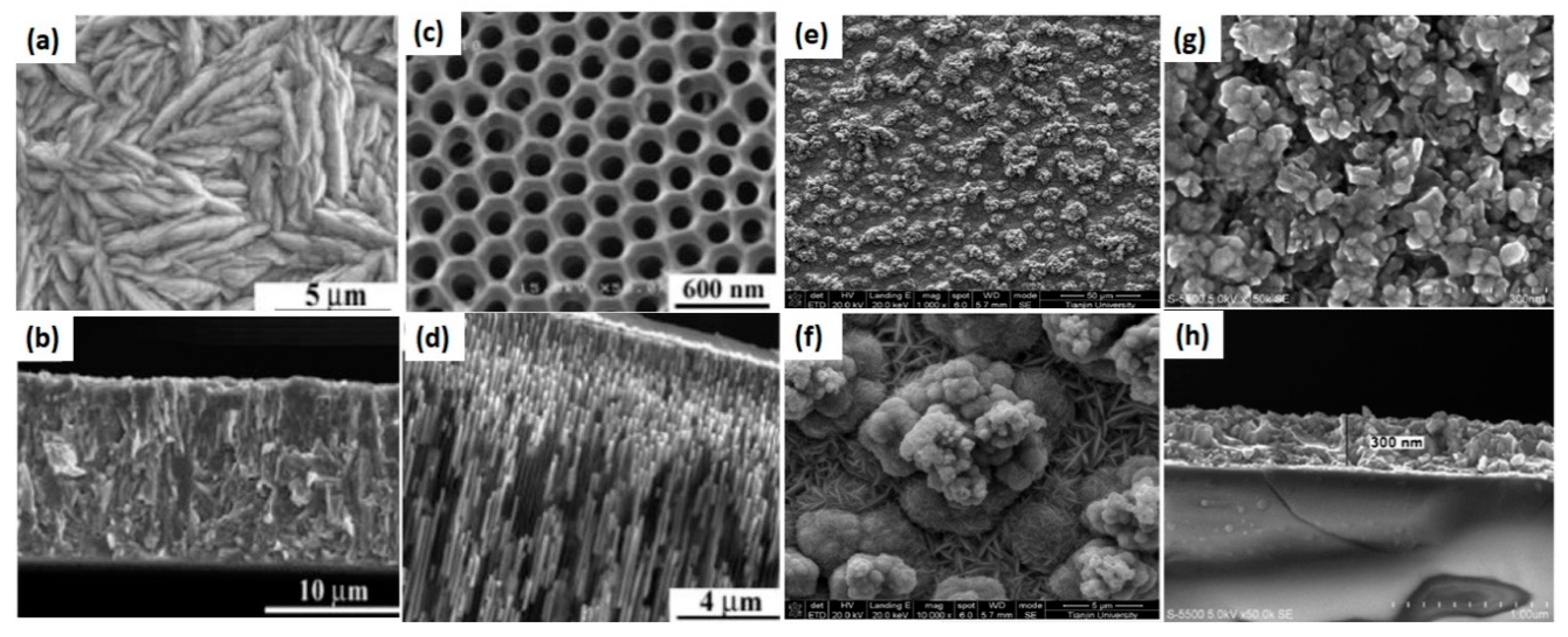
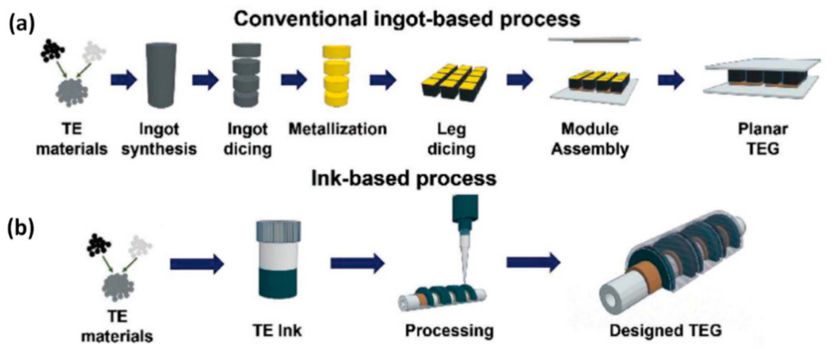
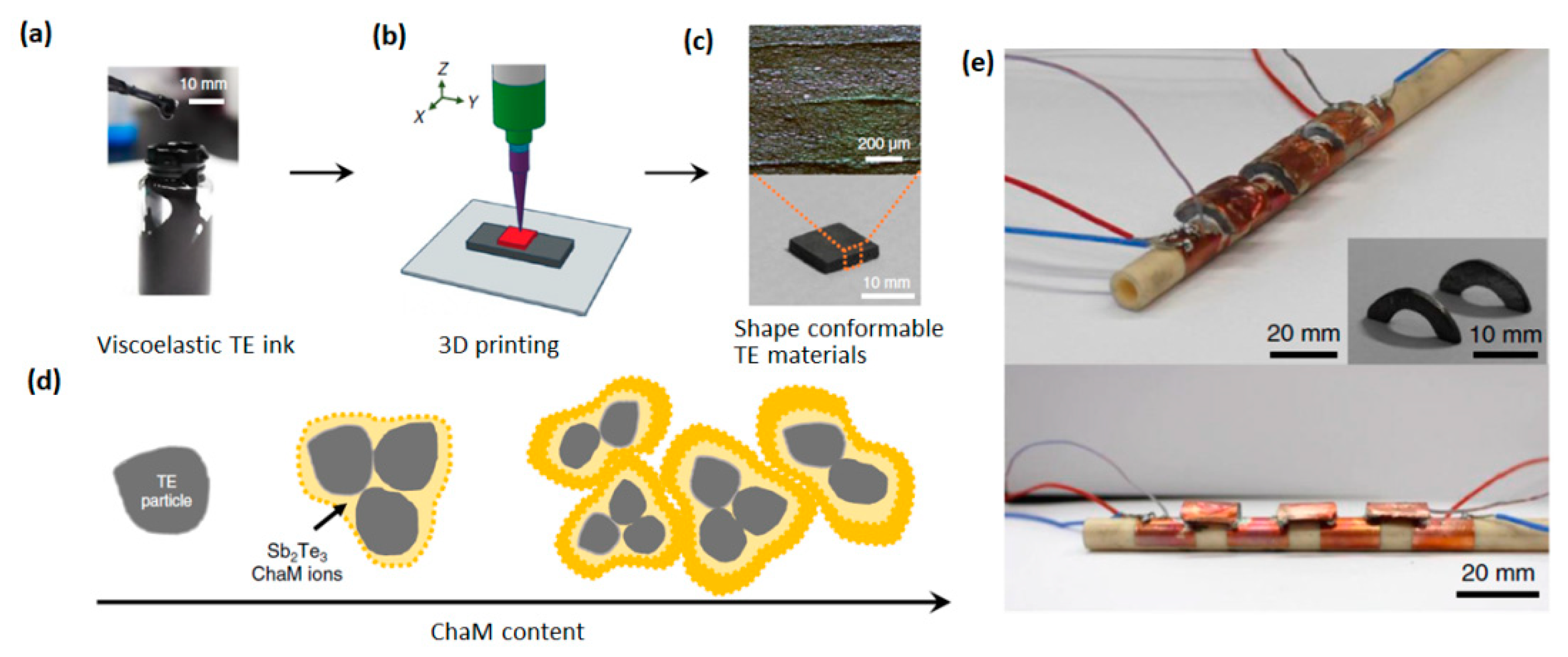
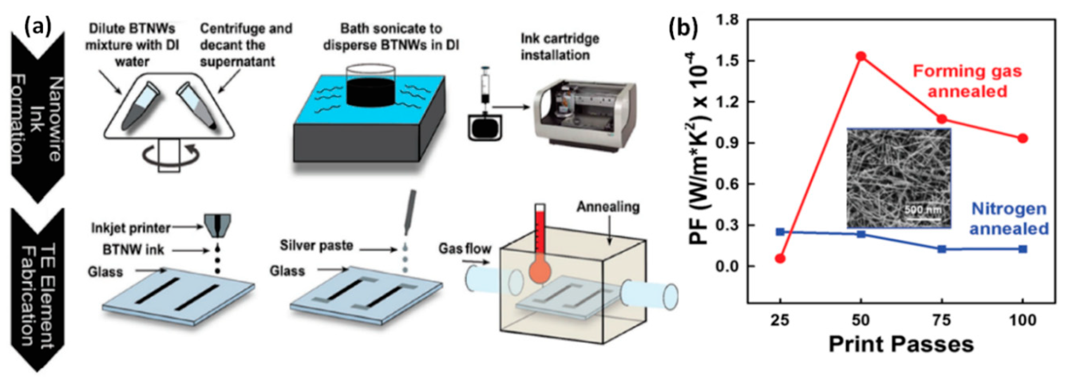
3. Ink-Based Processing Method for Thermoelectric Device Fabrication

The ink-based processing method is highly favorable as a cheaper method, including for large-scale device production. This method allows for easy assembly of thermoelectric device components, especially in the shaping and scaling of the thermoelectric legs. Ink-based processing can effectively reduce energy consumption for device fabrication and provide a high degree of design ability for thermoelectric generators (TEGs) [105].
Generally, thermoelectric inks are prepared from conductive polymers [106,107,108,109,110], hybrids of conductive polymers with inorganic or carbon nanofillers [111,112,113,114,115,116], and inorganic thermoelectric materials [117,118,119,120,121,122,123,124,125]. Currently, most thermoelectric devices are developed from inorganic materials due to their intrinsically higher power factors and ZT values compared to conductive polymers and organic–inorganic hybrid thermoelectric materials. The conventional route for fabrication of thermoelectric devices with inorganic materials involves multiple costly and time-consuming steps such as ingot synthesis, dicing, electroplating, assembling, cleaning, and soldering (Figure 9a). Moreover, the shapes of thermoelectric materials generated by the conventional method are mainly cuboids, giving rise to exclusively planar TEG geometries, and thus narrowing the application scope of thermoelectric power generation technology [105]. In comparison, the ink-based process exhibits great simplicity for patterning and shaping of thermoelectric materials into 2D films or even 3D bulk forms by drop-casting, spin-coating, spray-coating, inkjet-printing, screen-printing, dispenser-printing, and 3D-printing processes (Figure 9b) [126]. Table 2 summarizes the thermoelectric properties of various ink-processed metal chalcogenides and output power density of the derived TEG devices.
For thermoelectric inks of inorganic materials, several parameters such as concentration, dispersibility, and rheological properties should be optimized to make them suitable for the subsequent coating or printing process. Organic and polymer binders are always necessary to provide certain viscoelastic properties to the inks, which are eventually decomposed in the post-annealing step [118,119,120,121,124,125]. For example, Madan et al. prepared a slurry of Bi2Te3 particles and epoxy for dispenser printing of n-type Bi2Te3 thermoelectric generators [131]. Kim et al. developed a composite paste consisting of Bi and Te powders, organic binder, glass powder, and solvent by a ball-milling process [124], which can be used for fabrication of a flexible glass fabric-based TEG via the screen-printing method [118].
One problem with the addition of organic binders is that undesirable binder residues are at times trapped between the inorganic grains after the post-sintering stage, leading to compromised electrical properties and ZT values of the final thermoelectric products. In recent reports, inorganic chalcogenidometallate (ChaM) ions were observed to act as surface ligands for nano- and microscale particles, stabilizing these particles in the solution through electrostatic interactions [132]. In 2018, Kim and coworkers reported the extrusion-based 3D-printing of shape-conformable TE materials via full-inorganic Bi2Te3-based colloid inks using Sb2Te3 ChaM ions as inorganic binders (Figure 10) [123]. The ChaM inorganic ions can act as ligands to provide a charged surface for the Bi2Te3 particles, enhancing electrostatic interactions that contribute to the stability and viscoelasticity of the inks, and meanwhile facilitating 3D shape engineering and ensuring homogeneity of thermoelectric properties. These inks allowed for the fabrication of varied geometry thermoelectric materials that gave rise to high thermoelectric performances, as evidenced by their ZT values of 0.6 for n-type and 0.9 for p-type materials.
Recently, Chen et al. initially reported the inkjet printing of phase-pure, single-crystalline Bi2Te3 nanowires without adding any additives (Figure 11) [125]. The Bi2Te3 nanowires with an average diameter of 30 nm were synthesized by a chemical batch process, and then directly dispersed into deionized water by sonication to form the printable ink. Bi2Te3 films of different thickness (0.4–1.6 µm) were printed onto glass substrates and then subjected to post-annealing to improve the thermoelectric performance. The printed networks exhibited a Seebeck coefficient up to 140 μV K−1, which is comparable to that of Bi2Te3 nanowires that are hot-pressed into pellet form. High power factor (163 μW m−1 K−2) and thermoelectric efficiency (ZT ≈ 0.26) at room temperature are achieved with these printed films, which are promising for the scalable roll-to-roll manufacturing of printed thin-film thermoelectric devices.
In 2017, Lin et al. first reported a truly soluble thermoelectric ink, prepared at room temperature by dissolving Cu2Se powder in a mixed solvent of ethylenediamine and ethanedithiol, which can be directly coated onto various substrates via a low-cost and scalable spin-coating process (Figure 12) [117]. Owing to the high structural perfection, the Cu2Se thin film derived from the truly soluble ink material exhibits a considerably outstanding power factor of 0.62 mW m−1K−2 at 684 K on a rigid Al2O3 substrate and 0.46 mW m−1K−2 at 664 K on flexible polyimide film, which is greater than the values obtained from other solution-processed Cu2Se thin films (<0.1 mW m−1K−2) and amongst the highest values reported for flexible thermoelectric films (≈0.5 mW m−1K−2). In addition, the prepared thin film shows excellent stability after 1000 bending cycles, showing great promise for integration into various flexible electronics.

4. Conclusions and Outlook

The past few decades have witnessed a considerable growth in the synthesis and utilization of metal chalcogenide-based materials in different kinds of energy storage and conversion systems. The reliable and outstanding performance of these metal chalcogenides makes them the prime candidates for thermoelectric applications. In fact, their thermoelectric modules with ZT of around 1 have been successfully commercialized [133]. Nevertheless, to be competitive with other power generation systems, TEG materials should have a ZT of 2–3 at least. Further enhancement of conversion efficiency with these metal chalcogenide materials is being investigated through chemical doping and nanostructure engineering. This review mainly focused on the industry-friendly solution-based synthesis of nanoscaled or thin-film metal chalcogenides with controllable size, composition, morphology, and structure and their promising application as thermoelectric materials. The commonly used strategies can be categorized into the ‘top-down’ liquid exfoliation method and ‘bottom-up’ methods, including the hydrothermal/solvothermal process, template-assisted solution phase synthesis, chemical reduction–precipitation method, and electrodeposition method. In consideration of yield, production rate, crystallinity, and thermoelectric performance of the derived metal chalcogenide materials, the hydrothermal/solvothermal synthesis and wet chemical synthesis are most appropriate for practical large-scale production of these materials. The ink-based processing, together with various printing and coating methods, although still in the developing stage, is promising for cost-effective manufacturing of thin-film flexible thermoelectric devices.

Funding

This research was funded by A*STAR, SERC, and the Thermoelectric Materials Programme. Grant numbers: 1527200020 and 1527200021.

Acknowledgments

This work is also supported by the National University of Singapore, Department of Building.

Conflicts of Interest

The authors declare no conflict of interest.

References

  1. Minnich, A.J.; Dresselhaus, M.S.; Ren, Z.F.; Chen, G. Bulk nanostructured thermoelectric materials: Current research and future prospects. Energy Environ. Sci. 2009, 2, 466–479. [Google Scholar] [CrossRef]
  2. Snyder, G.J.; Toberer, E.S. Complex thermoelectric materials. Nat. Mater. 2008, 7, 105–114. [Google Scholar] [CrossRef] [PubMed]
  3. Dresselhaus, M.S.; Chen, G.; Tang, M.Y.; Yang, R.G.; Lee, H.; Wang, D.Z.; Ren, Z.F.; Fleurial, J.P.; Gogna, P. New directions for low-dimensional thermoelectric materials. Adv. Mater. 2007, 19, 1043–1053. [Google Scholar] [CrossRef]
  4. Zhang, X.; Zhao, L.-D. Thermoelectric materials: Energy conversion between heat and electricity. J. Mater. 2015, 1, 92–105. [Google Scholar] [CrossRef] [Green Version]
  5. Finefrock, S.W.; Yang, H.R.; Fang, H.Y.; Wu, Y. Thermoelectric Properties of Solution Synthesized Nanostructured Materials. In Annual Review of Chemical and Biomolecular Engineering; Prausnitz, J.M., Ed.; Annual Reviews: Palo Alto, CA, USA, 2015; Volume 6, pp. 247–266. [Google Scholar]
  6. Han, C.; Sun, Q.; Li, Z.; Dou, S.X. Thermoelectric enhancement of different kinds of metal chalcogenides. Adv. Energy Mater. 2016, 6, 1600498. [Google Scholar] [CrossRef]
  7. Chen, M.M.; Xue, H.G.; Guo, S.P. Multinary metal chalcogenides with tetrahedral structures for second-order nonlinear optical, photocatalytic, and photovoltaic applications. Coord. Chem. Rev. 2018, 368, 115–133. [Google Scholar] [CrossRef]
  8. Deng, Z.N.; Jiang, H.; Li, C.Z. 2D Metal Chalcogenides Incorporated into Carbon and their Assembly for Energy Storage Applications. Small 2018, 14, 9. [Google Scholar] [CrossRef]
  9. Guo, Z.N.; Sun, F.; Yuan, W.X. Chemical Intercalations in Layered Transition Metal Chalcogenides: Syntheses, Structures, and Related Properties. Cryst. Growth Des. 2017, 17, 2238–2253. [Google Scholar] [CrossRef]
  10. Jung, Y.; Zhou, Y.; Cha, J.J. Intercalation in two-dimensional transition metal chalcogenides. Inorg. Chem. Front. 2016, 3, 452–463. [Google Scholar] [CrossRef]
  11. Zhang, Y.; Zhou, Q.; Zhu, J.X.; Yan, Q.Y.; Dou, S.X.; Sun, W.P. Nanostructured Metal Chalcogenides for Energy Storage and Electrocatalysis. Adv. Funct. Mater. 2017, 27, 34. [Google Scholar] [CrossRef]
  12. Gao, M.-R.; Xu, Y.-F.; Jiang, J.; Yu, S.-H. Nanostructured metal chalcogenides: Synthesis, modification, and applications in energy conversion and storage devices. Chem. Soc. Rev. 2013, 42, 2986–3017. [Google Scholar] [CrossRef]
  13. Theerthagiri, J.; Karuppasamy, K.; Durai, G.; Rana, A.S.; Arunachalam, P.; Sangeetha, K.; Kuppusami, P.; Kim, H.S. Recent Advances in Metal Chalcogenides (MX; X = S, Se) Nanostructures for Electrochemical Supercapacitor Applications: A Brief Review. Nanomaterials 2018, 8, 256. [Google Scholar] [CrossRef]
  14. Xia, C.X.; Li, J.B. Recent advances in optoelectronic properties and applications of two-dimensional metal chalcogenides. J. Semicond. 2016, 37, 9. [Google Scholar] [CrossRef]
  15. Nie, L.N.; Zhang, Q.C. Recent progress in crystalline metal chalcogenides as efficient photocatalysts for organic pollutant degradation. Inorg. Chem. Front. 2017, 4, 1953–1962. [Google Scholar] [CrossRef]
  16. Gao, M.R.; Jiang, J.; Yu, S.H. Solution-based synthesis and design of late transition metal chalcogenide materials for oxygen reduction reaction (ORR). Small 2012, 8, 13–27. [Google Scholar] [CrossRef]
  17. Lhuillier, E.; Pedetti, S.; Ithurria, S.; Nadal, B.; Heuclin, H.; Dubertret, B. Two-Dimensional Colloidal Metal Chalcogenides Semiconductors: Synthesis, Spectroscopy, and Applications. Acc. Chem. Res. 2015, 48, 22–30. [Google Scholar] [CrossRef]
  18. Vaidhyanathan, B.; Ganguli, M.; Rao, K. Fast solid state synthesis of metal vanadates and chalcogenides using microwave irradiation. Mater. Res. Bull. 1995, 30, 1173–1177. [Google Scholar] [CrossRef]
  19. Carmalt, C.; Morrison, D.; Parkin, I. Solid-state and solution phase metathetical synthesis of copper indium chalcogenides. J. Mater. Chem. 1998, 8, 2209–2211. [Google Scholar] [CrossRef]
  20. Shaw, G.A.; Morrison, D.E.; Parkin, I.P. Solid state synthesis of binary metal chalcogenides. J. Chem. Soc. Dalton Trans. 2001, 1872–1875. [Google Scholar] [CrossRef]
  21. Li, H.; Wu, J.; Yin, Z.; Zhang, H. Preparation and applications of mechanically exfoliated single-layer and multilayer MoS2 and WSe2 nanosheets. Acc. Chem. Res. 2014, 47, 1067–1075. [Google Scholar] [CrossRef]
  22. Desai, S.B.; Madhvapathy, S.R.; Amani, M.; Kiriya, D.; Hettick, M.; Tosun, M.; Zhou, Y.; Dubey, M.; Ager, J.W., III; Chrzan, D. Gold-Mediated Exfoliation of Ultralarge Optoelectronically-Perfect Monolayers. Adv. Mater. 2016, 28, 4053–4058. [Google Scholar] [CrossRef]
  23. Magda, G.Z.; Pető, J.; Dobrik, G.; Hwang, C.; Biró, L.P.; Tapasztó, L. Exfoliation of large-area transition metal chalcogenide single layers. Sci. Rep. 2015, 5, 14714. [Google Scholar] [CrossRef] [Green Version]
  24. Cao, H.; Venkatasubramanian, R.; Liu, C.; Pierce, J.; Yang, H.; Zahid Hasan, M.; Wu, Y.; Chen, Y.P. Topological insulator Bi2Te3 films synthesized by metal organic chemical vapor deposition. Appl. Phys. Lett. 2012, 101, 162104. [Google Scholar] [CrossRef]
  25. Lee, C.W.; Kim, G.H.; Kang, S.G.; Kang, M.A.; An, K.S.; Kim, H.; Lee, Y.K. Growth behavior of Bi2Te3 and Sb2Te3 thin films on graphene substrate grown by plasma-enhanced chemical vapor deposition. Phys. Status Solidi (RRL)–Rapid Res. Lett. 2017, 11, 1600369. [Google Scholar] [CrossRef]
  26. Yu, J.; Hu, X.; Li, H.; Zhou, X.; Zhai, T. Large-scale synthesis of 2D metal dichalcogenides. J. Mater. Chem. C 2018, 6, 4627–4640. [Google Scholar] [CrossRef]
  27. Guo, L.L.; Ivey, B.C.; Aglan, A.; Tang, C.L.; Song, J.H.; Turner, C.H.; Frazier, R.M.; Gupta, A.; Wang, H.T. Vapor Phase Growth of Bismuth Telluride Nanoplatelets on Flexible Polyimide Films. ECS Solid State Lett. 2013, 2, P19–P21. [Google Scholar] [CrossRef]
  28. Tung, Y.; Chiang, Y.; Chong, C.; Deng, Z.; Chen, Y.; Huang, J.; Cheng, C.-M.; Pi, T.-W.; Tsuei, K.-D.; Li, Z. Growth and characterization of molecular beam epitaxy-grown Bi2Te3− xSex topological insulator alloys. J. Appl. Phys. 2016, 119, 055303. [Google Scholar] [CrossRef]
  29. Zeng, Z.; Morgan, T.A.; Fan, D.; Li, C.; Hirono, Y.; Hu, X.; Zhao, Y.; Lee, J.S.; Wang, J.; Wang, Z.M. Molecular beam epitaxial growth of Bi2Te3 and Sb2Te3 topological insulators on GaAs (111) substrates: A potential route to fabricate topological insulator p-n junction. AIP Adv. 2013, 3, 072112. [Google Scholar] [CrossRef]
  30. Tan, C.L.; Cao, X.H.; Wu, X.J.; He, Q.Y.; Yang, J.; Zhang, X.; Chen, J.Z.; Zhao, W.; Han, S.K.; Nam, G.H.; et al. Recent Advances in Ultrathin Two-Dimensional Nanomaterials. Chem. Rev. 2017, 117, 6225–6331. [Google Scholar] [CrossRef]
  31. Liu, B.; Zhou, K. Recent progress on graphene-analogous 2D nanomaterials: Properties, modeling and applications. Prog. Mater Sci. 2019, 100, 99–169. [Google Scholar] [CrossRef]
  32. Zhao, Y.X.; Dyck, J.S.; Burda, C. Toward high-performance nanostructured thermoelectric materials: The progress of bottom-up solution chemistry approaches. J. Mater. Chem. 2011, 21, 17049–17058. [Google Scholar] [CrossRef]
  33. Velický, M.; Toth, P.S. From two-dimensional materials to their heterostructures: An electrochemist’s perspective. Appl. Mater. Today 2017, 8, 68–103. [Google Scholar] [CrossRef]
  34. Zhou, Y.; Zhao, L.D. Promising thermoelectric bulk materials with 2D structures. Adv. Mater. 2017, 29, 1702676. [Google Scholar] [CrossRef]
  35. Zhao, Y.; Hughes, R.W.; Su, Z.; Zhou, W.; Gregory, D.H. One-Step Synthesis of Bismuth Telluride Nanosheets of a Few Quintuple Layers in Thickness. Angew. Chem. Int. Ed. 2011, 50, 10397–10401. [Google Scholar] [CrossRef]
  36. Kong, D.S.; Dang, W.H.; Cha, J.J.; Li, H.; Meister, S.; Peng, H.L.; Liu, Z.F.; Cui, Y. Few-Layer Nanoplates of Bi2Se3 and Bi2Te3 with Highly Tunable Chemical Potential. Nano Lett. 2010, 10, 2245–2250. [Google Scholar] [CrossRef]
  37. Fei, F.; Wei, Z.; Wang, Q.; Lu, P.; Wang, S.; Qin, Y.; Pan, D.; Zhao, B.; Wang, X.; Sun, J. Solvothermal synthesis of lateral heterojunction Sb2Te3/Bi2Te3 nanoplates. Nano Lett. 2015, 15, 5905–5911. [Google Scholar] [CrossRef]
  38. Teweldebrhan, D.; Goyal, V.; Balandin, A.A. Exfoliation and characterization of bismuth telluride atomic quintuples and quasi-two-dimensional crystals. Nano Lett. 2010, 10, 1209–1218. [Google Scholar] [CrossRef]
  39. Backes, C.; Higgins, T.M.; Kelly, A.; Boland, C.; Harvey, A.; Hanlon, D.; Coleman, J.N. Guidelines for exfoliation, characterization and processing of layered materials produced by liquid exfoliation. Chem. Mater. 2016, 29, 243–255. [Google Scholar] [CrossRef]
  40. Xu, Y.Y.; Cao, H.Z.; Xue, Y.Q.; Li, B.; Cai, W.H. Liquid-Phase Exfoliation of Graphene: An Overview on Exfoliation Media, Techniques, and Challenges. Nanomaterials 2018, 8, 942. [Google Scholar] [CrossRef]
  41. Coleman, J.N.; Lotya, M.; O’Neill, A.; Bergin, S.D.; King, P.J.; Khan, U.; Young, K.; Gaucher, A.; De, S.; Smith, R.J. Two-dimensional nanosheets produced by liquid exfoliation of layered materials. Science 2011, 331, 568–571. [Google Scholar] [CrossRef]
  42. Hong, S.S.; Kundhikanjana, W.; Cha, J.J.; Lai, K.; Kong, D.; Meister, S.; Kelly, M.A.; Shen, Z.-X.; Cui, Y. Ultra-thin Topological Insulator Bi2Se3 Nanoribbons Exfoliated by Atomic Force Microscopy. Nano Lett. 2010, 10, 3118–3122. [Google Scholar] [CrossRef]
  43. Ding, Z.; Bux, S.K.; King, D.J.; Chang, F.L.; Chen, T.-H.; Huang, S.-C.; Kaner, R.B. Lithium intercalation and exfoliation of layered bismuth selenide and bismuth telluride. J. Mater. Chem. 2009, 19, 2588–2592. [Google Scholar] [CrossRef]
  44. Ju, H.; Kim, M.; Park, D.; Kim, J. A Strategy for Low Thermal Conductivity and Enhanced Thermoelectric Performance in SnSe: Porous SnSe1–x S x Nanosheets. Chem. Mater. 2017, 29, 3228–3236. [Google Scholar] [CrossRef]
  45. Ludwig, T.; Guo, L.; McCrary, P.; Zhang, Z.; Gordon, H.; Quan, H.; Stanton, M.; Frazier, R.M.; Rogers, R.D.; Wang, H.-T. Mechanism of bismuth telluride exfoliation in an ionic liquid solvent. Langmuir 2015, 31, 3644–3652. [Google Scholar] [CrossRef]
  46. Abedini, A.; Ludwig, T.; Zhang, Z.; Turner, C.H. Molecular Dynamics Simulation of Bismuth Telluride Exfoliation Mechanisms in Different Ionic Liquid Solvents. Langmuir 2016, 32, 9982–9992. [Google Scholar] [CrossRef]
  47. Yang, Y.C.; Hou, H.S.; Zou, G.Q.; Shi, W.; Shuai, H.L.; Li, J.Y.; Ji, X.B. Electrochemical exfoliation of graphene-like two-dimensional nanomaterials. Nanoscale 2019, 11, 16–33. [Google Scholar] [CrossRef]
  48. Ambrosi, A.; Sofer, Z.k.; Luxa, J.; Pumera, M. Exfoliation of layered topological insulators Bi2Se3 and Bi2Te3 via electrochemistry. ACS Nano 2016, 10, 11442–11448. [Google Scholar] [CrossRef]
  49. Byrappa, K.; Adschiri, T. Hydrothermal technology for nanotechnology. Prog. Cryst. Growth Charact. Mater. 2007, 53, 117–166. [Google Scholar] [CrossRef] [Green Version]
  50. Shi, W.; Song, S.; Zhang, H. Hydrothermal synthetic strategies of inorganic semiconducting nanostructures. Chem. Soc. Rev. 2013, 42, 5714–5743. [Google Scholar] [CrossRef]
  51. Mi, J.L.; Lock, N.; Sun, T.; Christensen, M.; Sondergaard, M.; Hald, P.; Hng, H.H.; Ma, J.; Iversen, B.B. Biomolecule-Assisted Hydrothermal Synthesis and Self-Assembly of Bi2Te3 Nanostring-Cluster Hierarchical Structure. ACS Nano 2010, 4, 2523–2530. [Google Scholar] [CrossRef]
  52. Kundu, S.; Yi, S.I.; Yu, C. Gram-scale solution-based synthesis of SnSe thermoelectric nanomaterials. Appl. Surf. Sci. 2018, 459, 376–384. [Google Scholar] [CrossRef]
  53. Song, S.Y.; Fu, J.P.; Li, X.Y.; Gao, W.; Zhang, H.J. Facile Synthesis and Thermoelectric Properties of Self-assembled Bi2Te3 One-Dimensional Nanorod Bundles. Chem. A Eur. J. 2013, 19, 2889–2894. [Google Scholar] [CrossRef]
  54. Zhao, Q.; Wang, Y.G. A facile two-step hydrothermal route for the synthesis of low-dimensional structured Bi2Te3 nanocrystals with various morphologies. J. Alloy. Compd. 2010, 497, 57–61. [Google Scholar] [CrossRef]
  55. Guo, J.; Jian, J.K.; Liu, J.; Cao, B.L.; Lei, R.B.; Zhang, Z.H.; Song, B.; Zhao, H.Z. Synthesis of SnSe nanobelts and the enhanced thermoelectric performance in its hot-pressed bulk composite. Nano Energy 2017, 38, 569–575. [Google Scholar] [CrossRef]
  56. Fu, J.P.; Song, S.Y.; Zhang, X.G.; Cao, F.; Zhou, L.; Li, X.Y.; Zhang, H.J. Bi2Te3 nanoplates and nanoflowers: Synthesized by hydrothermal process and their enhanced thermoelectric properties. CrystEngComm 2012, 14, 2159–2165. [Google Scholar] [CrossRef]
  57. Hong, M.; Chasapis, T.C.; Chen, Z.G.; Yang, L.; Kanatzidis, M.G.; Snyder, G.J.; Zou, J. n-Type Bi2Te3-xSex Nanoplates with Enhanced Thermoelectric Efficiency Driven by Wide-Frequency Phonon Scatterings and Synergistic Carrier Scatterings. ACS Nano 2016, 10, 4719–4727. [Google Scholar] [CrossRef]
  58. Li, C.C.; Kong, F.F.; Liu, C.C.; Liu, H.X.; Hu, Y.J.; Wang, T.Z.; Xu, J.K.; Jiang, F.X. Dual-functional aniline-assisted wet-chemical synthesis of bismuth telluride nanoplatelets and their thermoelectric performance. Nanotechnology 2017, 28, 9. [Google Scholar] [CrossRef]
  59. Shi, X.L.; Chen, Z.G.; Liu, W.D.; Yang, L.; Hong, M.; Moshwan, R.; Huang, L.Q.; Zou, J. Achieving high Figure of Merit in p-type polycrystalline Sn0.98Se via self-doping and anisotropy-strengthening. Energy Storage Mater. 2018, 10, 130–138. [Google Scholar] [CrossRef]
  60. Shi, X.L.; Zheng, K.; Liu, W.D.; Wang, Y.; Yang, Y.Z.; Chen, Z.G.; Zou, J. Realizing High Thermoelectric Performance in n-Type Highly Distorted Sb-Doped SnSe Microplates via Tuning High Electron Concentration and Inducing Intensive Crystal Defects. Adv. Energy Mater. 2018, 8, 12. [Google Scholar] [CrossRef]
  61. Wang, J.; Liu, B.; Miao, N.; Zhou, J.; Sun, Z. I-doped Cu2Se nanocrystals for high-performance thermoelectric applications. J. Alloy. Compd. 2019, 772, 366–370. [Google Scholar] [CrossRef]
  62. Wu, F.; Song, H.Z.; Jia, J.F.; Hu, X. Effects of Ce, Y, and Sm doping on the thermoelectric properties of Bi2Te3 alloy. Prog. Nat. Sci. Mater. Int. 2013, 23, 408–412. [Google Scholar] [CrossRef]
  63. Yang, L.; Chen, Z.G.; Han, G.; Hong, M.; Zou, J. Impacts of Cu deficiency on the thermoelectric properties of Cu2-XSe nanoplates. Acta Mater. 2016, 113, 140–146. [Google Scholar] [CrossRef]
  64. Zhang, Y.H.; Zhu, T.J.; Tu, J.P.; Zhao, X.B. Flower-like nanostructure and thermoelectric properties of hydrothermally synthesized La-containing Bi2Te3 based alloys. Mater. Chem. Phys. 2007, 103, 484–488. [Google Scholar] [CrossRef]
  65. Shi, W.; Wu, F.; Wang, K.; Yang, J.; Song, H.; Hu, X. Preparation and thermoelectric properties of yttrium-doped Bi2Te3 flower-like nanopowders. J. Electron. Mater. 2014, 43, 3162–3168. [Google Scholar] [CrossRef]
  66. Salavati-Niasari, M.; Bazarganipour, M.; Davar, F. Hydrothermal preparation and characterization of based-alloy Bi2Te3 nanostructure with different morphology. J. Alloy. Compd. 2010, 489, 530–534. [Google Scholar] [CrossRef]
  67. Tang, Y.Q.; Ge, Z.H.; Feng, J. Synthesis and Thermoelectric Properties of Copper Sulfides via Solution Phase Methods and Spark Plasma Sintering. Crystals 2017, 7, 141. [Google Scholar] [CrossRef]
  68. Wang, K.; Liang, H.-W.; Yao, W.-T.; Yu, S.-H. Templating synthesis of uniform Bi2Te3 nanowires with high aspect ratio in triethylene glycol (TEG) and their thermoelectric performance. J. Mater. Chem. 2011, 21, 15057–15062. [Google Scholar] [CrossRef]
  69. Zhang, G.Q.; Kirk, B.; Jauregui, L.A.; Yang, H.R.; Xu, X.F.; Chen, Y.P.; Wu, Y. Rational Synthesis of Ultrathin n-Type Bi2Te3 Nanowires with Enhanced Thermoelectric Properties. Nano Lett. 2012, 12, 56–60. [Google Scholar] [CrossRef]
  70. Han, C.; Li, Z.; Lu, G.Q.; Dou, S.X. Robust scalable synthesis of surfactant-free thermoelectric metal chalcogenide nanostructures. Nano Energy 2015, 15, 193–204. [Google Scholar] [CrossRef] [Green Version]
  71. Li, D.; Qin, X.Y.; Liu, Y.F.; Song, C.J.; Wang, L.; Zhang, J.; Xin, H.X.; Guo, G.L.; Zou, T.H.; Sun, G.L. Chemical synthesis of nanostructured Cu2Se with high thermoelectric performance. Rsc Adv. 2014, 4, 8638–8644. [Google Scholar] [CrossRef]
  72. Chen, C.-L.; Chen, Y.-Y.; Lin, S.-J.; Ho, J.C.; Lee, P.-C.; Chen, C.-D.; Harutyunyan, S.R. Fabrication and characterization of electrodeposited bismuth telluride films and nanowires. J. Phys. Chem. C 2010, 114, 3385–3389. [Google Scholar] [CrossRef]
  73. Manzano, C.V.; Abad, B.; Rojo, M.M.; Koh, Y.R.; Hodson, S.L.; Martinez, A.M.L.; Xu, X.F.; Shakouri, A.; Sands, T.D.; Borca-Tasciuc, T.; et al. Anisotropic Effects on the Thermoelectric Properties of Highly Oriented Electrodeposited Bi2Te3 Films. Sci. Rep. 2016, 6, 8. [Google Scholar] [CrossRef]
  74. Moon, G.D.; Ko, S.; Xia, Y.; Jeong, U. Chemical transformations in ultrathin chalcogenide nanowires. ACS Nano 2010, 4, 2307–2319. [Google Scholar] [CrossRef]
  75. Moon, G.D.; Ko, S.; Min, Y.; Zeng, J.; Xia, Y.; Jeong, U. Chemical transformations of nanostructured materials. Nano Today 2011, 6, 186–203. [Google Scholar] [CrossRef]
  76. Liang, H.W.; Liu, S.; Yu, S.H. Controlled synthesis of one-dimensional inorganic nanostructures using pre-existing one-dimensional nanostructures as templates. Adv. Mater. 2010, 22, 3925–3937. [Google Scholar] [CrossRef]
  77. Finefrock, S.W.; Fang, H.; Yang, H.; Darsono, H.; Wu, Y. Large-scale solution-phase production of Bi2Te3 and PbTe nanowires using Te nanowire templates. Nanoscale 2014, 6, 7872–7876. [Google Scholar] [CrossRef]
  78. Pejjai, B.; Reddy, V.R.M.; Seku, K.; Pallavolu, M.R.; Park, C. Eco-friendly synthesis of SnSe nanoparticles: Effect of reducing agents on the reactivity of a Se-precursor and phase formation of SnSe NPs. New J. Chem. 2018, 42, 4843–4853. [Google Scholar] [CrossRef]
  79. Gurrappa, I.; Binder, L. Electrodeposition of nanostructured coatings and their characterization—a review. Sci. Technol. Adv. Mater. 2008, 9, 043001. [Google Scholar] [CrossRef]
  80. Rostek, R.; Stein, N.; Boulanger, C. A review of electroplating for V-VI thermoelectric films: From synthesis to device integration. J. Mater. Res. 2015, 30, 2518–2543. [Google Scholar] [CrossRef]
  81. Bicelli, L.P.; Bozzini, B.; Mele, C.; D’Urzo, L. A review of nanostructural aspects of metal electrodeposition. Int. J. Electrochem. Sci 2008, 3, 356–408. [Google Scholar]
  82. Menke, E.; Li, Q.; Penner, R. Bismuth telluride (Bi2Te3) nanowires synthesized by cyclic electrodeposition/stripping coupled with step edge decoration. Nano Lett. 2004, 4, 2009–2014. [Google Scholar] [CrossRef]
  83. Wang, W.-L.; Wan, C.-C.; Wang, Y.-Y. Composition-dependent characterization and optimal control of electrodeposited Bi2Te3 films for thermoelectric application. Electrochim. Acta 2007, 52, 6502–6508. [Google Scholar] [CrossRef]
  84. Heo, P.; Hagiwara, K.; Ichino, R.; Okido, M. Electrodeposition and thermoelectric characterization of Bi2Te3. J. Electrochem. Soc. 2006, 153, C213–C217. [Google Scholar] [CrossRef]
  85. Nguyen, H.P.; Wu, M.X.; Su, J.L.; Vullers, R.J.M.; Vereecken, P.M.; Fransaer, J. Electrodeposition of bismuth telluride thermoelectric films from a nonaqueous electrolyte using ethylene glycol. Electrochim. Acta 2012, 68, 9–17. [Google Scholar] [CrossRef]
  86. Miyazaki, Y.; Kajitani, T. Preparation of Bi2Te3 films by electrodeposition. J. Cryst. Growth 2001, 229, 542–546. [Google Scholar] [CrossRef]
  87. Naylor, A.J.; Koukharenko, E.; Nandhakumar, I.S.; White, N.M. Surfactant-Mediated Electrodeposition of Bismuth Telluride Films and Its Effect on Microstructural Properties. Langmuir 2012, 28, 8296–8299. [Google Scholar] [CrossRef]
  88. Ma, Y.; Ahlberg, E.; Sun, Y.; Iversen, B.B.; Palmqvist, A.E. Thermoelectric properties of thin films of bismuth telluride electrochemically deposited on stainless steel substrates. Electrochim. Acta 2011, 56, 4216–4223. [Google Scholar] [CrossRef]
  89. Yoo, B.Y.; Huang, C.K.; Lim, J.R.; Herman, J.; Ryan, M.A.; Fleurial, J.P.; Myung, N.V. Electrochemically deposited thermoelectric n-type Bi2Te3 thin films. Electrochim. Acta 2005, 50, 4371–4377. [Google Scholar] [CrossRef]
  90. Prieto, A.L.; Sander, M.S.; Martín-González, M.S.; Gronsky, R.; Sands, T.; Stacy, A.M. Electrodeposition of ordered Bi2Te3 nanowire arrays. J. Am. Chem. Soc. 2001, 123, 7160–7161. [Google Scholar] [CrossRef]
  91. Li, L.; Yang, Y.; Huang, X.; Li, G.; Zhang, L. Pulsed electrodeposition of single-crystalline Bi2Te3 nanowire arrays. Nanotechnology 2006, 17, 1706. [Google Scholar] [CrossRef]
  92. Lee, J.; Farhangfar, S.; Lee, J.; Cagnon, L.; Scholz, R.; Gösele, U.; Nielsch, K. Tuning the crystallinity of thermoelectric Bi2Te3 nanowire arrays grown by pulsed electrodeposition. Nanotechnology 2008, 19, 365701. [Google Scholar] [CrossRef]
  93. Sander, M.; Prieto, A.; Gronsky, R.; Sands, T.; Stacy, A.M. Fabrication of High-Density, High Aspect Ratio, Large-Area Bismuth Telluride Nanowire Arrays by Electrodeposition into Porous Anodic Alumina Templates. Adv. Mater. 2002, 14, 665–667. [Google Scholar] [CrossRef]
  94. Li, X.-H.; Zhou, B.; Pu, L.; Zhu, J.-J. Electrodeposition of Bi2Te3 and Bi2Te3 derived alloy nanotube arrays. Cryst. Growth Des. 2008, 8, 771–775. [Google Scholar] [CrossRef]
  95. Yang, M.Q.; Shen, Z.W.; Liu, X.Q.; Wang, W. Electrodeposition and Thermoelectric Properties of Cu-Se Binary Compound Films. J. Electron. Mater. 2016, 45, 1974–1981. [Google Scholar] [CrossRef]
  96. Lippkow, D.; Strehblow, H.-H. Structural investigations of thin films of copper–selenide electrodeposited at elevated temperatures. Electrochim. Acta 1998, 43, 2131–2140. [Google Scholar] [CrossRef]
  97. Kaur, H.; Kaur, J.; Singh, L.; Singh, S. Electrochemical synthesis and characterization of Cu2Se nanowires. Superlattices Microstruct. 2013, 64, 294–302. [Google Scholar] [CrossRef]
  98. Ananthi, K.; Thilakavathy, K.; Muthukumarasamy, N.; Dhanapandian, S.; Murali, K. Properties of pulse plated SnSe films. J. Mater. Sci.: Mater. Electron. 2012, 23, 1338–1341. [Google Scholar] [CrossRef]
  99. Bicer, M.; Şişman, İ. Electrodeposition and growth mechanism of SnSe thin films. Appl. Surf. Sci. 2011, 257, 2944–2949. [Google Scholar] [CrossRef]
  100. Mathews, N. Electrodeposited tin selenide thin films for photovoltaic applications. Sol. Energy 2012, 86, 1010–1016. [Google Scholar] [CrossRef]
  101. Zainal, Z.; Ali, A.J.; Kassim, A.; Hussein, M.Z. Electrodeposition of tin selenide thin film semiconductor: Effect of the electrolytes concentration on the film properties. Sol. Energy Mater. Sol. Cells 2003, 79, 125–132. [Google Scholar] [CrossRef]
  102. Kim, M.-Y.; Oh, T.-S. Thermoelectric power generation characteristics of a thin-film device consisting of electrodeposited n-Bi2Te3 and p-Sb2Te3 thin-film legs. J. Electron. Mater. 2013, 42, 2752–2757. [Google Scholar] [CrossRef]
  103. Jiang, Q.; Liu, C.; Song, H.; Xu, J.; Mo, D.; Shi, H.; Wang, Z.; Jiang, F.; Lu, B.; Zhu, Z. Free-standing PEDOT: PSS film as electrode for the electrodeposition of bismuth telluride and its thermoelectric performance. Int. J. Electrochem. Sci 2014, 9, 7540–7551. [Google Scholar]
  104. Larson, C.; Farr, J. Recent advances in pulsed current electrodeposition: A brief review. Trans. IMF 2010, 88, 237–242. [Google Scholar] [CrossRef]
  105. Jo, S.; Choo, S.; Kim, F.; Heo, S.H.; Son, J.S. Ink Processing for Thermoelectric Materials and Power-Generating Devices. Adv. Mater. 2018, 1804930. [Google Scholar] [CrossRef]
  106. Zhang, Q.; Sun, Y.; Xu, W.; Zhu, D. Thermoelectric energy from flexible P3HT films doped with a ferric salt of triflimide anions. Energy Environ. Sci. 2012, 5, 9639–9644. [Google Scholar] [CrossRef]
  107. Hwang, S.; Potscavage, W.J.; Yang, Y.S.; Park, I.S.; Matsushima, T.; Adachi, C. Solution-processed organic thermoelectric materials exhibiting doping-concentration-dependent polarity. Phys. Chem. Chem. Phys. 2016, 18, 29199–29207. [Google Scholar] [CrossRef]
  108. Taggart, D.K.; Yang, Y.; Kung, S.-C.; McIntire, T.M.; Penner, R.M. Enhanced thermoelectric metrics in ultra-long electrodeposited PEDOT nanowires. Nano Lett. 2010, 11, 125–131. [Google Scholar] [CrossRef]
  109. Kim, G.-H.; Shao, L.; Zhang, K.; Pipe, K.P. Engineered doping of organic semiconductors for enhanced thermoelectric efficiency. Nat. Mater. 2013, 12, 719. [Google Scholar] [CrossRef]
  110. Aïch, R.B.; Blouin, N.; Bouchard, A.; Leclerc, M. Electrical and thermoelectric properties of poly (2, 7-carbazole) derivatives. Chem. Mater. 2009, 21, 751–757. [Google Scholar] [CrossRef]
  111. Jiang, F.; Xiong, J.; Zhou, W.; Liu, C.; Wang, L.; Zhao, F.; Liu, H.; Xu, J. Use of organic solvent-assisted exfoliated MoS 2 for optimizing the thermoelectric performance of flexible PEDOT: PSS thin films. J. Mater. Chem. A 2016, 4, 5265–5273. [Google Scholar] [CrossRef]
  112. Ju, H.; Kim, J. Chemically exfoliated SnSe nanosheets and their SnSe/poly(3,4-ethylenedioxythiophene): Poly(styrenesulfonate) composite films for polymer based thermoelectric applications. ACS Nano 2016, 10, 5730–5739. [Google Scholar] [CrossRef]
  113. Choi, J.; Lee, J.Y.; Lee, S.S.; Park, C.R.; Kim, H. High-Performance Thermoelectric Paper Based on Double Carrier-Filtering Processes at Nanowire Heterojunctions. Adv. Energy Mater. 2016, 6, 1502181. [Google Scholar] [CrossRef]
  114. Kato, K.; Hagino, H.; Miyazaki, K. Fabrication of bismuth telluride thermoelectric films containing conductive polymers using a printing method. J. Electron. Mater. 2013, 42, 1313–1318. [Google Scholar] [CrossRef]
  115. Toshima, N.; Imai, M.; Ichikawa, S. Organic–inorganic nanohybrids as novel thermoelectric materials: Hybrids of polyaniline and bismuth (III) telluride nanoparticles. J. Electron. Mater. 2011, 40, 898–902. [Google Scholar] [CrossRef]
  116. Zhang, B.; Sun, J.; Katz, H.; Fang, F.; Opila, R. Promising thermoelectric properties of commercial PEDOT: PSS materials and their Bi2Te3 powder composites. ACS Appl. Mater. Interfaces 2010, 2, 3170–3178. [Google Scholar] [CrossRef]
  117. Lin, Z.; Hollar, C.; Kang, J.S.; Yin, A.; Wang, Y.; Shiu, H.Y.; Huang, Y.; Hu, Y.; Zhang, Y.; Duan, X. A Solution Processable High-Performance Thermoelectric Copper Selenide Thin Film. Adv. Mater. 2017, 29, 1606662. [Google Scholar] [CrossRef]
  118. Kim, S.J.; We, J.H.; Cho, B.J. A wearable thermoelectric generator fabricated on a glass fabric. Energy Environ. Sci. 2014, 7, 1959–1965. [Google Scholar] [CrossRef]
  119. Choi, H.; Kim, S.J.; Kim, Y.; We, J.H.; Oh, M.-W.; Cho, B.J. Enhanced thermoelectric properties of screen-printed Bi0.5Sb1.5Te3 and Bi2Te2.7Se0.3 thick films using a post annealing process with mechanical pressure. J. Mater. Chem. C 2017, 5, 8559–8565. [Google Scholar] [CrossRef]
  120. Kim, S.J.; Choi, H.; Kim, Y.; We, J.H.; Shin, J.S.; Lee, H.E.; Oh, M.-W.; Lee, K.J.; Cho, B.J. Post ionized defect engineering of the screen-printed Bi2Te2.7Se0.3 thick film for high performance flexible thermoelectric generator. Nano Energy 2017, 31, 258–263. [Google Scholar] [CrossRef]
  121. Choi, H.; Kim, Y.J.; Kim, C.S.; Yang, H.M.; Oh, M.W.; Cho, B.J. Enhancement of reproducibility and reliability in a high-performance flexible thermoelectric generator using screen-printed materials. Nano Energy 2018, 46, 39–44. [Google Scholar] [CrossRef]
  122. Park, S.H.; Jo, S.; Kwon, B.; Kim, F.; Ban, H.W.; Lee, J.E.; Gu, D.H.; Lee, S.H.; Hwang, Y.; Kim, J.-S. High-performance shape-engineerable thermoelectric painting. Nat. Commun. 2016, 7, 13403. [Google Scholar] [CrossRef] [Green Version]
  123. Kim, F.; Kwon, B.; Eom, Y.; Lee, J.E.; Park, S.; Jo, S.; Park, S.H.; Kim, B.-S.; Im, H.J.; Lee, M.H. 3D printing of shape-conformable thermoelectric materials using all-inorganic Bi2Te3-based inks. Nat. Energy 2018, 3, 301. [Google Scholar] [CrossRef]
  124. We, J.H.; Kim, S.J.; Kim, G.S.; Cho, B.J. Improvement of thermoelectric properties of screen-printed Bi2Te3 thick film by optimization of the annealing process. J. Alloy. Compd. 2013, 552, 107–110. [Google Scholar] [CrossRef]
  125. Chen, B.; Das, S.R.; Zheng, W.; Zhu, B.; Xu, B.; Hong, S.; Sun, C.; Wang, X.; Wu, Y.; Claussen, J.C. Inkjet Printing of Single-Crystalline Bi2Te3 Thermoelectric Nanowire Networks. Adv. Electron. Mater. 2017, 3, 1600524. [Google Scholar] [CrossRef]
  126. Orrill, M.; LeBlanc, S. Printed thermoelectric materials and devices: Fabrication techniques, advantages, and challenges. J. Appl. Polym. Sci. 2017, 134. [Google Scholar] [CrossRef]
  127. Madan, D.; Wang, Z.; Chen, A.; Juang, R.-C.; Keist, J.; Wright, P.K.; Evans, J.W. Enhanced performance of dispenser printed MA n-type Bi2Te3 composite thermoelectric generators. ACS Appl. Mater. Interfaces 2012, 4, 6117–6124. [Google Scholar] [CrossRef]
  128. Chen, A.; Madan, D.; Mahlstedt, B.; Wright, P.; Evans, J. Dispenser-printed thick film thermoelectric materials. In Proceedings of the PowerMEMS, Leuven, Belgium, 30 November 2010; pp. 223–226. [Google Scholar]
  129. Cao, Z.; Koukharenko, E.; Tudor, M.; Torah, R.; Beeby, S. Flexible screen printed thermoelectric generator with enhanced processes and materials. Sens. Actuators A Phys. 2016, 238, 196–206. [Google Scholar] [CrossRef]
  130. Madan, D.; Chen, A.; Wright, P.K.; Evans, J.W. Printed Se-doped MA n-type Bi2Te3 thick-film thermoelectric generators. J. Electron. Mater. 2012, 41, 1481–1486. [Google Scholar] [CrossRef]
  131. Chen, A.; Madan, D.; Wright, P.; Evans, J. Dispenser-printed planar thick-film thermoelectric energy generators. J. Micromech. Microeng. 2011, 21, 104006. [Google Scholar] [CrossRef]
  132. Kovalenko, M.V.; Spokoyny, B.; Lee, J.-S.; Scheele, M.; Weber, A.; Perera, S.; Landry, D.; Talapin, D.V. Semiconductor nanocrystals functionalized with antimony telluride zintl ions for nanostructured thermoelectrics. J. Am. Chem. Soc. 2010, 132, 6686–6695. [Google Scholar] [CrossRef]
  133. Han, C.; Li, Z.; Dou, S. Recent progress in thermoelectric materials. Chin. Sci. Bull. 2014, 59, 2073–2091. [Google Scholar] [CrossRef]
Figure 1. Reported figure of merit (ZT) values of the inorganic bulk thermoelectric materials as a function of publication year. Reprinted with permission from Elsevier [4].
Applsci 09 01511 g001
Figure 2. (a) Schematic illustration of how layered Bi2Te3 can be intercalated with lithium and exfoliated with water to form a colloidal suspension of Bi2Te3 nanosheets. (b) Schematic of the ionic liquid exfoliation process to generate 2D nanosheets. Readapted with permission from The Royal Society of Chemistry [43] and American Chemical Society [45].
Applsci 09 01511 g002
Figure 3. (a) Schematic of the electrochemical exfoliation process for generating 2D nanosheets. (b) Experiment set-up of a two-electrode system using Bi2Te3 crystal attached to a copper tape as the working electrode and a Pt foil as the counter electrode, which is separated from the solution through a dialysis membrane in order to avoid direct contact of exfoliated material with the electrode surface. (c) Exfoliation occurred by applying cathodic (−10 V) voltage to the working electrode for two minutes. (d) Exfoliation occurred by applying repeated alternating anodic (+10 V) and cathodic (−10 V) voltages to the working electrode for two minutes. Readapted with permission from American Chemical Society [48].
Applsci 09 01511 g003
Figure 4. Scanning electron microscopy (SEM) images of nanostructured metal chalcogenides with different morphologies synthesized by the hydrothermal/solvothermal method: (a) Bi2Te3 nanostring clusters; (b) Bi2Te3 nanorod bundles; (c) Bi2Te3 nanowires; (d) Bi2Te3 nanoflowers; (e) Bi2Te3 nanoparticles; (f) Cu2Se nanoplates; (g) SnSe microplates; (h) SnSe nanobelts. Reprinted with permission from the American Chemical Society [51], Elsevier Ltd. [54,55,56,61,66], and Wiley-VCH [53,60].
Applsci 09 01511 g004
Figure 5. (a) Schematic illustration of the formation mechanism of the Bi2Te3 nanowires via a template-assisted solution-phase process. (b,c) Transmission electron microscopy (TEM) images of ultrathin Bi2Te3 nanowires prepared by the process. The inset in (c) is the high-resolution TEM image for the prepared Bi2Te3 nanowires. (d) ZT value of the Bi2Te3 nanowire bulk pellet at different temperatures. Readapted with permission from The Royal Society of Chemistry [68] and American Chemical Society [69]. PVP: polyvinylpyrrolidone.
Applsci 09 01511 g005
Figure 6. (a) Schematic illustration of synthesis route; the inset picture shows the weight of 40 mmol (theoretical yield) synthesized Cu2Se powder. (be) TEM images of Cu-, Pb-, and Bi-based chalcogenide nanostructures. Readapted with permission from Elsevier Ltd. [70].
Applsci 09 01511 g006
Figure 7. SEM images of (a) planar and (b) cross-sectional views of the electrodeposited Bi2Te3 films; (c) highly ordered nanopores in an anodic alumina membrane (AAM) template; (d) side view of the electrodeposited Bi2Te3 nanowires array partially embedded in AAM. Surface SEM images of electrodeposited Cu2-xSe films at (e) 1000 and (f) 10,000 magnification. SEM images of (g) surface and (h) cross-sectional views of the electrodeposited SnSe films. Readapted with permission from the American Chemical Society [72], The Minerals, Metals and Materials Society [95], and Elsevier Ltd. [100].
Applsci 09 01511 g007
Figure 8. Schematic diagram of Bi2Te3 electrodeposited on the flexible PEDOT:PSS electrode. The insets are the SEM images of PEDOT:PSS and the cross section of the Bi2Te3/PEDOT:PSS/Bi2Te3 film. Reprinted with permission from ESG publisher [103]. PEDOT:PSS: poly(3,4-ethylenedioxythiophene):poly(styrenesulfonate).
Applsci 09 01511 g008
Figure 9. Comparison of the fabrication process of a thermoelectric generator (TEG) by (a) conventional ingot-based and (b) ink-based processes. Readapted with permission from WILEY-VCH [105]. TE: Thermoelectric.
Applsci 09 01511 g009
Figure 10. (a) Photograph showing viscoelastic all-inorganic TE ink. (b) Illustration of an extrusion-based 3D-printing process. (c) Optical microscopy image (top) and a photograph (bottom) of the 3D-printed TE materials. (d) Scheme of the structural changes of TE particles depending on the content of Sb2Te3 ChaM binders in the Bi2Te3 ink. (e) Photographs of the fabricated half-ring-based conformal TEG. The inset shows the 3D-printed n-type and p-type half rings. Readapted with permission from Macmillan Publishers Ltd. [123].
Applsci 09 01511 g010
Figure 11. (a) Schematic diagram of the Bi2Te3 nanowire (BTNW) ink formulation, inkjet printing of the resultant ink, and post-annealing processes. (b) Power factor (PF) of the printed films of different thickness (i.e., 25, 50, 75, and 100 printer passes) annealed in a forming (red) and a nitrogen (blue) gas ambient. Inset is the SEM image of the annealed nanowires in a nitrogen gas. Readapted with permission from WILEY-VCH [125]. DI: deionized.
Applsci 09 01511 g011
Figure 12. (a) Photograph of the Cu2Se thin film on the polyimide substrate. (b) Cross-sectional SEM analysis of the film on Al2O3 substrate. (c) TEM analysis of the nanocrystals in the film. The dashed lines highlight the grain boundaries. Inset is the corresponding Fourier transform function (FFT) of the TEM image. (d) Electrical conductivity, (e) Seebeck coefficient, and (f) power factor of the Cu2Se film deposited on polyimide substrate. Readapted with permission from WILEY-VCH [117].
Applsci 09 01511 g012
Table 1. Summary of the thermoelectric properties of nanostructured metal chalcogenides synthesized by various solution-based methods.
MaterialsApproachσ
(S cm−1)
S
(µV K−1)
κ
(W m−1 K−1)
ZTmaxT (K)Ref.
Bi2Te3 nanostringsHT + HP5.1−1720.290.016298[51]
Y-doped Bi2Te3 nanopowdersHT + HP1.180−1500.851.23410[65]
Bi2Te3 nanoflowersHT + PS370−1520.50.7453[56]
La-doped Bi2Te3 nanoflowersHT + HP62−1330.920.58 480[64]
Ce-doped Bi2Te3 nanosheetsHT + HP770−1460.51.29398[62]
Cu2Se nanoplatesHT + SPS10001011.20.62773[67]
I-doped Cu2Se nanosheetsHT + HP2502150.81.1773[61]
Bi2Te3 nanorodsST + HP180−1350.350.43473[53]
Se-doped Bi2Te3 nanoplatesST + SPS480−1980.721.23480[57]
Cu2Se nanoplatesST + SPS1002900.31.82850[63]
Sb-doped SnSe microplatesST + SPS39.42470.171.1773[60]
SnSe nanobeltsST + HP22.23500.250.83803[55]
Bi2Te3 nanowiresTA + HT13.3−740.050.005300[68]
Bi2Te3 nanowiresTA + SPS425−2501.00.96380[69]
Cu2Se nanoparticlesCRP + SPS300037.50.750.3673[70]
SnSe nanoparticlesCRP + SPS30−3050.50.4573[70]
Cu2Se nanopowdersCRP + HT3331400.751.35900[71]
Bi2Te3 nanowiresED + HT2000−700.750.9300[72]
Bi2Te3 filmsED666 a
3200 b
−58 a
−50 b
1.2 a
2.4 b
0.056 a
0.104 b
300[73]
S-doped SnSe nanosheetsLE4.765600.40.12310[44]
a In-plane thermoelectric properties of electrodeposited films. b Out-of-plane thermoelectric properties of electrodeposited films. Note: HT—hydrothermal method, HP—hot press, PS—pressure sintering, SPS—spark plasma sintering, ST—solvothermal method, TA—template-assisted solution-phase synthesis, CRP—chemical reduction–precipitation method, ED—electrodeposition method, LE—liquid exfoliation method.
Table 2. Summary of the thermoelectric performance of various ink-processed metal chalcogenides and output power density of the derived TEG devices.
Ink FormulationProcessσ
(S cm−1)
S
(µV K−1)
κ
(W m−1K−1)
Power Factor
(μW m−1 K−2)
ZTPower Density
(µW cm−2)
Ref.
Bi2Te3/Sb2Te3 ChaMa3D printing3301900.540.91620
ΔT 39K
[123]
Bi2Te3/organic binderScreen printing250136121000.61[124]
Bi2Te3/epoxyDispenser printing1001700.382750.31130
ΔT 20 K
[127]
Bi2Te3, Sb2Te3/organic binderScreen printing670/1500141/981.25/11332/14410.33/0.283800
ΔT 50 K
[118]
Bi2Te3, Sb2Te3/epoxyDispenser printing100/130180/1200.24/0.42200/5200.25/0.3723
ΔT 10 K
[128]
Bi2Te3/epoxyScreen printing1001351.051.11
ΔT 20 K
[129]
Bi2Te3 nanowiresInkjet printing1801401630.26[125]
Bi2Te3/epoxyDispenser printing4002000.2715000.1725
ΔT 20 K
[130]
Cu2SeSpin coating500111620[117]
a Inorganic chalcogenidometallate ions.

