Article

A Novel Independently Biased 3-Stack GaN HEMT Configuration for Efficient Design of Microwave Amplifiers

by
Huy Hoang Nguyen
1,†,
Duy Manh Luong
1,*,† and
Gia Duong Bach
2,†
1
Faculty of Radio-Electronic Engineering, Le Quy Don Technical University, 236 Hoang Quoc Viet, Bac Tu Liem, Hanoi 100000, Vietnam
2
Electronics and Telecommunication Center, University of Engineering and Technology, Vietnam National University, Hanoi 100000, Vietnam
*
Author to whom correspondence should be addressed.
These authors contributed equally to this work.
Appl. Sci. 2019, 9(7), 1510; https://doi.org/10.3390/app9071510
Submission received: 12 February 2019 / Revised: 19 March 2019 / Accepted: 8 April 2019 / Published: 11 April 2019
(This article belongs to the Section Electrical, Electronics and Communications Engineering)

Abstract

:
The power amplifier (PA) and low-noise amplifier (LNA) are the most critical components of transceiver systems including radar, mobile communications, satellite communications, etc. While the PA is the key component of the transmitter (TX), the LNA is the key component of the receiver (RX) of the transceiver system. It is pointed out that traditional design approaches for both the LNA and PA face challenging drawbacks. When designing an LNA, the power gain and noise figure of the LNA are difficult to improve simultaneously. For PA design, it indicates that efficiency and linearity of the PA are also hard to improve simultaneously. This study aims to surmount this by proposing a novel independently biased 3-stack GaN high-electron-mobility transistor (HEMT) configuration for efficient design of both PA and LNA for next generation wireless communication systems. By employing an independently biased technique, the proposed configuration can offer superior performance at both small-signal (SS) for LNA design and large-signal (LS) for PA design compared with other typical circuit configurations. Simulation results show that by utilizing an adaptive bias control of each transistor of the proposed configuration, both power gain and noise figure can be improved simultaneously for the LNA design. Moreover, efficiency and linearity can be also improved at the same time for the PA design. Compared results with other typical configurations including a single-stage, conventional cascode, independently biased cascode, and conventional 3-stack reveals that the proposed configuration exhibits superior advantages at both SS and LS operation.

1. Introduction

The most critical requirements when designing an low-noise amplifier (LNA) include high power gain, low noise, and high reserve isolation, while these are high efficiency and high linearity when designing a PA. It has been shown that these requirements for both LNA and power amplifier (PA) are hardly to improve simultaneously. When designing LNA and PA, stacked circuit configurations are usually employed to enhance the circuit performance. Among the stacked configurations for design of the LNA and PA, cascode [1] and Darlington [2] configurations are two most important ones which can deliver various promising advantages over a single-stage configuration. The cascode configuration which offers high gain, high reverse isolation, and high frequency operation suits the design for both LNA [3,4,5,6,7,8,9,10,11] and PA [12,13,14,15,16,17,18,19,20] best, while the Darlington one, which offers high current gain, is highly suitable for PA design [21,22,23,24,25]. In the LNA design, it is generally pointed out that noise and power gain are hardly to be improved at the same time. In [4,6,7] although the noise of the designed LNA can be reduced by employing an inductor which is added at the drain of the main transistor, the power gain of the resulting LNA is relatively low. On the other hand, [5] enhances the power gain of the LNA by using a forward bias and a capacitive divider but the noise figure is degraded accordingly. Additionally, it is obvious that the stacked configurations with more than three transistors are seldom developed for LNA design due to the significant increase of noise including shot noise and thermal noise caused by the added transistors. Besides LNA design, for the PA design two key parameters including efficiency and linearity are also hardly to be improved simultaneously. In [12,13] the efficiency of PA is enhanced by using a sliding bias technique and a new circuit topology, respectively. However, linearity is not mentioned in these articles implying that it is not considered. Although linearity is improved for cascode CMOS PA in [14,15] by employing an adaptive bias control and a pre-distorter, respectively, the efficiency of these PAs is poor. In addition to using the cascode and Darlington configurations for the design of the PA, recently stacked configurations have been also developed for this purpose [26,27,28]. In these articles, output power, power gain, and efficiency of the designed PAs are improved significantly at a very high operation frequency for both bipolar junction transistor (BJT)-type and field-effect transistor (FET)-type. Nevertheless, the two-tone linearity is still not considered for these stacked circuit configurations.
From these above considerations, this study aims to propose a novel stacked circuit topology which can be employed to improve critical performance of both LNA and PA simultaneously. It can be seen that one of the most serious issues of the mentioned stacked configurations, including the cascode, Darlington, and other typical stacked topologies, is that they have a floating potential at the connection points between two transistors. This means it is impossible to make operation of each transistor independent. This results in a degradation of performance of these circuits since operation condition of each transistor becomes inter-dependent. To surmount this, we propose an independently biased 3-stack GaN high-electron-mobility transistor (HEMT) configuration which is realized by connecting the traditional cascode circuit with an additional common-gate (CG) transistor. Moreover, two additional bias terminals are inserted at the floating points between transistors. The idea of the proposed topology is to keep the promising advantages of the cascode topology while making an adaptive control of bias condition for the 3 transistors.
Figure 1 illustrates how to realize such a circuit, along with other typical circuit configurations to be investigated. As can be seen in the figure, the independently biased 3-stack configuration is realized by connecting the independently biased cascode one with a third common-gate (CG) transistor. By inserting the two additional bias terminals, operation condition of the three transistors can be freely adjusted which cannot be done in conventional configurations. This helps to optimize both small-signal (SS) and large-signal (LS) characteristics effectively by adjusting bias condition of each individual transistor appropriately. Nevertheless, it is worth noting that if the number of transistor increases more, parasitic components will take effect seriously at higher frequencies limiting both SS and LS performance improvement. Although the advantages of such an independently biased technique have been investigated for GaAs HBT devices, including independently biased cascode and independently biased 3-stack in [29,30,31,32], the investigations for GaN HEMT devices have never been performed elsewhere. The rest of this paper is organized as follows. Section 2 investigates both the SS and LS characteristics of the proposed configuration in a comparison with other typical configurations. Section 3 will summarize and discuss the simulated results as well as give the future directions of the study.

2. Results

2.1. Small-Signal Investigation for LNA Design

In this section, key SS characteristics including power gain, noise figure, reverse isolation, and stability of the proposed configuration, which are critical for the design of LNA, are investigated in comparison with other typical configurations. These characteristics are evaluated through S-parameters of the configurations. The investigations are performed by employing an S-parameters analysis in a Keysight advanced design system (ADS) simulator [33]. The GaN HEMT SS models are provided by WIN Semiconductor Corp, Taoyuan City, Taiwan [34]. The schematics of the configurations are created inside the simulator. The simulation setup which is implemented in the Keysight ADS for S-parameters simulation is shown in Figure 2.
Although the figure shows the simulation setup for the proposed 3-stack GaN HEMT configuration, the simulation setups for the other configurations are implemented in a similar way by placing a specific configuration to the schematic and connecting both its input and output to a same 50 Ω termination.
The high frequency small-signal equivalent circuit of the proposed 3-stack configuration shown in Figure 1e is illustrated in Figure 3 below. The equivalent circuit is realized by connecting the first SS equivalent circuit of the CS transistor and the second and third equivalent circuit of the CG transistors. It is worth noting that the gate-to-source conductance has been ignored in the figure because of its negligible value. Here, v 1 , v 2 , v 3 and i d 1 , i d 2 , i d 3 are gate-to-source voltages and drain currents of the first, second, and third transistor, respectively; g d 1 , g d 2 , g d 3 and g m 1 , g m 2 , g m 3 are drain conductance and transconductance of the first, second, and third transistor, respectively; C g s 1 , C g s 2 , g g s 3 and C g d 1 , C g d 2 , g g d 3 are parasitic gate-to-source and drain-to-gate capacitance of the first, second, and third transistor, respectively. This equivalent circuit will be used to derive critical SS parameters of the proposed configuration including reserve isolation, power gain, and stability.
This equivalent circuit will be used to derive critical SS parameters of the proposed configuration including reserve isolation, power gain, and stability. Firstly, regarding Figure 3, transmission (ABCD) matrix of the CS and CG transistors are derived as follows:
ABCD matrix of the CS transistor:
A CS g d + j ω C dg g m
B CS 1 g m
C CS j ω C dg g d + j ω C gs + g d j ω C gs g m
D CS j ω C gs g m
ABCD matrix of the CG transistor:
A CG g d + j ω C dg g m
B CG 1 g m
C CG j ω C dg g m + j ω C gs + g d j ω C gs g m
D CG g m + j ω C gs g m
ABCD matrix of the configuration depicted in Figure 3 can be derived as below:
A B C D = A CS 1 B CS 1 C CS 1 D CS 1 A CG 2 B CG 2 C CG 2 D CG 2 A CG 3 B CG 3 C CG 3 D CG 3
From the above formula, the final ABCD matrix of the proposed configuration is given as follows:
A j ω C dg 3 g m 1
B 1 g m 1
C ω 2 C gs 1 C dg 3 g m 1
D j ω C gs 1 g m 1
Here, the following general approximations for MOSFET-type transistor are used: g m > > g 0 and g m > > ω C gs . These ABCD parameters are then converted to the S-parameters as below:
S 11 = A + B / Z 0 C Z 0 + D A + B / Z 0 + C Z 0 + D
S 12 = 2 A D B C A + B / Z 0 + C Z 0 + D
S 21 = 2 A + B / Z 0 + C Z 0 + D
S 22 = A + B / Z 0 C Z 0 + D A + B / Z 0 + C Z 0 + D
In the following sections, the above S-parameters are used to derive critical SS parameters of the proposed configuration.

2.1.1. Reverse Isolation and Stability

Along with power gain and noise figure, reverse isolation and stability are very important parameters when designing the LNA. They are evaluated in term of scattering parameter S 12 and μ criteria of a two-port network, respectively. Expression for S 12 can be derived by using the formulas in the previous section:
S 12 2 g d 1 g d 2 g d 3 g m 1 g m 2 g m 3 Z 0 j ω C gs 1
From the above expression for S 12 , it can be seen that the isolation of the proposed configuration is very high due to the triple contribution of the g d / g m with g m > > g d . Moreover, the expression also implies that S 12 is dominated by the non-linear characteristic of C gs 1 . This means that S 12 of the LNA can be improved by adjusting the first gate bias voltage V g 1 .
The μ criteria is a measure of stability and it indicates that if one two-port has larger μ , it is more stable. Moreover, if one two-port is stable, μ is greater than unity. Therefore, this criteria is usually used to compare stability among two-port networks. Here, μ is described through scattering parameters of a two-port network by the following formula [35]:
μ = 1 S 11 2 S 22 Δ S 11 * + S 12 S 21
A two-port which has small S 12 and high μ will be a great candidate for the LNA design. Thanks to the independently biased technique of the proposed 3-stack GaN HEMT topology, it is possible to adjust the bias condition of each transistor to improve both the reverse isolation and stability. Due to the fact that isolation of the proposed configuration is very high as mentioned earlier, S 12 = 0 can be assumed. Substituting the above derived S-parameters into this formula and using the approximations as mentioned in the last section and assumption S 12 = 0 , the expression of μ can be derived as below:
μ 1 S 22 1 j Z 0 ω C gs 1 1 + j Z 0 ω C gs 1
The above formula indicates that stability of the LNA is also dominated by the first gate bias voltage V g 1 which contributes to the non-linear behavior of C gs 1 . However, it is obvious that the effect of C gs 1 on the stability is not significant due to the similar terms in both numerator and denominator.
From the above discussions, it can be concluded that V g 1 is the dominant factor which mainly contributes to the improvement of both the isolation and stability of the LNA.
As mentioned, among the bias terminals including gate and drain bias terminals, the first gate bias ( V g 1 ) plays a key role for the improvement of the isolation and stability. This is demonstrated in Figure 4, which shows the isolation and stability investigation with the variation of V g 1 from −3.0 V to −1.0 V. As can be seen in the figure, isolation can be improved remarkably just by adjusting this bias terminal while the stability can be also slightly improved as expected. When V g 1 decreases, not only can the S 12 reach very low values below −40 dB in the entire frequency range, but the stability can be also improved.

2.1.2. Power Gain and Noise Figure

Power gain and noise figure (NF), which are expressed in terms of maximum available gain (MAG) and minimum noise figure (NFmin), respectively, are the most important parameters when designing LNA. Here, in order to compare power gain among the configurations, MAG is used and given by the following formula [35]:
MAG = S 21 S 12 K K 2 1
where K is Rollett stability factor and is expressed through the scattering parameters as:
K = 1 S 11 2 S 22 2 + Δ 2 2 S 12 S 21
Δ = S 11 S 22 S 12 S 21
MAG in Equation (21) can be computed by using the expressions for S 12 and S 21 of the proposed configuration and using the general approximations as follows:
MAG = g m 1 g m 2 g m 3 g d 1 g d 2 g d 3 g m 1 ω C gs 1 K K 2 1
Equation (24) implies that the power gain of the proposed configuration is dominated by the first CS transistor due to the contribution of the term g m 1 / ω C gs 1 . This once again confirms the fact that the first gate bias voltage V g 1 is the critical bias parameter for improvement of isolation, stability, and power gain when designing an LNA. For the noise figure analysis, it is well known that noise of a cascaded system is always dominated by the first-stage or the first HEMT of the proposed configuration. This means the first gate bias voltage V g 1 is the main factor contributing to the noise improvement. This is illustrated in Figure 5. The figure clearly shows that when V g 1 varies from −3.0 V to −1.0 V, MAG, as well as NFmin, can change significantly. This means V g 1 can be also utilized to improve both the MAG and NF. Once again, it can be seen that V g 1 should be biased at low values to improve both the MAG and NF. Moreover, it is very interesting to see in the figure that both MAG and NF can be simultaneously improved for the proposed configuration when making an adaptive control of the V g 1 .
This is very important because as mentioned in the introductory section, MAG and NF are difficult to be improved simultaneously if using traditional design methods.

2.1.3. Comparison with Other Configurations

To further demonstrate advantages of using such a proposed 3-stack GaN HEMT configuration, its isolation, stability, power gain, and noise figure are compared with that of the other GaN HEMT configurations including a single-stage, conventional cascode, independently biased cascode, and independently biased 3-stack.
The bias conditions for all configurations are indicated in Table 1. It is worth noting that the configurations to be compared are biased at a class-A operation for the purpose of the SS investigation. In addition, for a fair comparison, the total drain bias voltage of 44 V and gate bias voltages of −2 V are kept similar for all configurations. As can be seen in the table, conventional configurations cannot adjust the bias condition independently for each transistor. Figure 6 shows the isolation comparison among five configurations. As analyzed before, SS critical parameters for designing LNA of the proposed configuration are mainly affected by the gate bias voltage of the first transistor.
By optimizing this bias voltage, the proposed 3-stack topology can achieve very low S 12 compared with the other configurations. The isolation of the proposed configuration can reach below −40 dB in the entire frequency range from 1 GHz to 50 GHz. This very high isolation is excellent for the LNA design. Besides isolation comparison, Figure 7, Figure 8 and Figure 9 show the comparison in stability, power gain and NF of the five configurations, respectively. Figure 7 indicates that the proposed configuration is more stable than the single-stage and independently biased cascode configurations in the entire frequency range. However, the conventional 3-stack and conventional cascode configurations are more stable than the proposed configuration below 25 GHz. The conventional configurations including conventional cascode and 3-stack are most stable compared with other ones. This is because they do not have additional feedback loops caused by the insertion of additional bias terminals as in the independently biased configurations. For the power gain comparison as shown in Figure 8, the proposed circuit exhibits superior MAG compared with other configurations below 2.5 GHz.
Nevertheless, at higher frequencies due to the parasitic elements, which occurs by adding the bias terminals, its MAG drops sharply. In general, the power gain of the proposed configuration can be better than the four configurations including conventional 3-stack, conventional cascode, and independently biased cascode. The single-stage has the highest MAG due to the lack of additional parasitic behaviour, while the conventional configurations have lowest MAG since they cannot adjust the operation conditions for each transistor. Finally, Figure 9 compares the NF among GaN HEMT configurations. Once again, it can be seen that conventional configurations, including cascode and 3-stack, have the poorest NF, while the other 3 configurations, including the proposed 3-stack, single-stage, and independently biased cascode, offer similar NF levels. However, at higher frequencies, the NF of the proposed configuration becomes worse due to its inherent parasitic behaviuor, as mentioned.

2.2. Large-Signal Investigation for PA Design

In this section LS performance including efficiency, linearity, output power, and power gain of the configurations are investigated. Here, efficiency is evaluated in terms of power added efficiency (PAE), while two-tone linearity is evaluated in term of third-order inter-modulation (IMD3). These are critical parameters when designing the PA. They are evaluated by using a Harmonic Balance analysis in the Keysight ADS simulator. The simulation setup implemented in the Keysight ADS for LS simulation of the configurations is similar to the one shown in the Figure 2 as for the SS performance investigation. The difference between the SS and LS simulation setup is that while port impedance in the SS simulation setup is set to 50 Ω , for the LS simulation it is set to Z Sopt and Z Lopt at the input and output, respectively. Here, Z Sopt and Z Lopt are optimum source and load impedance, respectively, and they are found by employing a source/load pull technique. In the Harmonic Balance analysis in the ADS simulator, a Krylov matrix solver type with a Krylov Restart length of 1000 is used. The convergence mode is set to Advanced with a maximum iterations of Robust. For the one-tone simulation of efficiency, power gain, and output power, 15 harmonics settings, which is high enough for the accuracy of the non-linear system, are used. For the two-tone simulation of the linearity (IMD3), 15 harmonics settings for each tone are also used.

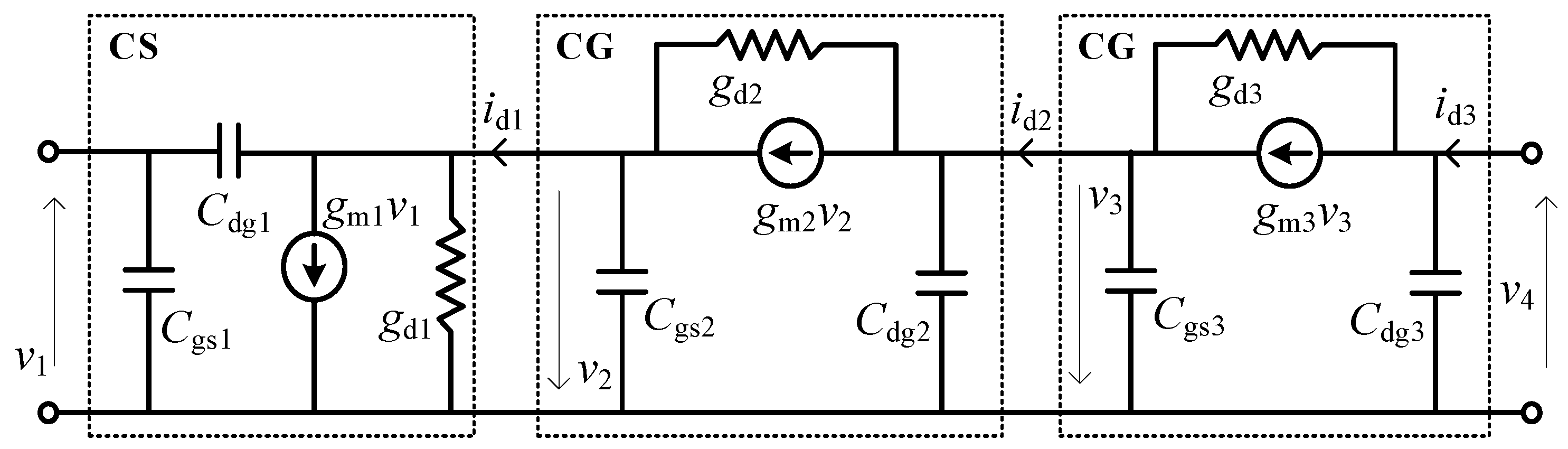
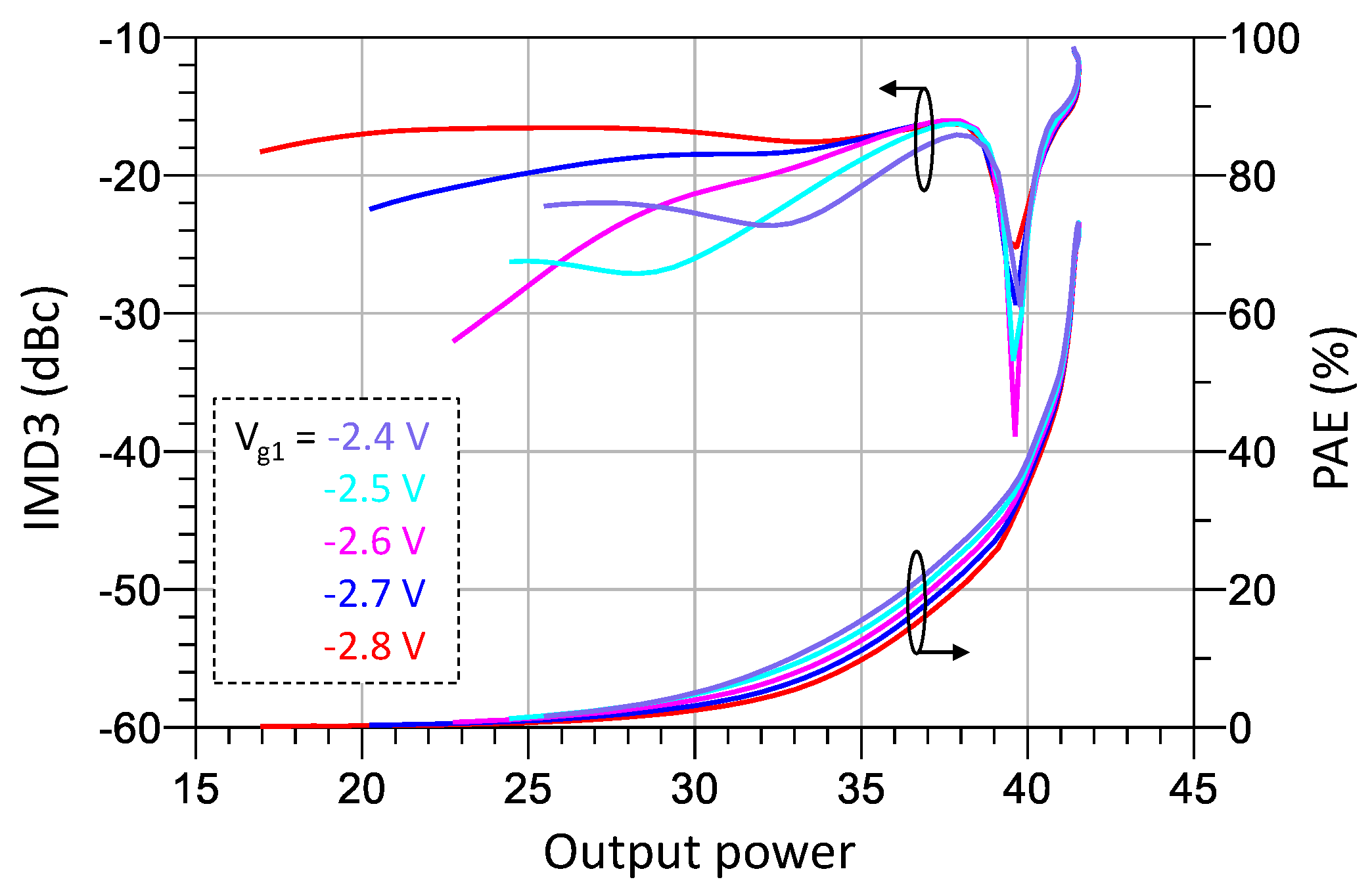
2.2.1. Investigations

Figure 10, Figure 11 and Figure 12 show the investigation of the linearity (IMD3) and efficiency (PAE) of the proposed configuration with respect to the variation of gate bias voltages V g 1 , V g 2 , and V g 3 . As shown in the figures, V g 1 contributes significantly to the change in both IMD3 and PAE, while V g 2 only affects IMD3 at low-power region but it does not affect PAE; V g 3 moderately affects IMD3 in the medium-power region and it affects PAE remarkably in the entire power range. This implies that both IMD3 and PAE can be simultaneously improved by adjusting the gate bias voltages. This is another very promising advantage of the proposed configuration because IMD3 and PAE are hard to improve simultaneously using traditional design methods, as mentioned in the introductory section.

2.2.2. Comparison with Other Configurations

In order for an appropriate comparison of the LS operation, the bias conditions of each transistor of the independently biased configurations, including independently biased cascode and independently biased 3-stack, are individually optimized to achieve their best performance. The conventional configurations including single-stage, conventional cascode, and conventional 3-stack cannot do this due to the lack of the additional bias terminals. The LS investigation is conducted at an operation frequency of 3.5 GHz which is useful for using in next-generation of wireless communication systems. The GaN HEMT LS model is provided by WIN Semiconductor Corp. Figure 13 shows the comparison in output power and power gain among the configurations. Obviously, single-stage and cascode configurations have significantly low power gain and output power compared with that of the 3-stack configurations. The proposed 3-stack configuration has similar output power and power gain as that of the conventional 3-stack one. Both of them have the highest output power and power gain compared with the other configurations. This is because the 3-stack configurations can deliver higher output voltage swing.
It is noted that the efficiency of each configuration is obtained by using a load/source pull technique based on the LS GaN HEMT model to find out their optimum load/source impedances as mentioned previously. These optimum impedances for each configuration are given in Table 2.
Additionally, the bias conditions of each configuration are given in Table 3. In contrast to the SS investigation in which operation condition is set at the class-A, in LS investigation the operation conditions of the transistor are set at a class-AB for the non-linear operation. Along with efficiency, another key performance when designing power amplifier is the linearity.
Although both the 3-stack configurations have similar output power and power gain, the efficiency of the conventional 3-stack one is poorer than that of the proposed 3-stack one, as indicated in Figure 14. As shown in the figure, the proposed 3-stack has superior efficiency among the configurations.In this paper, IMD3 is tested at a center frequency of 3.5 GHz with a frequency spacing of 4 MHz. In Figure 15 the IMD3 performances of the configurations corresponding to their efficiency are shown.
In IMD3 test, the limit level should be at −35 dBc. The figure shows that IMD3 of the single-stage cannot reach this level because it does not use any linearity improvement method. On the other hand, the other configurations can reach this IMD3 level. Table 4 summarizes this comparison. It can be seen in the table that at an IMD3 level of −35 dBc, the proposed 3-stack configuration has highest efficiency of 35% compared with that of the other configurations, by controlling the gate bias voltages. This verifies the advantage of the proposed configuration in term of both efficiency and linearity improvement.
Finally, to demonstrate the advantage of such a proposed independently biased 3-stack circuit structure in terms of bandwidth, the PAE bandwidths of the 5 circuit configurations are compared to each other, as shown in Figure 16 below.
It can be clearly seen in the figure that the proposed 3-stack configuration exhibits superior PAE bandwidth over the others. The PAEs of the single-stage and independently biased casocode configurations drop significantly at both lower and upper frequency regions, while the PAEs of the conventional cascode and conventional 3-stack configurations are severely reduced in both the regions compared with other ones. The proposed configuration can maintain high efficiency in a wide frequency range compared with the other methods.

3. Discussion

This study has proposed a novel independently biased 3-stack GaN HEMT configuration to overcome inherent drawbacks of traditional design methods for both the LNA and PA of tranceiver systems. For the design of the LNA, the proposed configuration becomes an excellent candidate since it exhibits superior stability, isolation, power gain, and noise figure compared with other configurations. Both the power gain and noise figure can be simultaneously improved by an adaptive control of the gate bias voltage of the first transistor. Despite having a slight degradation of power gain and noise figure compared with that of the single-stage and independently biased cascode configurations at the high-frequency region, it still exhibits the best compromise of overall performance. For the design of the PA at an operation frequency of 3.5 GHz, it shows simultaneous improvement of efficiency and linearity by appropriately controlling the gate bias voltages of the individual transistors. The LS performance of the proposed configuration has been compared to that of the other configurations. The compared results indicate that the proposed topology offers the best compromise in efficiency and linearity improvement. Despite having poorer linearity than the independently biased cascode configuration, the proposed topology can deliver better efficiency at the same linearity level. Generally, although the independently biased cascode configuration has the similar ability of independent control of bias condition for each transistor, it cannot efficiently optimize both the SS and LS performance at the same time compared with the proposed configuration. Therefore, the proposed configuration becomes the best choice among the configurations for use in modern wireless communication systems.

Author Contributions

D.M.L. and B.G.D. performed simulation and analyzed the data; H.H.N. contributed analysis tools; D.M.L. and B.G.D. wrote the paper; D.M.L., B.G.D. and H.H.N. modified the paper.

Funding

This research is funded by Vietnam National Foundation for Science and Technology Development (NAFOSTED) under grant number 102.04-2018.14.

Conflicts of Interest

The authors declare no conflict of interest.

References

  1. Shockley, W. Circuit Element Utilizing Semiconductive Material. U.S. Patent 2,569,347, 26 June 1948. [Google Scholar]
  2. Nawa, K.; Iwasaki, M. Darlington Circuit Semiconductor Device. U.S. Patent 4,138,690, 6 February 1979. [Google Scholar]
  3. Andrei, C.; Bentsson, O.; Doerner, R.; Chevtchenko, A.S.; Rudolph, M. Robust stacked GaN-based low-noise amplifier MMIC for receiver applications. In Proceedings of the 2015 IEEE MTT-S International Microwave Symposium, Phoenix, AZ, USA, 17–22 May 2015. [Google Scholar]
  4. Fan, X.; Zhang, H.; Sinencio, E.S. A Noise Reduction and Linearity Improvement Technique for a Differential Cascode LNA. IEEE J. Solid-State Circuits 2008, 43, 588–599. [Google Scholar] [CrossRef] [Green Version]
  5. Hsieh, H.H.; Wang, J.H.; Lu, L.H. Gain-Enhancement Techniques for CMOS Folded Cascode LNAs at Low-Voltage Operations. IEEE Trans. Microw. Theory Tech. 2008, 56, 1807–1816. [Google Scholar] [CrossRef]
  6. Madam, A.; McPartlin, M.C.; Vaillancourt, W.; Cressler, D.J. A 5 GHz 0.95 dB NF Highly Linear Cascode Floating-Body LNA in 180 nm SOI CMOS Technology. IEEE Microw. Wirel. Compon. Lett. 2012, 22, 200–202. [Google Scholar] [CrossRef]
  7. Gilardo, G.; Palmisano, G. Noise figure and impedance matching in RF cascode amplifiers. IEEE Trans. Circuits Syst. II Analog Digit. Signal Process. 1999, 46, 1388–1396. [Google Scholar]
  8. Weber, R.; Cwiklinski, M.; Wagner, S.; Lozar, R.; Massler, H.; Bruckner, P.; Quay, R. A Beyond 110 GHz GaN Cascode Low-Noise Amplifier with 20.3 dBm Output Power. In Proceedings of the 2018 IEEE MTT-S International Microwave Symposium, Philadelphia, PA, USA, 10–15 June 2018. [Google Scholar]
  9. Ulusoy, A.C.; Song, P.; Khan, W.T.; Kaynak, M.; Tillack, B.; Papapolymerou, J.; Cressler, J.D. A SiGe D-Band Low-Noise Amplifier Utilizing Gain-Boosting Technique. IEEE Microw. Wirel. Compon. Lett. 2015, 25, 61–63. [Google Scholar] [CrossRef]
  10. Ding, B.; Yuan, S.; Zhao, C.; Tao, L.; Li, X.; Tian, T. A Ka band CMOS differential LNA with 25 dB gain using neutralized bootstrapped cascode amplifier. IEICE Electron. Express 2018, 6, 1–12. [Google Scholar] [CrossRef]
  11. Liu, Z.; Dong, J.; Chen, Z.; Jiang, Z.; Liu, P.; Wu, Y.; Zhao, C.; Kang, K. A 62–90 GHz High Linearity and Low Noise CMOS Mixer Using Transformer-Coupling Cascode Topology. IEEE Access 2018, 6, 19338–19344. [Google Scholar] [CrossRef]
  12. Ahmadi, M.M. A new modeling and optimization of gain-boosted cascode amplifier for high-speed and low-voltage applications. IEEE Trans. Circuits Syst. I Reg. Pap. 2005, 52, 2327–2334. [Google Scholar] [CrossRef]
  13. Sowlati, T.; Leenaerts, D. A 2.4-GHz 0.18-/spl mu/m CMOS self-biased cascode power amplifier. IEEE J. Solid-State Circuits 2003, 38, 1318–1324. [Google Scholar] [CrossRef]
  14. Fraysse, J.P.; Viaud, J.P.; Campovecchio, M.; Auxemery, P.; Quere, R. A 2 W, high efficiency, 2–8 GHz, cascode HBT MMIC power distributed amplifier. In Proceedings of the 2000 IEEE MTT-S International Microwave Symposium Digest (Cat. No.00CH37017), Boston, MA, USA, 11–16 June 2000. [Google Scholar]
  15. Jin, S.; Park, B.; Moon, K.; Kwon, M.; Kim, B. Linearization of CMOS Cascode Power Amplifiers Through Adaptive Bias Control. IEEE Trans. Microw. Theory Tech. 2013, 61, 4534–4543. [Google Scholar] [CrossRef]
  16. Ko, S.; Lin, J. A Linearized Cascode CMOS Power Amplifier. In Proceedings of the 2006 IEEE Annual Wireless and Microwave Technology Conference, Clearwater Beach, FL, USA, 4–5 December 2006. [Google Scholar]
  17. Kang, S.; Jeong, G.; Hong, S. Study on Dynamic Body Bias Controls of RF CMOS Cascode Power Amplifier. IEEE Microw. Wirel. Compon. Lett. 2018, 28, 705–707. [Google Scholar] [CrossRef]
  18. Ju, I.; Cressler, J.D. A Highly Efficient X-Band Inverse Class-F SiGe HBT Cascode Power Amplifier With Harmonic-Tuned Wilkinson Power Combiner. IEEE Trans. Circuits Syst. II Express Briefs 2017, 65, 1609–1613. [Google Scholar] [CrossRef]
  19. Jeong, G.; Joo, T.; Hong, S. A Highly Linear and Efficient CMOS Power Amplifier With Cascode–Cascade Configuration. IEEE Microw. Wirel. Compon. Lett. 2017, 27, 596–598. [Google Scholar] [CrossRef]
  20. Moon, J.S.; Grabar, R.; Brown, D.; Rodriguez, I.A.; Wong, D.; Schmitz, A.; Fung, H.; Chen, P.; Kang, J.-C.; Kim, S.; et al. >70% Power-Added-Efficiency Dual-Gate, Cascode GaN HEMTs Without Harmonic Tuning. IEEE Microw. Wirel. Compon. Lett. 2016, 37, 272–275. [Google Scholar] [CrossRef]
  21. Armijo, C.T.; Meyer, R.G. A new wide-band Darlington amplifier. IEEE J. Solid-State Circuits 1989, 24, 1105–1109. [Google Scholar] [CrossRef]
  22. Kuo, C.W.; Chiou, H.K.; Chung, H.Y. An 18 to 33 GHz Fully-Integrated Darlington Power Amplifier with Guanella-Type Transmission-Line Transformers in 0.16 μm CMOS Technology. IEEE Microw. Wirel. Compon. Lett. 2013, 23, 668–670. [Google Scholar] [CrossRef]
  23. Kobayashi, K.W.; Umemoto, D.K.; Velebir, J.R.; Oki, A.K.; Streit, D.C. Ntegrated complementary HBT microwave push-pull and Darlington amplifiers with p-n-p active loads. IEEE J. Solid-State Circuits 1993, 28, 1011–1017. [Google Scholar] [CrossRef]
  24. Hu, S.; Yu, S.; Hu, Y.; Wang, Z.; Zhou, B.; Cai, Z.; Guo, Y. A 0.2–6 GHz Linearized Darlington-cascode broadband power amplifier. IEICE Electron. Express 2018, 15, 1–8. [Google Scholar] [CrossRef]
  25. Lin, Y.-A.; Yeh, Y.-C.; Chang, H.-Y. A 27-GHz 45-dB SFDR track-and-hold amplifier using modified darlington amplifier and cascoded SEF in 0.18-μm SiGe process. In Proceedings of the 2017 IEEE MTT-S International Microwave Symposium, Honololu, HI, USA, 4–9 June 2017. [Google Scholar]
  26. Nguyen, D.P.; Stameroff, N.A.; Pham, A.V. A 1.5–88 GHz 19.5 dBm Output Power Triple Stacked HBT InP Distributed Amplifier. In Proceedings of the 2017 IEEE MTT-S International Microwave Symposium, Honololu, HI, USA, 4–9 June 2017. [Google Scholar]
  27. Tarar, M.M.; Beucher, T.; Qayyum, S.; Negra, R. Efficient 2–16 GHz Flat-Gain Stacked Distributed Power Amplifier in 0.13 μm CMOS using Uniform Distributed Topology. In Proceedings of the 2017 IEEE MTT-S International Microwave Symposium, Honololu, HI, USA, 4–9 June 2017. [Google Scholar]
  28. Wu, H.; Liao, X.; Wang, C.; Chen, Y.; Hua, Y.; Hu, Y.; Lv, J.; Tong, W. A 4-10 GHz Fully-integrated Stacked GaAs pHEMT Power Amplifier. In Proceedings of the 2017 IEEE MTT-S International Microwave Symposium, Honololu, HI, USA, 4–9 June 2017. [Google Scholar]
  29. Takagi, Y.; Takayama, Y.; Ishikawa, R.; Honjo, K. A High-Efficiency Low-Distortion Cascode Power Amplifier Consisting of Independently Biased InGaP/GaAs HBTs. IEICE Trans. Electron. 2014, 97, 58–64. [Google Scholar] [CrossRef]
  30. Luong, D.M.; Takayama, Y.; Ishikawa, R.; Honjo, K. Power gain performance enhancement of independently biased heterojunction bipolar transistor cascode chip. Jpn. J. Appl. Phys. 2015, 54, 1–8. [Google Scholar] [CrossRef]
  31. Luong, D.M.; Takayama, Y.; Ishikawa, R.; Honjo, K. Microwave Characteristics of an Independently Biased 3-Stack InGaP/GaAs HBT Configuration. IEEE Trans. Circuits Syst. I Reg. Pap. 2016, 64, 3487–3495. [Google Scholar] [CrossRef]
  32. Luong, D.M.; Nguyen, H.H.; Bach, G.D.; Ta, C.H. Design of An Independently Biased Cascode GaN HEMT Microwave Power Amplifier. In Proceedings of the International Conference on Advanced Technologies for Communications 2018 (ATC2018), Ho Chi Minh City, Vietnam, 18–20 October 2018. [Google Scholar]
  33. Advanced Design System (ADS). Available online: https://www.keysight.com/en/pc-1297113/advanced-design-system-ads?&cc=VN&lc=eng (accessed on 4 February 2019).
  34. WIN Semiconductors Corp. Available online: https://www.winfoundry.com/ (accessed on 4 February 2019).
  35. Pozar, D.M. Microwave Engineering, 4th ed.; John Wiley & Son: Hoboken, NJ, USA, 2012. [Google Scholar]
Figure 1. Circuit configurations: (a) single-stage; (b) conventional cascode; (c) independently biased cascode; (d) conventional 3-stack; (e) independently biased 3-stack.
Applsci 09 01510 g001
Figure 2. Simulation setup for S-parameters simulation in Keysight advanced design system (ADS).
Applsci 09 01510 g002
Figure 3. Small-signal equivalent circuit of the proposed 3-stack GaN high-electron-mobility transistor (HEMT) configuration.
Applsci 09 01510 g003
Figure 4. Power gain and noise figure characteristic of the proposed configuration.
Applsci 09 01510 g004
Figure 5. Reverse isolation and stability characteristic of the proposed configuration.
Applsci 09 01510 g005
Figure 6. Reverse isolation comparison among configurations.
Applsci 09 01510 g006
Figure 7. Stability comparison among configurations.
Applsci 09 01510 g007
Figure 8. Power gain comparison among configurations.
Applsci 09 01510 g008
Figure 9. Noise figure comparison among configurations.
Applsci 09 01510 g009
Figure 10. Large-signal (LS) investigation with V g 1 variation.
Applsci 09 01510 g010
Figure 11. LS investigation with V g 2 variation.
Applsci 09 01510 g011
Figure 12. LS investigation with V g 3 variation.
Applsci 09 01510 g012
Figure 13. Output power and power gain characteristic.
Applsci 09 01510 g013
Figure 14. Efficiency characteristic.
Applsci 09 01510 g014
Figure 15. Linearity (IMD3) characteristic.
Applsci 09 01510 g015
Figure 16. Power added efficiency (PAE) bandwidth comparison among configurations.
Applsci 09 01510 g016
Table 1. Bias conditions of the configurations for small-signal (SS) investigations.
Configurations V g 1 V g 2 V g 3 V d 1 V d 2 V d 3
Single-stage−2 VXX44 VXX
Conventional cascode−2 V−2 VXX44 VX
Independently biased cascode−2 V−2 V−2 V5 V44 VX
Conventional 3-stack−2 V−2 V−2 VXX44 V
Independently biased 3-stack−2 V−2 V−2 V1 V3.5 V44 V
Table 2. Optimum source and load impedances of the compared configurations.
ConfigurationsSource Impedance ( Ω )Load Impedance ( Ω )
Single-stage22.3 + j31.2233 + j273
Conventional cascode56 + j293223.2 + j250
Independently biased cascode56 + j293223.2 + j250
Conventional 3-stack55.9 + j101179 + j273
Independently biased 3-stack55.9 + j101179 + j273
Table 3. Bias condition of configurations for large-signal (LS) investigation.
Configurations V g 1 V g 2 V g 3 V d 1 V d 2 V d 3
Single-stage−2.6 VXX44 VXX
Conventional cascode−2.6 V−2.6VX44 VXX
Independently biased cascode−2.6 V−2.6 VX6 V44 VX
Conventional 3-stack−2.6V−2.6 V−2.6 VXX44 V
Independently biased 3-stack−2.6 V−2.6 V−2.6 V5 V4 V44 V
Table 4. Summary of linearity and efficiency performance.
ConfigurationsIMD3 LevelPAE
Single-stage−35 dBcX
Conventional cascode−35 dBc4.5%
Independently biased cascode−35 dBc22.8%
Conventional 3-stack−35 dBc25%
Independently biased 3-stack−35 dBc35%

