Article

Power and Signal-to-Noise Ratio Optimization in Mesh-Based Hybrid Optical Network-on-Chip Using Semiconductor Optical Amplifiers

1
Department of Semiconductor and Display Engineering, Sungkyunkwan University, Suwon 16419, Gyeonggi-Do, Korea
2
Eyenix Co., Suwon 16690, Gyeonggi-Do, Korea
3
Department of Electrical and Computer Engineering, Sungkyunkwan University, Suwon 16419, Gyeonggi-Do, Korea
*
Author to whom correspondence should be addressed.
Appl. Sci. 2019, 9(6), 1251; https://doi.org/10.3390/app9061251
Submission received: 3 March 2019 / Revised: 21 March 2019 / Accepted: 22 March 2019 / Published: 25 March 2019

Abstract

:
To address the performance bottleneck in metal-based interconnects, hybrid optical network-on-chip (HONoC) has emerged as a new alternative. However, as the size of the HONoC grows, insertion loss and crosstalk noise increase, leading to excessive laser source output power and performance degradation. Therefore, we propose a low-power scalable HONoC architecture by incorporating semiconductor optical amplifiers (SOAs). An SOA placement algorithm is developed considering insertion loss and crosstalk noise. Furthermore, we establish a worst-case crosstalk noise model of SOA-enabled HONoC and induce optimized SOA gains with respect to power consumption and performance, respectively. Extensive simulations for worst-case signal-to-noise ratio (SNR) and power consumption are conducted under various traffic patterns and different network sizes. Simulation results show that the proposed SOA-enabled HONoC architecture and the associated algorithm help sustain the performance as network size increases without additional laser source power.

Graphical Abstract

1. Introduction

As multicore systems-on-chips (SoCs) have become mainstream as chips suffer from diminishing returns of miniaturization and the power wall, a new high-performance on-chip network architecture is needed to overcome the physical limitations of metal interconnects [1,2]. A hybrid optical network-on-chip (HONoC) in which the electrical and optical layers are combined, using silicon photonics technology, is emerging as a new alternative for replacing metallic interconnects [3]. The HONoC uses the optical layer to transmit massive data and uses the electrical layer to send control packets or small-size data. As the number of cores in the system increases, the network-size-scalable architecture is highly desirable. The widely-known mesh topology is chosen due to its simplicity and regularity in terms of layout, after considering the advantages of the topology revealed by existing studies on mesh-based HONoCs [4,5,6].
For reliable communication, the optical signal power arriving at the receiver should be higher than the sensitivity of the photodetector. Because of the significant insertion loss in large-scale HONoCs due to the accumulated microring resonator (MR) drops and waveguide crossings, the laser source output power should be increased. As the laser source is the most power-consuming device among the optical devices, the insertion loss acts as a dominant factor for the overall power consumption of the HONoC.
Lan et al. [7] suggested the dynamic laser power control to reduce the power consumption of the ONoC. However, adaptive laser power management demands complicated control and exhibits limited power efficiency. Moreover, even if the power efficiency of the chip is increased by reducing the laser source power, reliable communication is not guaranteed under high crosstalk noise environments with heavy data traffic cases [8].
We propose a low-power scalable HONoC architecture by deploying semiconductor optical amplifiers (SOAs) and the closely related SOA placement algorithm considering the insertion loss and crosstalk noise change caused by SOA deployment. An analytic worst-case crosstalk noise model is developed to find the optimized SOA gain that minimizes crosstalk noise and to investigate the effect of SOAs on worst-case signal-to-noise ratio (SNR) in HONoC. Considering the relationship between SOA placement and worst-case insertion loss, we calculate the minimum SOA gain for laser source power savings.
The remainder of this paper is organized as follows. Section 2 briefly provides related research and background information regarding insertion loss and crosstalk noise. In Section 3, we introduce the optical router and the SOA model and present a constraint optimization problem for implementing an SOA-enabled HONoC. In Section 4, to solve the constraint optimization problem, we propose an SOA placement algorithm and analyse the worst-case crosstalk noise. Based on the crosstalk noise model, the correlation between the SOA and the SNR is analysed. We also calculate the minimum SOA gain to apply laser source power independent of the longest path. In Section 5, we evaluate and compare the worst-case SNR and power consumption of SOA-enabled HONoC. We draw the conclusion in Section 6.

2. Related Work

2.1. Insertion Loss

The worst-case insertion loss is the dominant factor in determining the laser source output power to ensure reliable communication in the HONoC. The two major causes of insertion loss due to MR drop (Figure 1a) and waveguide crossings (Figure 1b) were reported to be 0.5–1.5 dB and 0.04–0.12 dB, respectively [9,10,11,12,13].
The received signal power should be higher than the sensitivity of the photodetector. Therefore, the relationship between the laser source power ( P l a s e r ) , worst-case insertion loss ( P w o r s t _ I L ) and sensitivity of the photodetector ( P s e n s i t i v i t y ) can be expressed as
P l a s e r P w o r s t I L + P s e n s i t i v i t y ,
where P s e n s i t i v i t y has been reported as approximately −20 dBm [14].
Other types of optical signal power losses considered at the system-level analysis are as follows:
(1)
The waveguide propagation loss is −0.274 dB/cm [15].
(2)
The MR through loss is smaller than the MR drop loss by two orders of magnitude [16].
Given that these factors are minor in comparison to major insertion losses, most on-chip network architecture studies focus on reducing the insertion losses caused by MR drops and waveguide crossings.

2.2. Crosstalk Noise

Crosstalk noise is an unavoidable characteristic of photonic devices. Sanchis et al. proposed a method for selecting the optimal crossing angle of the waveguide to reduce the crosstalk [17]. Chen et al. proposed multimode-interference (MMI)-based waveguide crossing instead of plain waveguide crossing for reducing signal power loss [18]. They designed a compact structure to minimize the crosstalk at the device level.
Despite these efforts, leakage signals that act as crosstalk cannot be ignored due to their accumulation. Especially, crosstalk noise should be considered as network size increases. In a network-level, Xie et al. analysed crosstalk noise and worst-case SNR through a formal approach in a mesh-based ONoC [19]. According to their research, crosstalk noise causes severe performance degradation and limits the scalability of the HONoC architectures.
Studies on crosstalk noise have been conducted with respect to router architectures, network topologies and traffic patterns [20,21,22]. On the other hand, there are few studies regarding crosstalk noise when integrating the SOA. The SOA can significantly reduce insertion loss; however, it can also increase crosstalk noise. In this regard, we analyse the correlation between the SOA, insertion loss and crosstalk noise and then propose a methodology to efficiently compensate insertion loss and minimize crosstalk noise.

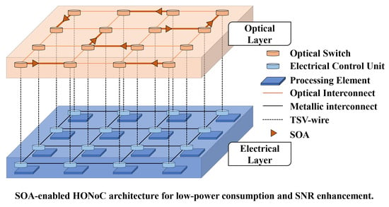
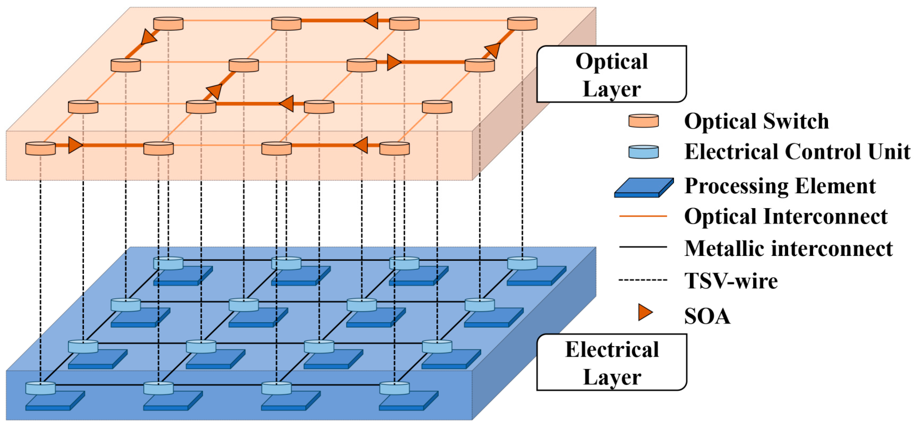
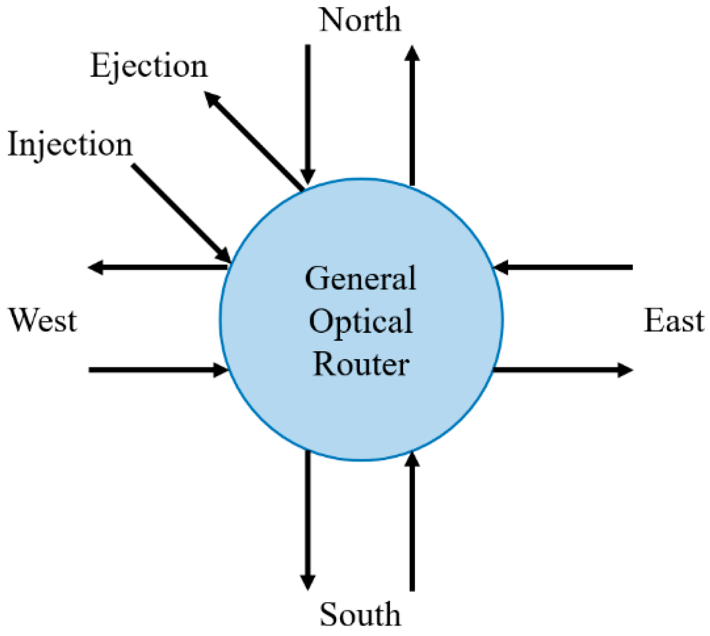
3. SOA-Enabled HONoC Architecture

Our proposed architecture, as shown in Figure 2, is a mesh-based HONoC with integrated SOAs and consists of two layers. The electrical layer controls the optical layer while transmitting control packets and small-size data through packet switching. Before the optical data transaction between the cores starts, the routing path should be setup in advance through the electrical layer. During the path setup process, the ON/OFF state of SOAs and MRs located in the path are determined and the SOA gain is controlled by adjusting the bias current applied to the SOA.
In the optical layer, data transaction is performed using circuit switching due to the absence of optical storage. The SOAs can amplify the optical signal power attenuated by photonic devices in the routing path. The SOAs outside of the routing path are in the OFF state and absorb the optical signal power. In this study, the expected effects of integrating the SOA with the mesh-based HONoC are as follows:
  • The SOA compensates for the insertion loss by amplifying the optical signal and reduces the burden of the laser source to reduce the total power consumption of the HONoC.
  • An appropriate SOA gain can prevent the SNR degradation problem of the longest path due to the network size growth of the mesh-based HONoC.

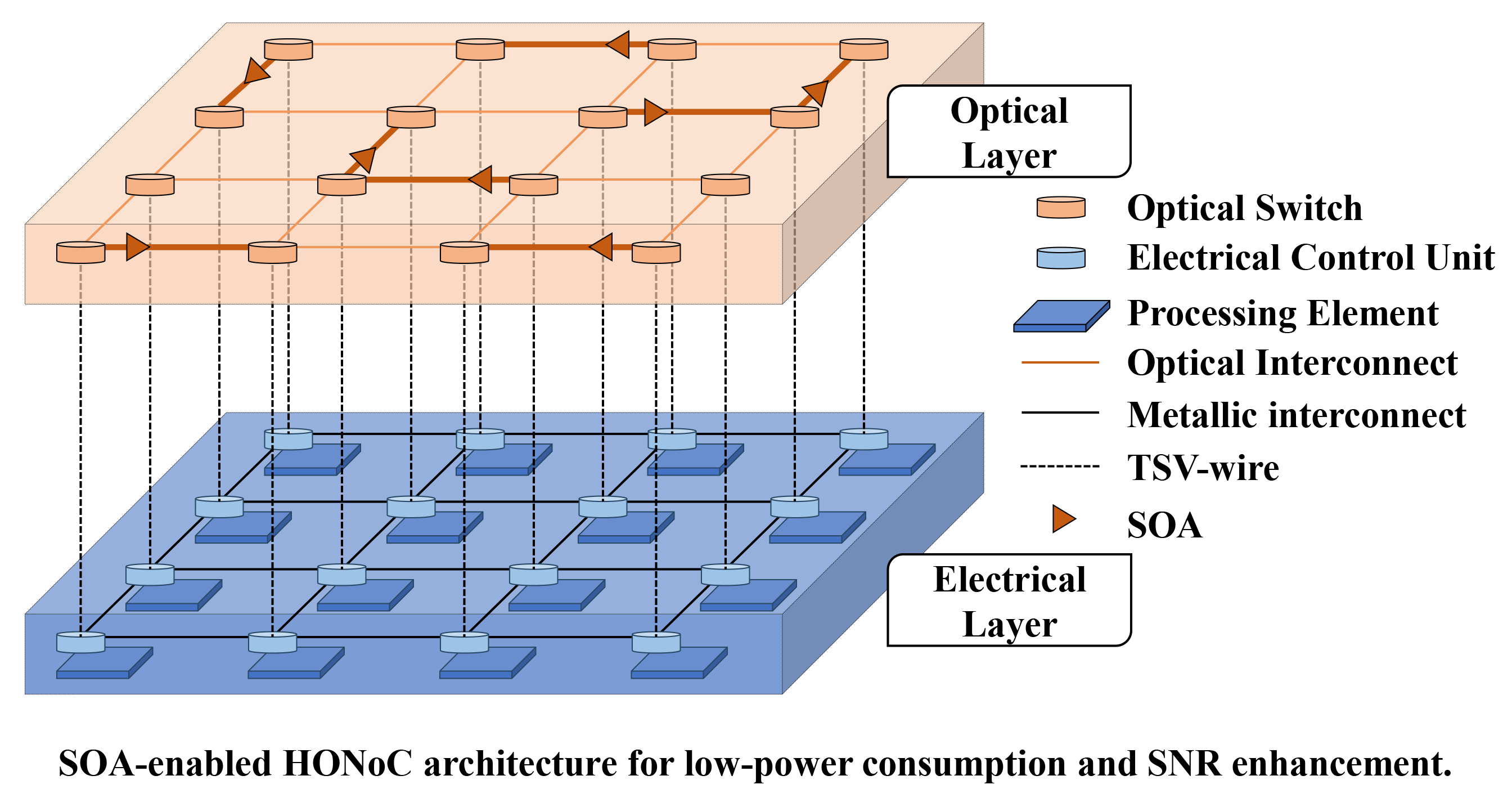
3.1. Optical Router Model

The 5 × 5 general optical router for mesh-based HONoC, as shown in Figure 3, consists of the following five ports: Injection/Ejection, North, East, South and West. The ONoC parameters in this analysis are based on the study conducted by Xie et al. [19], which presented the formal analytic models of insertion loss and crosstalk noise for mesh-based HONoCs.
Optical signals can traverse from the i th port to the j th port and the value of i and j varies from 0 to 4: 0 denotes the Injection/Ejection port and 1–4 denote the North, East, South and West ports, respectively. P i n i denotes the optical power coming into the i th port and L i , j ( x , y ) is the insertion loss from the i th port to the j th port in the optical router located at ( x , y ) in the mesh-based HONoC. P i , j ( x , y ) , defined in (2), is the optical power when going from the i th port to the j th port in the optical router R ( x , y ) .
P i , j ( x , y ) =   P i n L i , j ( x , y )   i ,   j { 0 ,   ,   4 } ,     x { 1 ,   ,   m } ,     y { 1 ,   ,   n }
N i , j ( x , y ) , calculated in (3), denotes the crosstalk noise introduced into the optical router located at ( x , y ) in the mesh-based HONoC and K i , j , k is the crosstalk noise introduced into the k th port when the optical signal travels from the i th port to the j th port.
N i , j ( x , y ) =   P i n 0 ( x , y ) K i , j , 0 +   P i n 1 ( x , y ) K i , j , 1 + P i n 2 ( x , y ) K i , j , 2 + P i n 3 ( x , y ) K i , j , 3 + P i n 4 ( x , y ) K i , j , 4
The SNR is the ratio of the signal power to the noise power and can be written as
SNR = 10 log ( P S P N ) ,
where P S is the power of the optical signal and P N is the power of noise.

3.2. Semiconductor Optical Amplifier

The SOA is mainly used for amplifying the input optical signals, switching and frequency conversion [23]. The SOA can be integrated into a CMOS-compatible chip and thus can be implemented in the HONoC by using silicon photonics technology. The operating principle of the SOA is that electrons and holes are injected into the n-type region and the p-type region respectively, causing population inversion in the active region. Population inversion leads to stimulated emission and therefore, a photon injected into the SOA triggers another photon with the same phase, wavelength and direction. Optical gain is obtained through this process.
In the active region, the gain per unit length of the SOA is called material gain ( g ) and is expressed in (5a) as a function of wavelength ( λ ) and current ( I ). As L increases, the SOA gain ( G ) increases accordingly. Here, g and G are in cm 1 and dB units, respectively.
g ( λ , I ) = [ Γ a 1 n 0 { I I 0 1 } α ] [ 1 2 ( λ 1570 ) 2 Δ λ 2 ]
G ( λ , I ) = 10 log 10 ( e L g ( λ ,     I ) )
Γ , a 1 , n 0 , L , I 0 , α and Δ λ depend on the material and the structural characteristics of the SOA; the definitions and values of each parameter are shown in Table 1 [24]. As in Equation (5), the SOA gain is proportional to the current. The operating voltage of the SOA and the wavelength are assumed to be 1.5 V and 1550 nm, respectively. In addition, it takes 20–50 ps for the SOA to reach the target gain. The SOA model in this study is simplified for the purpose of system-level analysis; therefore, the physical effect of the amplified spontaneous emission (ASE) introduced by the SOAs is not considered. Although ASE cannot be ignored in physical implementations with contemporary silicon photonics technology, this study focuses on the emerging architecture with a matured manufacturing process that enables feasible on-chip SOAs, assuming a negligible ASE compared to the cumulated crosstalk noise. Additionally, it is also assumed that the placement of SOAs can be over-layered on waveguides in the physical layout; therefore, SOAs do not affect the spaces between optical routers.

3.3. Constrained Optimization Problem in SOA-Enabled HONoC

In the HONoC, laser source power mainly depends on the total loss experienced by the optical signal in the longest path. The laser source power level is determined to ensure that the signal power at the receiver is greater than the sensitivity of the photodetector. Therefore, we reduce the burden of the laser source power by using the SOA, which is easy to integrate and of relatively low processing cost. Appropriately placing SOAs across the signal path is an effective way to save the laser source output power in large-scale HONoCs if the additional power consumption of SOAs is reasonably smaller than the reduced amount of the laser source power.
As the total power consumption of the SOA-enabled HONoC depends on the location, spacing and number of SOAs, an efficient SOA placement is needed to achieve the goal. Furthermore, the SOA placement also affects the worst-case SNR because SOAs can amplify the crosstalk noise power as well as the desired optical signal power. Therefore, the constrained optimization problem for implementing the SOA-enabled HONoC in an m × n mesh is defined as follows:
Minimize :   t o t a l P l a s e r +   t o t a l P S O A
Subject   to :   P s e n s i t i v i t y m i n     { P L ( x 0 , y 0 ) ( x 1 , y 1 ) S O A }
m i n     { S N R ( x 0 , y 0 ) ( x 1 , y 1 ) } m i n     { S N R ( x 0 , y 0 ) ( x 1 , y 1 ) S O A }
x 0 ,   x 1 { 1 ,   ,   m } ,     y 0 ,   y 1 { 1 ,   ,   n }
Here, P l a s e r is the laser source power consumption of the SOA-enabled HONoC, P S O A is the total power consumption of the SOAs, P s e n s i t i v i t y   is the sensitivity of the photodetector, P L ( x 0 , y 0 ) ( x 1 , y 1 ) S O A is the power loss of the optical signal traveling from the router ( x 0 , y 0 ) to the router ( x 1 , y 1 ) in the SOA-enabled HONoC, S N R ( x 0 , y 0 ) ( x 1 , y 1 ) is the SNR of the path from the router ( x 0 , y 0 ) to the router ( x 1 , y 1 ) in the conventional mesh-based HONoC and S N R ( x 0 , y 0 ) ( x 1 , y 1 ) S O A is the SNR of the path from the router ( x 0 , y 0 ) to the router ( x 1 , y 1 ) in the mesh-based HONoC with SOAs.

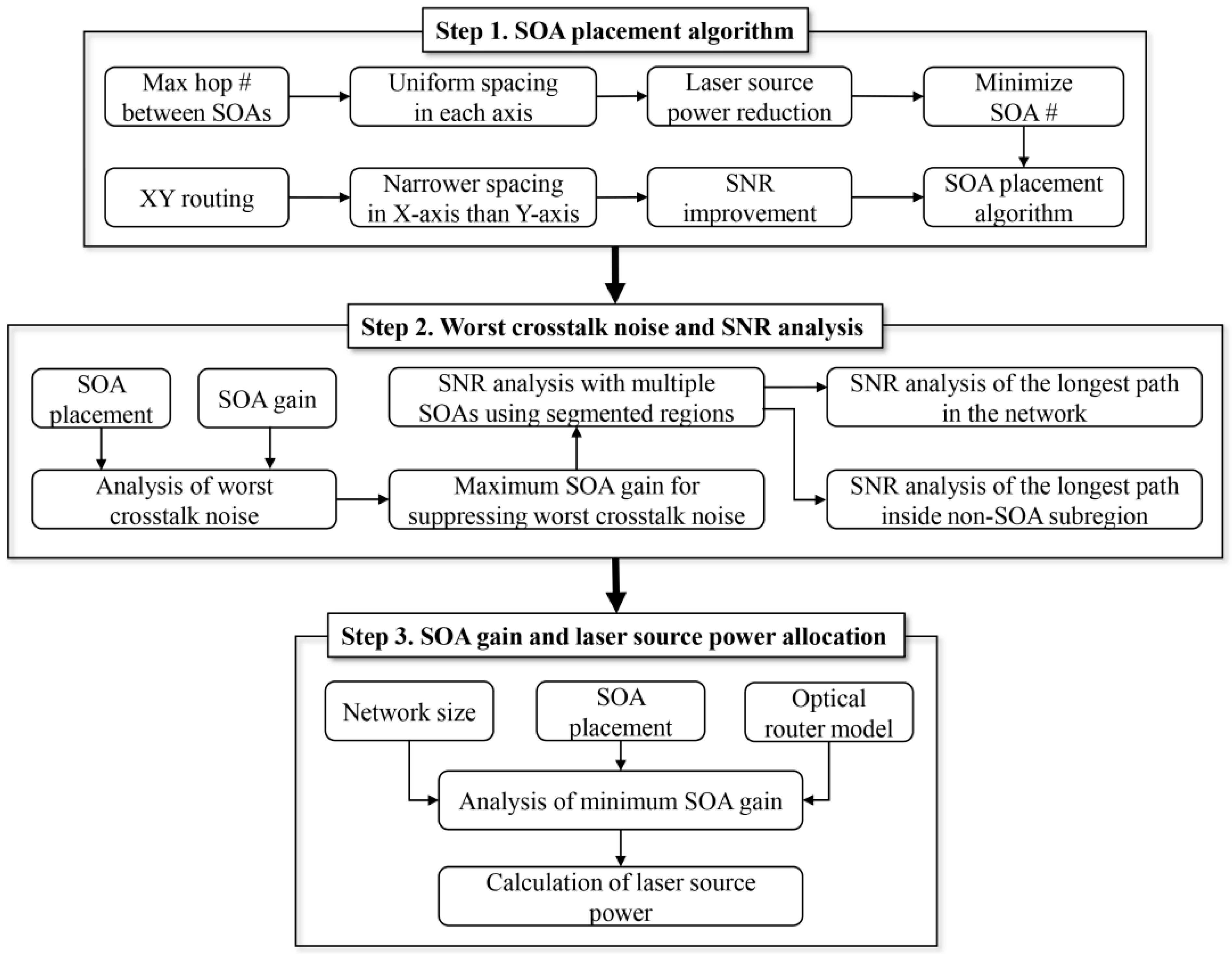
4. Design Methodology for SOA-Enabled HONoC

As mentioned in Section 3.3, the insertion loss problem exacerbates as the network size scales up. On the other hand, the SOA placed to compensate for the insertion loss might adversely affect the SNR caused by unintended crosstalk noise amplification. Therefore, SOA placement considering the routing algorithm should be performed in terms of SNR. In this regard, we devise a design methodology of the SOA-enabled HONoC when XY routing is used in the mesh topology. XY routing has been reported to realize the best performance in terms of bandwidth, latency, load balancing and insertion loss in mesh-based HONoC [5].
The proposed methodology for the SOA-enabled HONoC comprises three steps, as shown in Figure 4. In step 1, we propose an SOA placement algorithm considering insertion loss and SNR. In step 2, the worst-case crosstalk noise due to the SOA placement and the SOA gain to be realized to suppress the crosstalk noise amplification are presented. Based on the SNR analysis with segmented regions, we compare the SNR of the longest path according to the SOA gain and analyse the path in which SNR degradation occurs even if the SOA gain is controlled. In step 3, the algorithm for finding the minimum required SOA gain is developed to allocate the laser source output power independent of the network size.

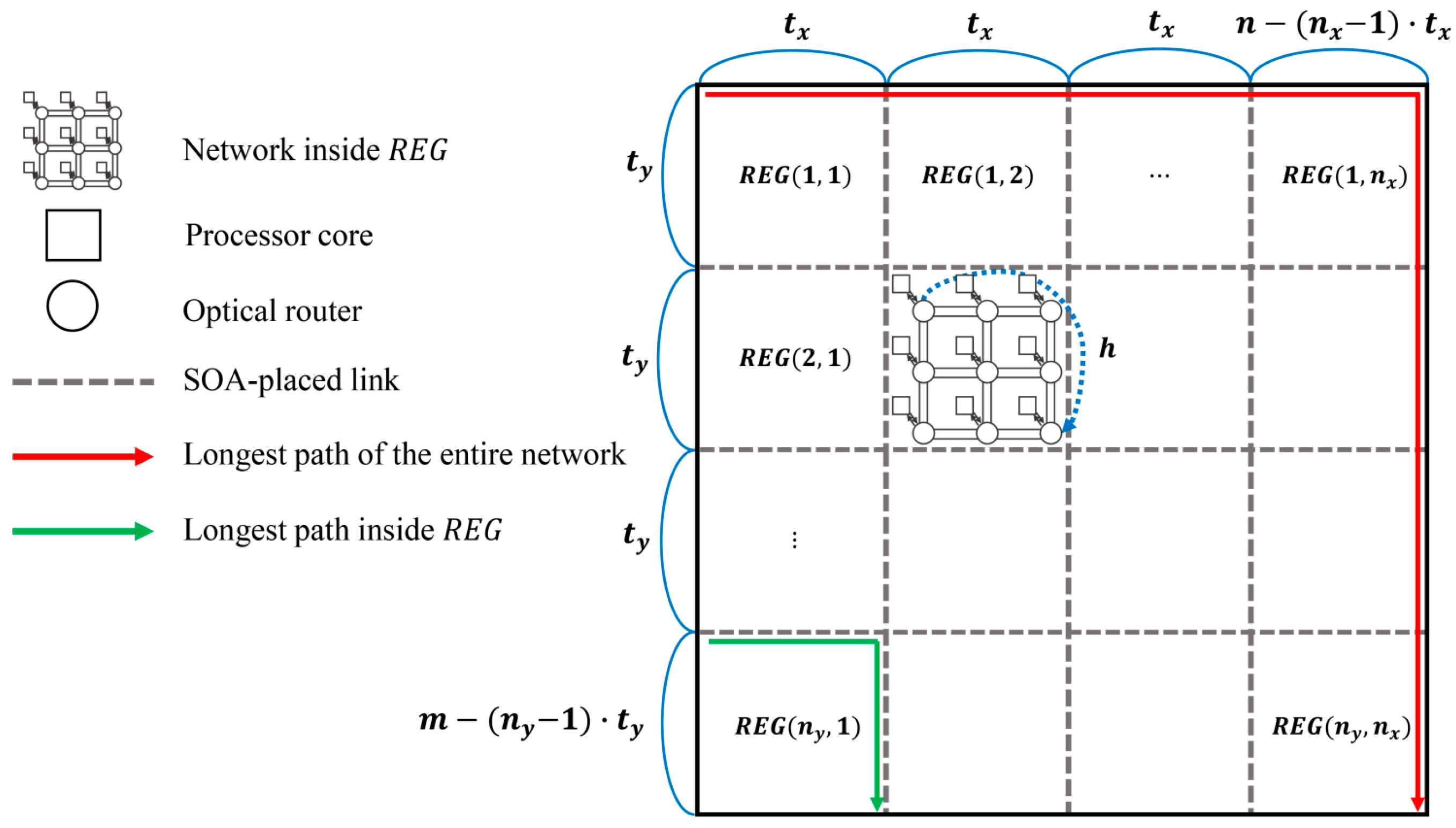
4.1. SOA Placement Algorithm for Laser Source Power Saving and SNR Enhancement

The SOA gain modelling in Equation (5) shows that using a single SOA is superior to using multiple SOAs in that it uses less bias current to obtain the same gain, as described in Equation (7).
G ( I t o t a l ) > i = 1 n G ( I i ) ,     I t o t a l = i = 1 n I i  
In addition to the gain efficiency of the SOA, the small number of SOAs with high gain is advantageous in terms of the area in which the SOA devices and control units are placed. However, this strategy should be validated. As the worst-case insertion loss determines the output power of laser sources and even one SOA has impact on various routing paths, an effective SOA placement rule is needed to reduce the laser source power using the appropriate number of SOAs. Considering the insertion loss due to the SOA placement in the routing path, the power consumption of the HONoC can be effectively reduced by equalizing the maximum number of hops that do not pass through the SOA in all routing paths. We denote this maximum hop count without SOAs as h , which is determined by t x and t y , indicating the SOA spacing on the X-axis and Y-axis, respectively.
The accumulated crosstalk noise power at the destination depends on not only the number of SOAs but also the location of the SOAs. For example, as shown in Figure 5, the crosstalk power increases when the SOA is placed nearer to the destination rather than the source. In other words, to minimize the crosstalk power amplified through the SOAs in the optical signal path, SOA should be placed close to the source. In the mesh-based HONoC with XY routing, the optical signal is transmitted along the Y-axis after the X-axis. Hence, placing more SOAs on the X-axis is preferred to Y-axis in terms of SNR. Accordingly, we propose the SOA placement algorithm as follows. In this study, it is assumed that all SOA gains are the same for the convenience of design and analysis of the network.
Algorithm 1. SOA Placement for Laser Source Power Saving and SNR Improvement
Input: mesh size ( m , n ), maximum hop count of possible paths without SOAs ( h )
Output: number of SOAs ( n S O A ), SOA spacing of X-axis and Y-axis ( t x , t y )
1: n S O A = ( n 1 ) / 1 + ( m 1 ) / ( h + 1 )
2:For i from 1 to h + 1 do
3:   j = h + 2 i
4:   n [ i ] = ( n 1 ) / i + ( m 1 ) / j
5:  If n [ i ] < n S O A then
6:     n S O A = n [ i ]
7:     t = i
8:  End if
9:End for
10: t x = t ,   t y = h + 2 t , n S O A = m · t x + n · t y
11:For i from t x to n 1 do
12:  For j from 1 to m do
13:    Allocate SOA at east link of R( j ,   i )
14:     j = j + 1
15:  End for
16:   i = i + t x
17:End for
18:For i from t y to m 1 do
19:  For j from 1 to n do
20:    Allocate SOA at south link of R( i ,   j )
21:     j = j + 1
22:  End for
23:   i = i + t y
24:End for
In Algorithm 1, the optimal SOA spacing in the X-axis ( t x ) and that in the Y-axis ( t y ) are selected according to the maximum number of hops among the possible routing paths without SOAs ( h ). Therefore, the total number of SOAs placed in the network depends on the possible combinations of t x and t y with a consistent h . To minimize the additional power consumption of the SOAs, use of the smallest number of SOAs should be pursued. If there are several cases with the same number of SOAs, the narrowest X-axis spacing is chosen to improve the SNR (lines 1–10). After the spacing of the SOAs is determined, SOAs are placed on the link of the corresponding router (lines 11–23).

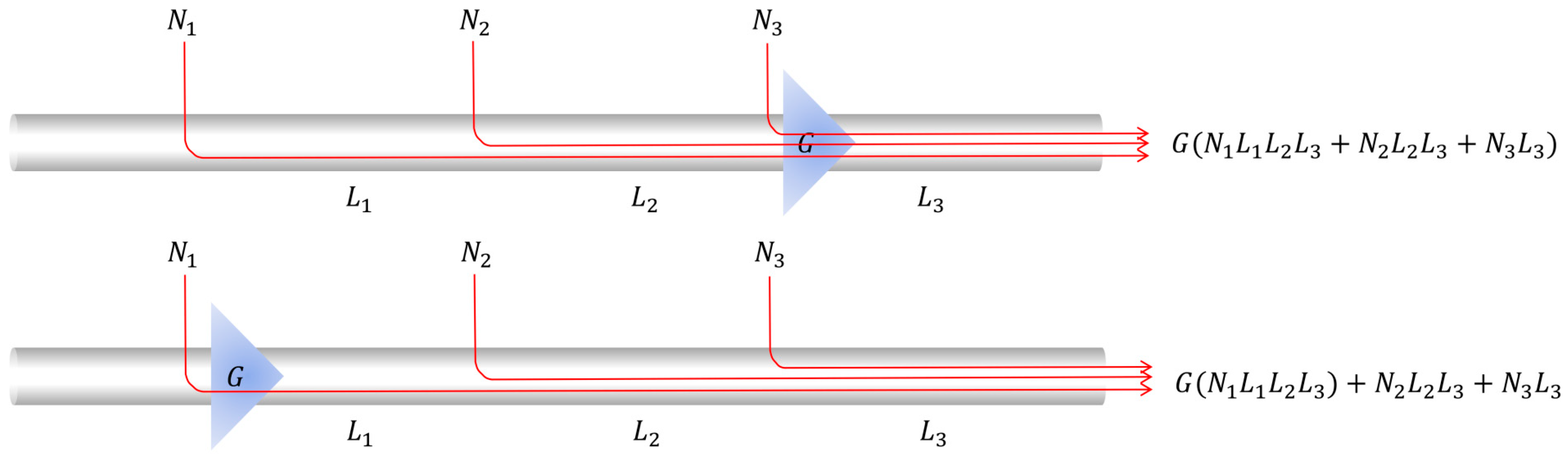
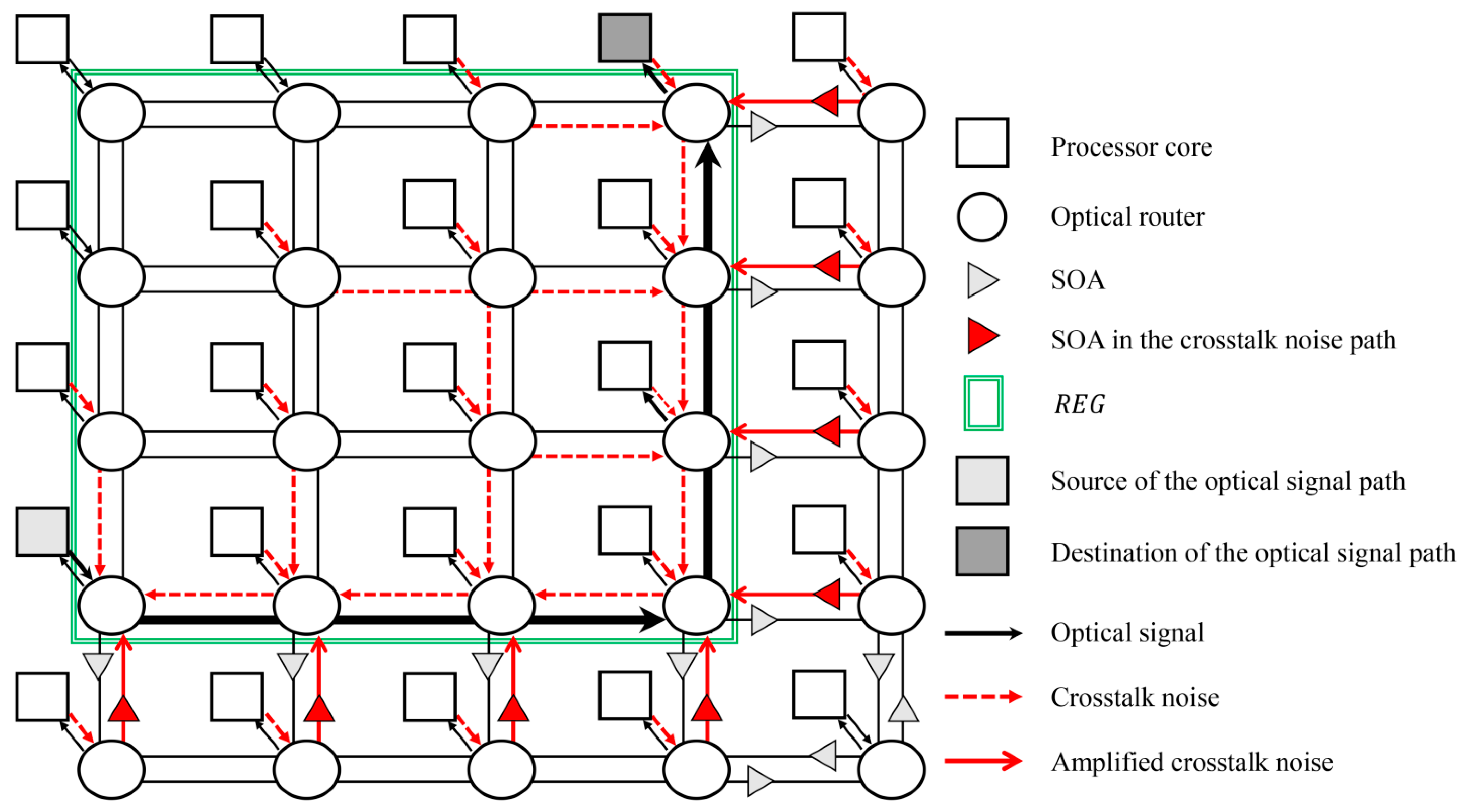
4.2. Worst-Case Crosstalk Noise and SNR Analysis

For the analysis of the worst-case SNR in the proposed architecture, we use several definitions as follows:
  • n r : the total number of routers in the optical signal path
  • n s : the total number of SOAs in the optical signal path
  • t i : the number of the routers between the i th SOA and the ( i 1 ) th SOA in the optical signal path ( t 0 = 0 ,   t n s + 1 = ( #   of   routers   between   the   last   SOA   and   the   destination ) )
  • P N i : the crosstalk noise introduced into the i th router in the optical signal path
  • L : router loss, G : SOA gain, K : crosstalk noise coefficient
To simplify the worst-case SNR equations, we make the following assumptions
  • The insertion loss and the crosstalk noise coefficient are the same regardless of ports. ( L i , j = L , K i , j , n = K )
  • The mesh size is m × m .
As the crosstalk noise introduced into each router is also amplified by the corresponding SOAs in the optical signal path, these effects are reflected in the SNR as in (8).
S N R = 10 log ( P S G n s L n r i = 0 n s G n s i j = T i + 1 T i + 1 ( P N j L n r j ) )   where   T i = k = 0 i t k
As shown in Equation (8), it is inevitable that the crosstalk noise introduced into the optical signal passes through the SOAs located in the signal path. Therefore, to maximize the SNR, the worst crosstalk candidate must be suppressed before it leaks into the desired optical signal path.
The dominant crosstalk power is mainly caused by the crosstalk noise coming from the nearest router in conventional HONoCs. However, in the SOA-integrated HONoC, the worst crosstalk candidates vary depending on the gain of the associated SOAs. If the SOA gain is larger than the insertion loss between the SOAs, the crosstalk noise introduced from a farther router has a greater impact on the SNR than that from a nearer router. For example, when there are the three crosstalk noise sources P 1 , P 2 and P 3 as shown in Figure 6, each crosstalk noise power can be expressed as in (9). If the total SOA gain is smaller than the total power loss ( G i L i < 1 ), the magnitude of each crosstalk noise power is ordered as N 1 < N 2 < N 3 ; otherwise, N 1 > N 2 > N 3 .
N 1 = P 1 G 1 L 1 G 2 L 2 G 3 L 3 K
N 2 = P 2 G 2 L 2 G 3 L 3 K
N 3 = P 3 G 3 L 3 K
where   P 1 = P 2 = P 3 , G 1 = G 2 = G 3
Therefore, the worst crosstalk noise differs depending on the SOA gain even with the same placement of SOAs. To quantify the effect of SOAs when the current signal path acts as a crosstalk noise to other adjacent signal paths, we introduce the concept of average insertion loss ( L a v g ) per SOA as (10). Here, definitions of terms are as follows:
  • n r , c : the total number of routers in the crosstalk path
  • n s , c : the total number of SOAs in the crosstalk path
  • t i , c : the number of the routers between the i th SOA and the ( i 1 ) th SOA in the crosstalk path
    L a v g = { i { 2 , , n r , c } L i n s , c , i = 1 n s , c t i , c n r , c i { 2 , , n r , c } L i n s , c 1 , i = 1 n s , c t i , c = n r , c
To analyse the worst crosstalk candidates, we denote the router to be analysed as R D U T and the SOA farthest from the R D U T in the crosstalk-inducing path as S O A D U T . In Equation (10), L a v g is determined by the power loss of an optical signal traveling from S O A D U T to R D U T and the number of SOAs in that path. If an SOA is placed in the link directly connected to R D U T , this SOA is not included in the calculation for L a v g because incoming crosstalk noise passes through that SOA inescapably. With the SOA gain and the average insertion loss, the dominant crosstalk noise introduced into the router can be identified. The worst crosstalk noise due to the SOA gain can be expressed as Equation (11).
(1)
G > | L a v g | ,
P N = P L a s e r K L n r , c G n s , c
(2)
G | L a v g | ,
P N = { P L a s e r K L ,       i = 1 n s , c t i , c n r , c P L a s e r K L G ,       i = 1 n s , c t i , c = n r , c
If the SOA gain is greater than | L a v g | , the crosstalk power originating from the farthest SOA is the largest. This worst crosstalk noise power increases as the SOA gain and mesh size increases and the SOA spacing decreases. Conversely, if the SOA gain is less than or equal to | L a v g | , the crosstalk noise from the nearest router is dominant. In this case, the crosstalk can be amplified or not, depending on the presence of the SOA in the corresponding waveguide.
Therefore, SOA gain control is required to minimize the dominant crosstalk before it leaks into the optical signal path. The average insertion loss is equal to the maximum gain of the SOA required to minimize the worst crosstalk as given in Equation (12).
G m a x = | L a v g |
On the other hand, as the crosstalk noise introduced into the optical signal is amplified by the SOAs on the signal path, we analyse the specific cases in which SNRs are strongly affected by the SOAs.

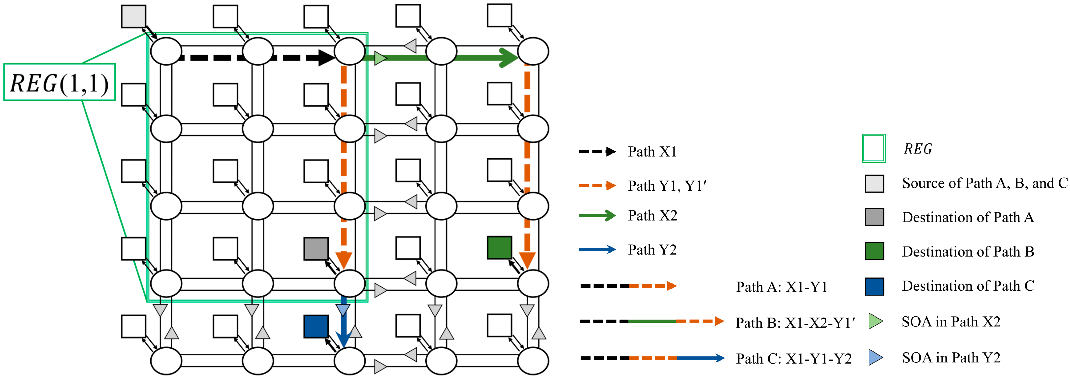
4.2.1. SNR Analysis with Multiple SOAs Using Segmented Regions in Mesh-Based HONoCs

To facilitate the analysis of the SNR change resulting from SOAs and crosstalk, the entire on-chip optical network is partitioned into several sub regions. The criteria for region partitioning are that no sub region should contain any SOA inside and should be surrounded by the SOA-placed links. The sub region is denoted as R E G ( i , j ) where i and j indicate the row and column position, respectively, as shown in Figure 7.
It is apparent that the crosstalk noise introduced at the same R E G with the source node of the optical signal to be routed will be subject to the same number of SOAs as the optical signal, whereas the other crosstalk noises introduced at nearby R E G s to the destination node will be amplified to a lesser degree by the SOAs than by the optical signal under analysis. More specifically, we formulated the SNR of the optical signal path that travels from R E G ( 1 , 1 ) to R E G ( n x , n y ) in Equation (13a) for an SOA-enabled HONoC. For comparison purposes, the SNR for the non-SOA case is derived in Equation (13b).
S N R 1 = 10 log ( P S L R E G ( 1 , 1 ) ( n x , n y ) i N R E G ( 1 , i ) L R E G ( 1 , i + 1 ) ( n x , n y ) G ( i 1 ) + j N R E G ( j , n x ) L R E G ( j + 1 , n x ) ( n x , n y ) G ( n x 1 ) + ( j 1 ) )
S N R 2 = 10 log ( P S L R E G ( 1 , 1 ) ( n x , n y ) i N R E G ( 1 , i ) L R E G ( 1 , i + 1 ) ( n x , n y ) + j N R E G ( j , n x ) L R E G ( j + 1 , n x ) ( n x , n y ) )
i { 1 , ,   n x 1 } , j { 1 , ,   n y }
Here, the total crosstalk noise introduced into the optical signal when it passes through R E G ( i , j ) is represented by N R E G ( i , j ) and the signal power loss that occurs when migrating from R E G ( i 0 , j 0 ) to R E G ( i 1 , j 1 ) is denoted by L R E G ( i 0 , j 0 ) ( i 1 , j 1 ) . Additionally, n x and n y are the number of subregions divided by the SOA-placed links in the X and Y axes, respectively.
In the non-SOA enabled HONoC, the SNR decreases as the routing path length increases as a result of increased signal attenuation and more involved crosstalk noises. In the proposed architecture, the effect of additional crosstalk noise according to the path length increase decreases by the appropriate placement of SOAs to boost the SNR. As shown in Equation (13a), the noise terms decrease by G 0 , G 1 , … and G n x + n 7 2 , respectively. The SNR enhancement becomes more apparent as the number of R E G s increases. Therefore, at the router level, we analysed a path that passes through the greatest number of R E G s and a path inside an R E G .

4.2.2. SNR Analysis of the Longest Path

As the worst-case SNR of the longest path can vary depending on the dominant crosstalk affected by the SOA gain, the SNR values of three representative cases are analysed as follows.
(1)
Case 1: h = 0 , G | L a v g |
S N R 1 L / K [ ( ( G L ) 1 + 2 G L ) ( i = 0 2 m 3 1 ( G L ) i ) ( G L ) ( m 2 ) + ( G L ) ( m 4 ) ]
(2)
Case 2: h = 0 , G > | L a v g |
S N R 1 L / K [ ( ( G L ) 1 + ( G L ) m 1 ) ( i = 0 2 m 3 1 ( G L ) i ) + ( ( G L ) m 1 + 1 ) ( i = 0 m 2 1 ( G L ) 2 i ) ]
(3)
Case 3: h = 2 m 1
S N R 3 L / K [ ( L 1 + 2 L ) ( i = 0 2 m 3 1 L i ) L ( m 2 ) + L ( m 4 ) ]
The case when h = 0 indicates that SOAs are placed on all waveguides, whereas there is no SOA when h = 2 m 1 . When h = 0 , a R E G consists of only one router. As shown in Figure 8a of Case 1, the incoming crosstalk from the nearest router is dominant. In contrast, the crosstalk introduced from the farthest router causes the worst-case SNR in Case 2 as shown in Figure 8b.
As shown in Equation (14a) and (14c), S N R 1 and S N R 3 have an identical form because of the same traffic pattern for the worst-case SNR in the network. If the G L of S N R 1 is replaced by L 1 and if the L of S N R 3 is L 3 , then L 1 is always less than L 3 . Therefore, S N R 1 is always greater than S N R 3 because the insertion loss of Case 1 is smaller than that of Case 3.
In contrast, some crosstalk components have the chance to be amplified more times than the optical signal by SOAs as described in Case 2. In Equation (14b), ( G L ) m 1 represents the worst crosstalk noise due to the SOAs and ( G L ) i indicates the ratio of the number of SOAs that the optical signal passes through to the number of the SOAs that the introduced crosstalk noise passes through. Therefore, if ( G L ) m 1 is larger than ( G L ) i , this implies that the number of SOAs that the crosstalk noise passes through is greater than the number of SOAs that the optical signal passes through. Consequently, S N R 2 severely degrades and eventually can be smaller than S N R 3 as the SOA gain grows.

4.2.3. SNR Analysis inside Regions without SOAs

As previously described, the SNR can be improved when the optical signal passes through multiple SOAs with suitable SOA gain control. However, if the optical signal path forms within a certain R E G , the SNR can degrade compared to a non-SOA HONoC, even if the condition G < | L a v g | is satisfied.
When there is a path that travels along the boundary of R E G , as shown in Figure 9, both the crosstalk noise occurring inside R E G and the optical signal will not pass through any SOA, whereas the crosstalk noise originating from the outside of R E G is amplified by SOAs.
The worst-case SNR of the SOA-integrated HONoC under the corresponding traffic condition and that of the HONoC without SOAs under the same condition can be expressed as follows:
(1)
Case 1: 0 < h < 2 m 1 , G < | L a v g |
S N R 1 L t x + t y 1 / K [ G L ( 2 i = 1 t x L t x + t y 1 i + i = 2 t y L t y i ) + 2 ( i = 1 t x 2 L t x + t y i + i = 1 t y 2 L t y i ) + ( L t y + 1 + L t y + L ) + ( i = 1 t x + t y 2 L t x + t y 2 i ) ]
(2)
Case 2: h = 2 m 1
S N R 2 L t x + t y 1 / K [ L ( 2 i = 1 t x L t x + t y 1 i + i = 2 t y L t y i ) + 2 ( i = 1 t x 2 L t x + t y i + i = 1 t y 2 L t y i ) + ( L t y + 1 + L t y + L ) + ( i = 1 t x + t y 2 L t x + t y 2 i ) ]
Case 1 represents the SOA-integrated HONoC and Case 2 denotes the HONoC without SOAs. In Equation (15a), the first term in the denominator is the crosstalk noise introduced from outside of R E G and amplified by the SOA gain ( G ). Assuming the same optical signal power for both cases, the SNR of the SOA-integrated HONoC is less than that of the HONoC without SOAs. Therefore, if the SOAs are not placed on every link, there is a path along which the SNR decreases.

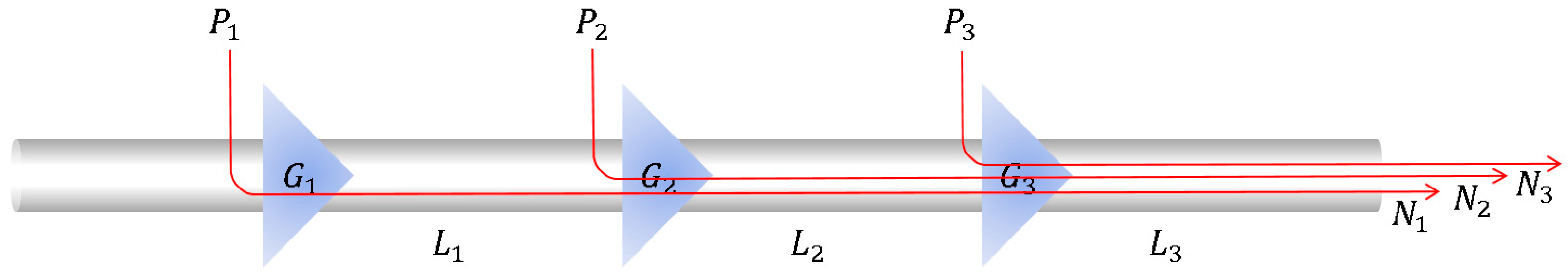
4.3. Minimum SOA Gain and Laser Source Power Allocation

In a conventional mesh-based HONoC, a laser source power is applied considering the insertion loss of the longest path and the receiver sensitivity. However, in the proposed SOA-enabled HONoC, a new analysis of the worst-case insertion loss is required, as the optical signal is amplified whenever it passes through the SOA. If the total SOA gain is larger than the total insertion loss of the overall signal path, the signal power at the destination is greater than that at the source. Therefore, we present the allocation of the laser source power independent of the longest path considering the SOA placement, SOA gain and mesh size.

4.3.1. Minimum SOA Gain Allocation

The SOA gain should be sufficiently large to compensate for the insertion loss between two adjacent SOAs along the signal path. Thus, the laser source power need not be increased even if the network size grows. Overall, the laser source power level is determined by the insertion loss of the longest signal path that does not pass through any SOAs.
As shown in Figure 10, the top-leftmost sub region R E G ( 1 , 1 ) occupies the largest area among the sub regions because uniform placement of SOAs is performed from the top-leftmost corner of the network according to the proposed SOA placement algorithm. Assuming that the reference laser source power level is calculated by considering the longest path formed within R E G ( 1 , 1 ) , we can compute the minimum SOA gain to compensate for the insertion loss without increasing the laser source power.
Once the laser source power is determined by the insertion loss of Path A, the next step is to identify the larger insertion loss between Path B and Path C to compute the minimum SOA gain. Finally, the minimum SOA gain is chosen as the larger value between the insertion loss of Path X2 and that of Path Y2. To summarize, the minimum SOA gain can be expressed as follows:
G m i n = m a x ( L X 2 , L Y 2 ) ,
where L X 2 and L Y 2 denote the insertion loss of Paths X2 and Y2, respectively. Considering mesh size and SOA spacing, we propose the following algorithm to calculate the minimum SOA gain:
Algorithm 2. Calculation for the Minimum SOA Gain
Input: mesh size ( m , n ), SOA spacing ( t x , t y )
Output: minimum SOA gain ( G m i n )
1: n x = ( n 1 ) / t x , n y = ( m 1 ) / t y
2:If n x 2 then
3:   L X 2 = m a x ( L W , E ,   L E , W ) × t x
4:Else
5:   L X 2 = m a x ( L W , E ,   L E , W ) × ( n t x )
6:End if
7:If n y 2 then
8:   L Y 2 = m a x ( L S , N , L N , S ) × t y
9:Else
10:   L Y 2 = m a x ( L S , N , L N , S ) × ( m t y )
11:End if
12: G m i n = m a x ( L X 2 , L Y 2 )
As the optical signal passes through the router in a straight manner, Algorithm 2 checks the paths ( W E ) and ( E W ) in the X-axis and ( S N ) and ( N S ) in the Y-axis, respectively, to find the maximum power loss. Then, L X 2 and L Y 2 are independently calculated for each axis. If n x   2, the maximum hop count is the SOA spacing along the X-axis ( t x ) (lines 2–3). Otherwise, the hop count is the number of routers in the X-axis ( n ) excluding t x (lines 4–6). The same process is performed on the Y-axis (lines 7–11) and the larger insertion loss between L X 2 and L Y 2 is chosen as the minimum SOA gain (line 12).

4.3.2. Minimum Laser Source Power Allocation

When the SOA effectively compensates for the insertion loss along the optical signal path, the worst-case insertion loss depends on h , which is the maximum number of hops along which the optical signal does not pass through any SOAs. If h = 0 , the maximum insertion loss case occurs when the length of the optical signal path is one hop as the optical signal is amplified just once. Otherwise, the worst insertion loss is among the sub-longest paths that are not amplified by the SOA.
When the waveguide crossing loss is –0.12 dB, the insertion loss of the input/output port in the 5   ×   5 Crux router is shown in Table 2. The crux router is the optimized optical router for the insertion loss and the SNR when using X-Y routing [25]. A shown Table 2, the optical router has different insertion loss values depending on the signal flow at the input/output ports. Therefore, the total power loss depends on the routing path even if the number of hops that the optical signal travels along are the same. The worst-case insertion loss according to h considering the input and output port is as follows.
(1)
h = 0 ,   1
P w o r s t _ I L = ( L I n , E +   L W , E j )   o r   ( L I n , N +   L S , E j )
(2)
h = 2
P w o r s t _ I L = ( L I n , E +   L W , N +   L S , E j )
(3)
h 3
P w o r s t _ I L =   ( L I n , E +   L W , N + L S , N × ( h 2 ) +   L S , E j )
Here, the loss values are in dB units. When h = 0 , the worst-case insertion loss is equal to the case of h = 1 , as the SOA exists in all links; however, the SOA gain should be additionally considered when calculating the minimum laser source power. Therefore, the minimum laser source power according to h can be expressed as follows:
P l a s e r _ m i n = { P w o r s t _ I L + P s e n s i t i v i t y P g a i n ,       h = 0 P w o r s t _ I L + P s e n s i t i v i t y ,       h 0
where P w o r s t _ I L is the worst-case insertion loss in the SOA-enabled HONoC, P s e n s i t i v i t y is the minimum optical power required by the photodetector and P g a i n is the SOA gain.

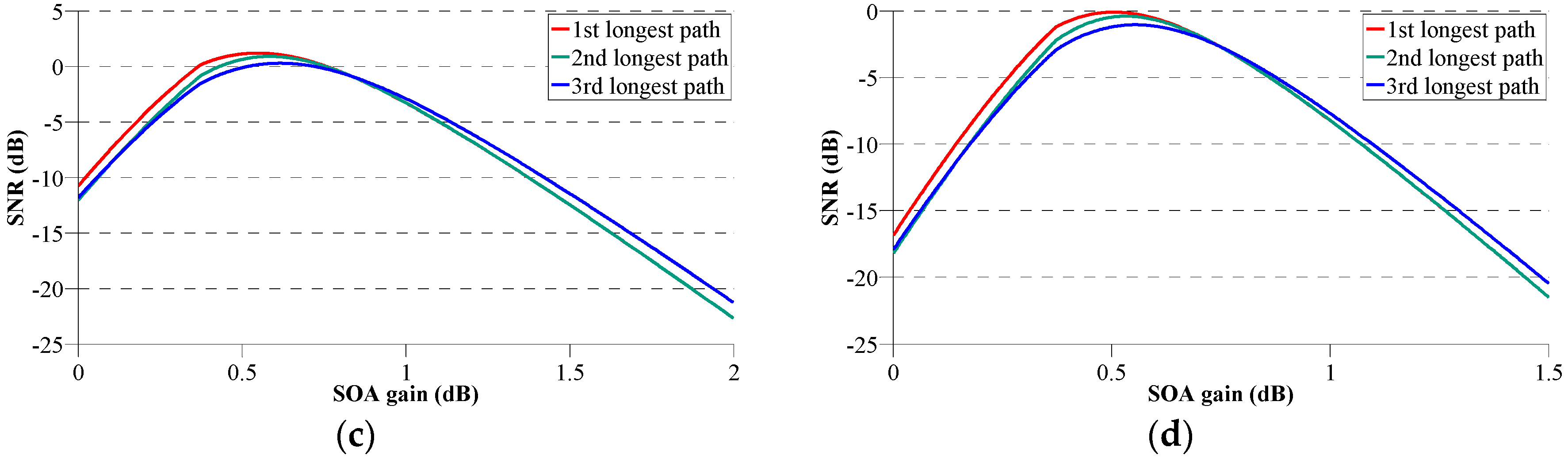
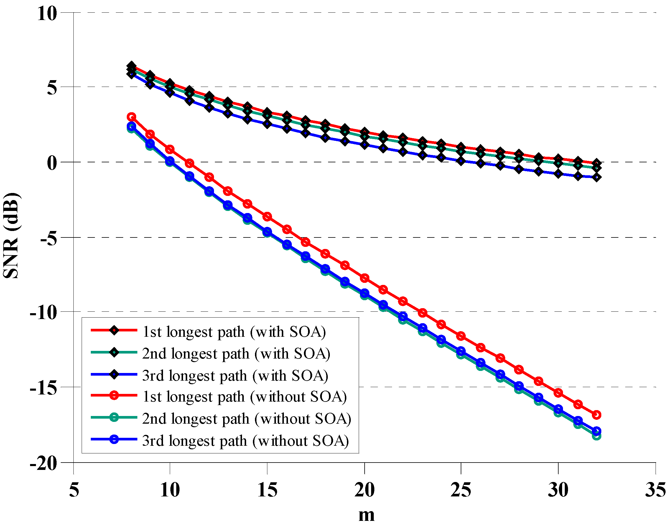
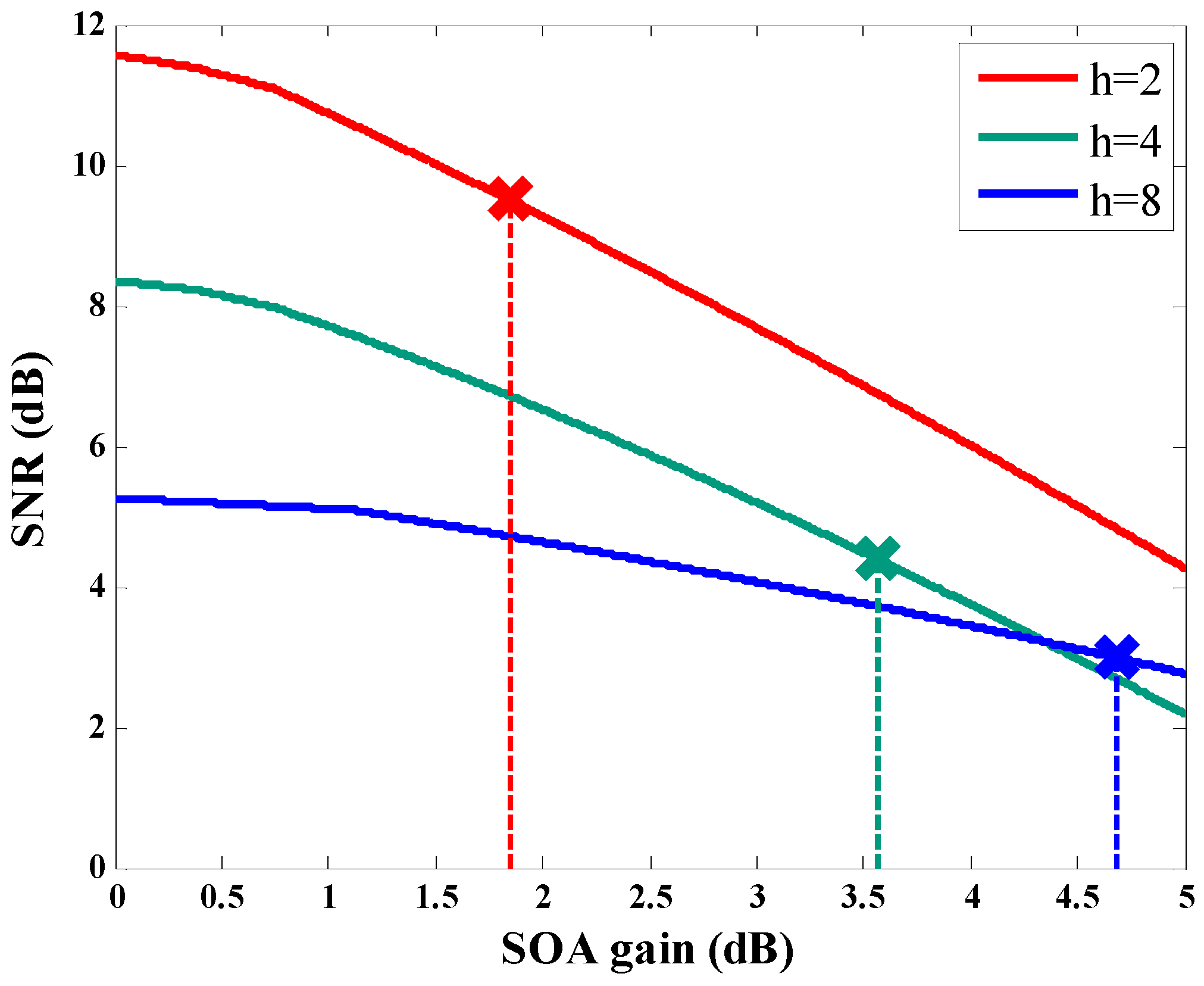
5. Simulation Results
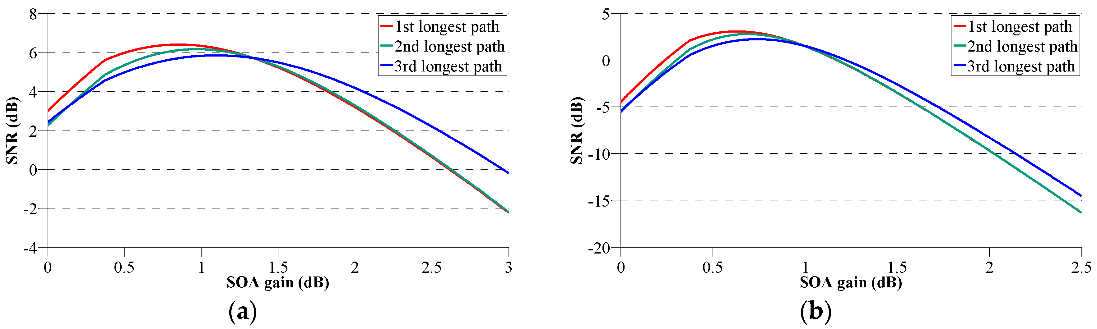
We built up a C-based simulator to evaluate the SNR and the power consumption of the SOA-enabled mesh-based HONoC in comparison with an HONoC without SOAs. The typical values of insertion loss and crosstalk coefficient for system analysis are presented in Table 3. The chip size of 16   ×   16 HONoC is assumed as 1   c m 2 and in other cases, the chip sizes are assumed to be proportional to the number of cores. It is reasonable to suppose that the chip size of the SOA-enabled HONoC is the same as that of the conventional one, as the SOA is small enough to be embedded in a waveguide without widening the space between photonic devices. The traffic patterns are generated using modified BookSim [26] and Crux router is deployed because it is optimized for insertion loss and SNR in the mesh topology.

5.1. SNR Analysis

In the conventional m × n mesh-based HONoC, it is proved formally that the worst-case SNR is among the 1st, 2nd and 3rd longest paths and the best SNR performance is achieved when m = n [19]. For fair comparison, symmetric mesh topologies are chosen for evaluations.
Figure 11 shows worst-case SNR for the 1st, 2nd and 3rd longest paths according to the SOA gain when every link contains an SOA and the network size is 8 × 8 , 16 × 16 , 24 × 24 and 32 × 32 , respectively. When the SOA gain is 0 dB, the SNR values are the same as that for non-SOA HONoCs. The SNR gradually improves as the SOA gain increases, whereas it decreases at a certain threshold of the SOA gain. Furthermore, the SNR decreases further than that of the conventional HONoC without SOAs if the SOA gain increases even more.
Figure 12 shows the worst-case SNR of the SOA-enabled HONoC and that of the conventional HONoC according to the mesh size in an m × m mesh. When the network size is larger than 12 × 12 , the noise power exceeds the signal power in the mesh-based HONoC. In addition, the SNR decreases drastically as the network size increases. However, in our proposed architecture, the SNR of the 1st, 2nd and 3rd longest paths are 1.19 dB, 0.89 dB and 0.28 dB when the network size is 24 × 24 . When the network size is 32 × 32 , the worst-case SNR is –1.05 dB and the SNR degradation is not large even if the network size is further increased. As the worst-case SNR determines the feasibility and the scalability of the HONoC, the proposed architecture shows a great advantage over the conventional HONoC architecture.
Figure 13 shows the SNR improvement in an average basis for the 1st, 2nd and 3rd longest paths with respect to the maximum hop count without SOAs, h . The number of SOAs is proportional to the mesh size and is inversely proportional to h . When the mesh size is smaller and h is larger, the amplification of the optical signal is relatively small. On the contrary, the amplification of the introduced crosstalk noise occurs frequently when the mesh size is larger and h is smaller. Therefore, the SNR improvement is closely related to the mesh size as well as h , which determines the number of SOAs in the optical signal path. When the SOA placement is performed according to the optimal h , the SNR is improved by 4.26 dB, 8.91 dB, 13.69 dB and 18.65 dB when the network size is 8 × 8 , 16 × 16 , 24 × 24 and 32 × 32 , respectively. Therefore, the degradation of the worst-case SNR in the large-scale HONoC can be mitigated through the placement of SOAs.
Figure 14 shows the worst-case SNR reduction of the non-SOA region surrounded by the SOA-placed links, in accordance with the SOA gain. As previously analysed in Section 4.2.2, there is a path in which the SNR decreases due to the several amplified crosstalk noises, compared to the equivalent optical signal power if the SOAs are not placed on all links ( h 0 ).
When h becomes smaller, the SNR of the longest path traveling along the boundary decreases more as the SOA gain increases. This result denotes that the shorter path length is more affected by the amplified crosstalk noise. However, as marked X in Figure 14, the appropriate SOA gain for the worst-case SNR on the whole network differs depending on h . The SNR losses at the mark X are 2.06 dB, 3.96 dB and 2.26 dB when h = 2 , h = 4 and h = 8 , respectively. The SNR reduction is the smallest when h = 2 ; however, there are more paths in which such SNR degradation occurs in the network because the SOA spacing is narrower than in other cases. In other words, it means that SNR degradation may occur when SOA spacing is narrow but it does not occur in the same path when SOA spacing is wide. Therefore, h = 8 can be the best case considering both the magnitude of SNR reduction and the probability that these SNR-reduced paths will occur.

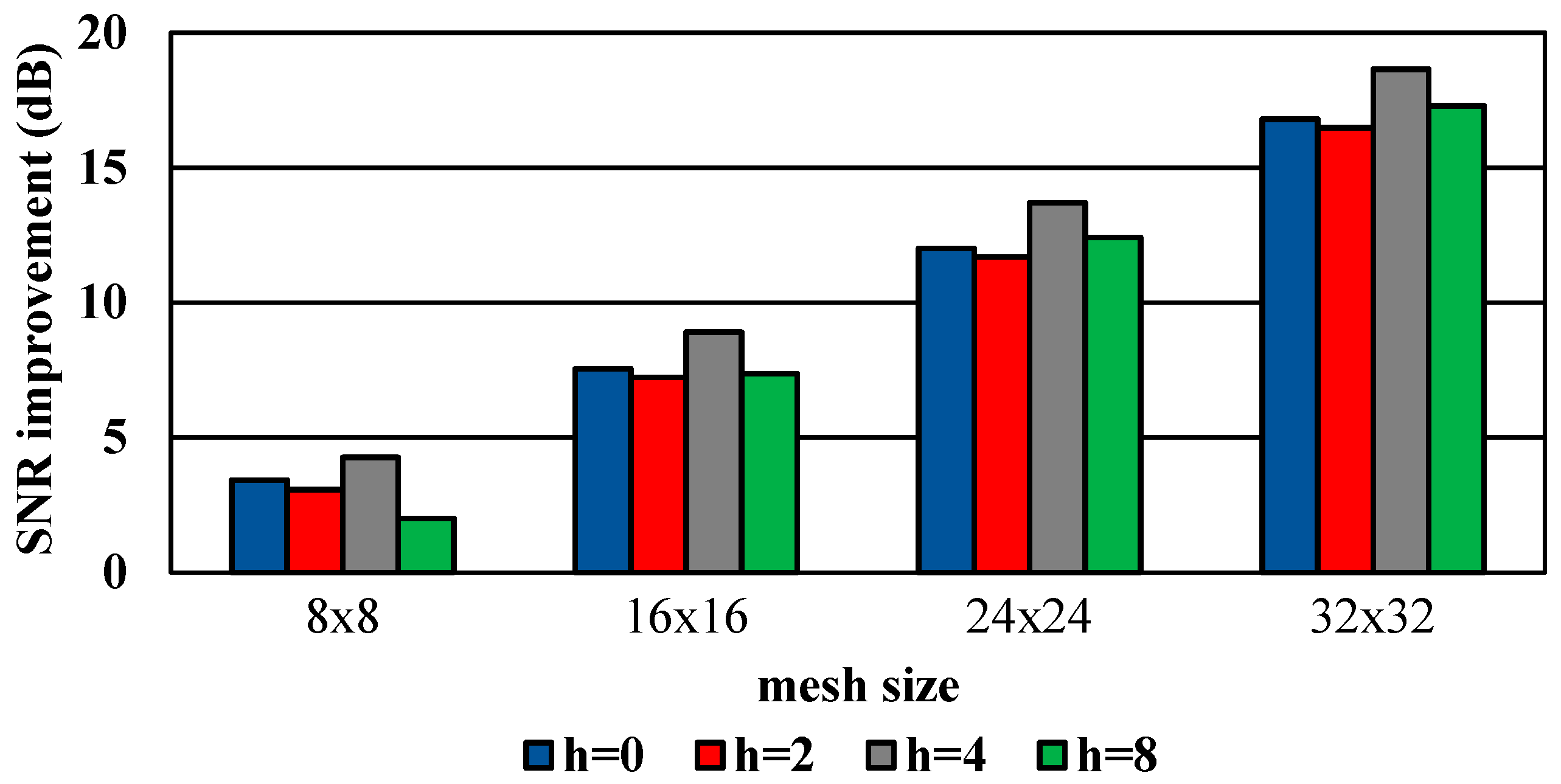
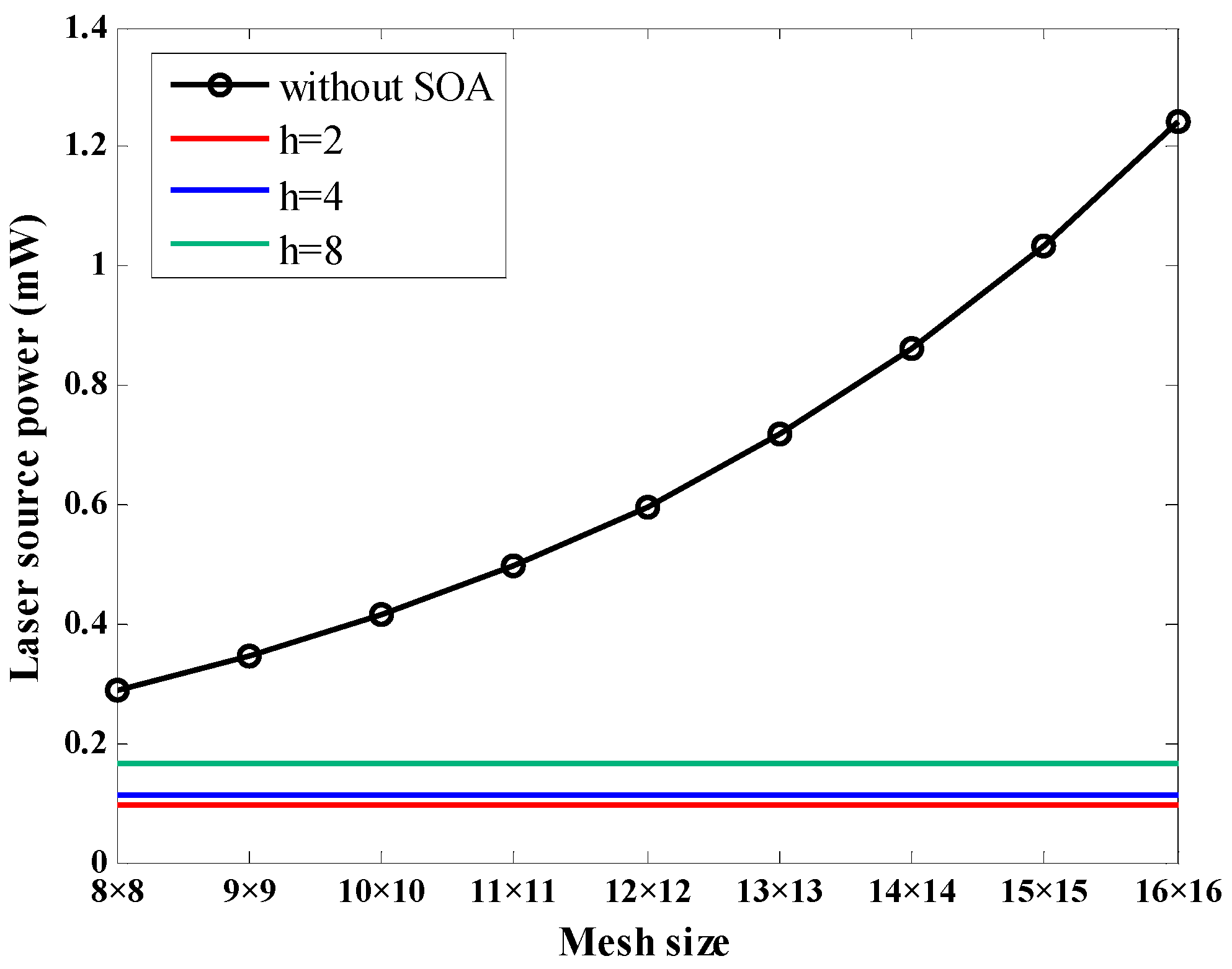
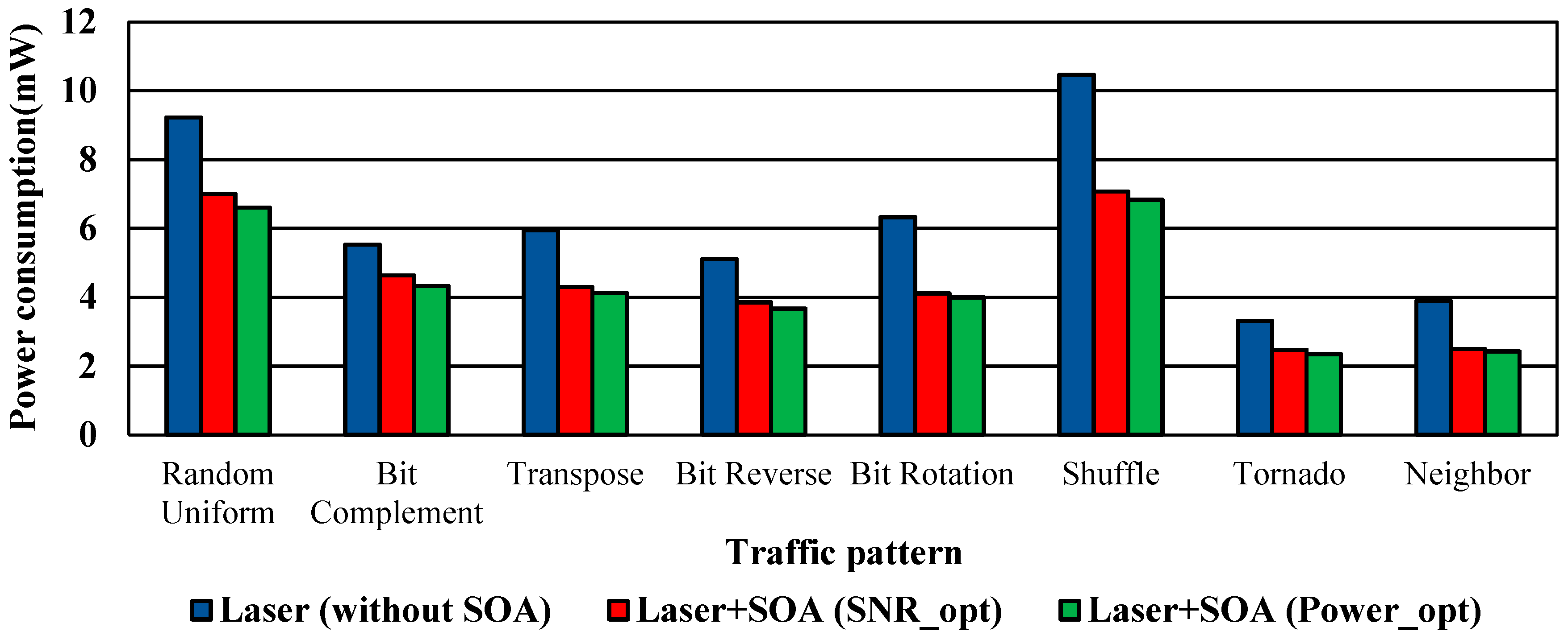
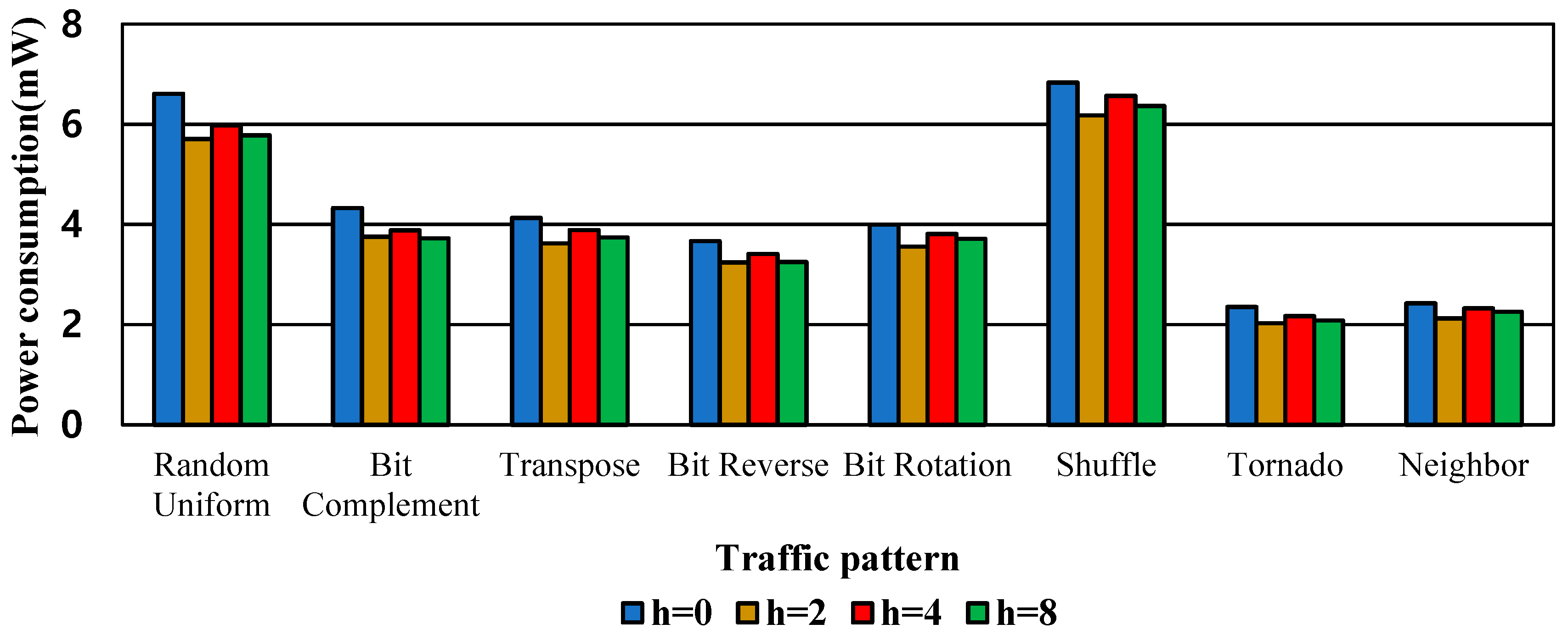
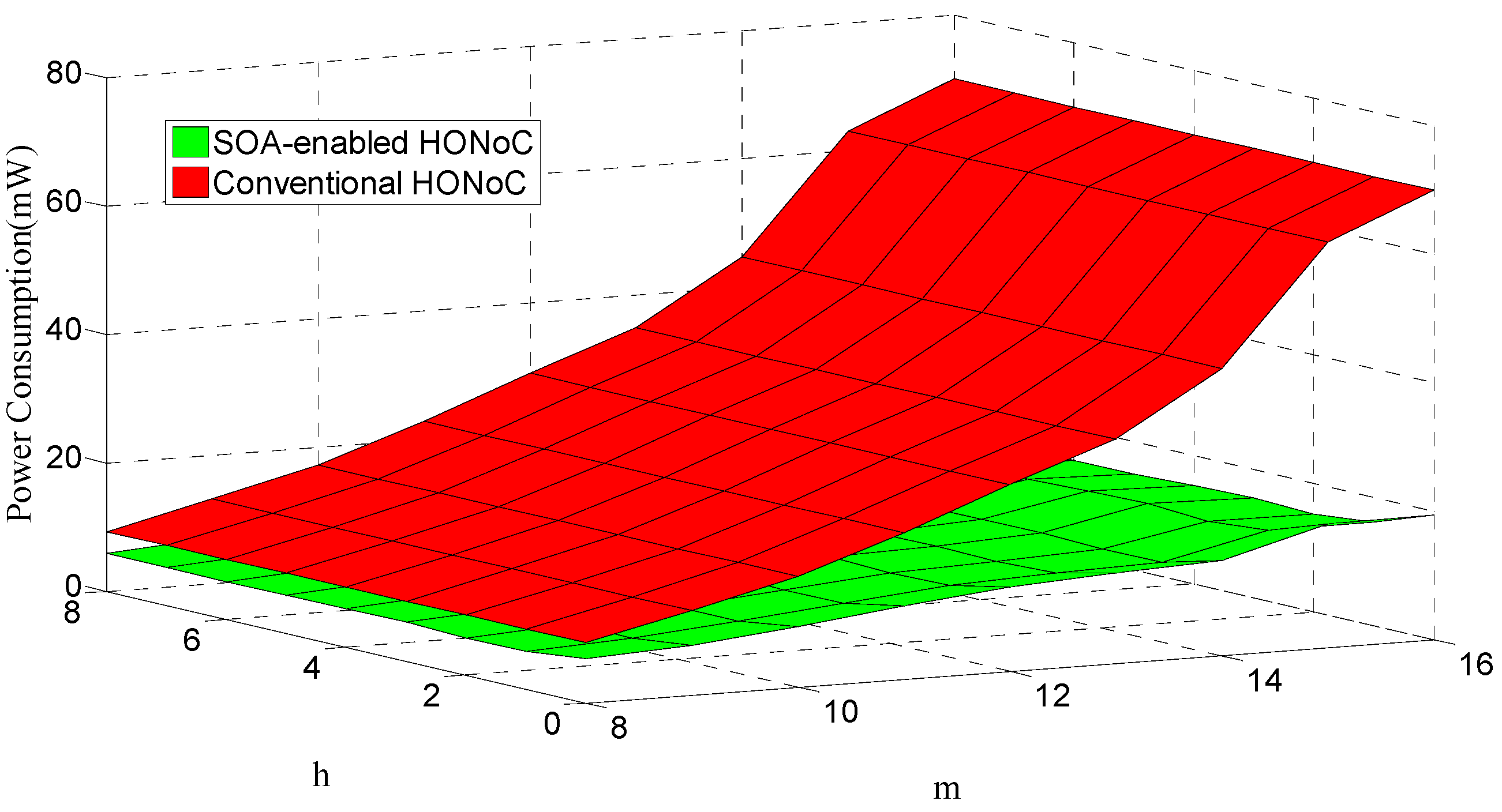
5.2. Power Consumption

Figure 15 shows the laser source power considering the mesh size, the placement of the SOA and the worst-case insertion loss. We assume that the efficiency of the laser source power is 20% [29]. If there is no SOA, the laser source power increases sharply as the mesh size increases. In the SOA-enabled HONoC, however, the laser source power is independent of the mesh size. Although additional power consumption due to the SOAs will be inevitable, it is expected to be a comparable trade-off owing to the laser source power savings that will be realized by incorporating this work.
With common traffic patterns for NoCs, the simulation results in terms of power consumption in the conventional HONoC and the SOA-enabled HONoC are illustrated in Figure 16. We assume that the mesh size is 8   × 8 and SOAs are placed on every waveguide where the laser source power is the smallest. According to the previous studies, the power consumption of MR activation has been reported as 50 μ W [30]. Simulation was performed on the HONoC without SOAs and the SOA-enabled HONoCs optimized for SNR and power consumption, respectively. Power consumption is reduced by 16.26–35.86% when focusing on the SNR and by 21.81–37.68% when focusing on the total power consumption. There is a slight difference in power consumption between when optimizing for SNR and when optimizing for power consumption.
Figure 17 shows the total power consumption according to the maximum hop count of possible paths without SOAs ( h ) and different traffic patterns when network size is 8   × 8. When h = 0 , the laser source power can be reduced by the SOA gain; however, the efficiency of the SOA gain is low and the number of SOAs is the most. If h 0 , the number of SOAs in the network is reduced as h increases; however, the laser source power and single SOA power consumption increase.
When h = 4 , the number of SOAs is twice as high as when h = 8 and the power consumption increases. Furthermore, in the case of h = 2 , the number of SOAs is three times higher than when h = 8 ; however, the power consumption is reduced slightly or similar. Therefore, the total power consumption in relation to h is hard to predict because it is determined by the total sum of the power consumption per unit SOA, the number of SOAs in the network and the laser source power. Simulation results show that the power consumption is the largest when h = 0 ; therefore, placing SOAs on all links is inefficient in terms of power consumption. Contrarily, the minimum power consumption is achieved when h = 2 and the overall power consumption of the SOA-enabled HONoC is reduced by 32.17–45.49%, compared to the conventional HONoC.
Figure 18 shows the comparison of power consumption between the SOA-enabled HONoC and the conventional HONoC according to the mesh size and the hop count between SOAs in a random uniform pattern. The increase in the power consumption in the proposed HONoC is relatively low compared to that in the conventional HONoC because the insertion loss is independent of the longest path. As a result, the power saving realized by the proposed approach becomes prominent as the mesh size grows.

6. Conclusions

We proposed the SOA-enabled HONoC architecture to reduce the total power consumption and mitigate SNR degradation, considering network size scalability without increasing laser source output power. An SOA placement algorithm was developed for efficient laser source power reduction and SNR enhancement. We suggested the worst-crosstalk noise model and presented the attuning method for optimal SOA gain with respect to power consumption and SNR, respectively. We constructed a C-based simulator to evaluate the SOA-enabled HONoC with an associated SOA placement algorithm. Simulation results showed that the worst-case SNRs for the 1st, 2nd and 3rd longest paths are improved by an average of 4.26 dB and power consumption is reduced by 32.17% to 45.49% under various traffic patterns in the 8 × 8 network. The performance gaps regarding various SOA spacings were not significant; on the other hand, the improvement achieved in both SNR and power consumption was increased in proportion to the mesh size. Therefore, the proposed SOA-enabled HONoC can be a scalable solution to cope with the performance degradation problem of large-scale HONoCs.

Author Contributions

Formal analysis, J.Y.J.; Investigation, C.-L.L.; Methodology, M.S.K.; Validation, J.Y.J.; Writing—original draft, J.Y.J.; Writing—review & editing, T.H.H.

Funding

This research was funded by the Basic Science Research Program through the National Research Foundation of Korea under Grant NRF-2018R1D1A1B07043585 and by the MOTIE (Ministry of Trade, Industry & Energy) (10080594) and KSRC (Korea Semiconductor Research Consortium) support program for the development of the future semiconductor device.

Conflicts of Interest

The authors declare no conflict of interest.

References

  1. Vantrease, D.; Schreiber, R.; Monchiero, M.; McLaren, M.; Jouppi, N.P.; Fiorentino, M.; Davis, A.; Binkert, N.; Beausoleil, R.G.; Ahn, J.H. Corona: System implications of emerging nanophotonic technology. In Proceedings of the IEEE/ACM International Symposium on Computer Architecture (ISCA), Beijing, China, 21–25 June 2008. [Google Scholar]
  2. International Technology Roadmap for Semiconductors. Available online: http://www.itrs2.net (accessed on 27 September 2018).
  3. Shacham, A.; Bergman, K.; Carloni, L.P. Photonics Networks-on-Chip for Future Generations of Chip Multiprocessors. IEEE Trans. Comput. 2008, 57, 1246–1260. [Google Scholar] [CrossRef]
  4. Mo, K.H.; Ye, Y.; Wu, X.; Zhang, W.; Liu, W.; Xu, J. A Hierarchical Hybrid Optical-Electronic Network-on-Chip. In Proceedings of the 2010 IEEE Computer Society Annual Symposium on VLSI, Lixouri, Kefalonia, Greece, 5–7 July 2010. [Google Scholar]
  5. Gu, H.; Xu, J.; Wang, Z. A novel optical mesh network-on-chip for gigascale systems-on-chip. In Proceedings of the 2008 IEEE Asia Pacific Conference on Circuits and Systems, Macao, China, 30 November–3 December 2008. [Google Scholar]
  6. Lee, J.; Kim, Y.; Li, C.; Han, T. A shortest path adaptive routing technique for minimizing path collision in hybrid optical network-on-chip. J. Syst. Arch. 2013, 59, 1334–1347. [Google Scholar] [CrossRef]
  7. Lan, F.; Wu, R.; Zhang, C.; Pan, Y.; Cheng, K.-T.T. DLPS: Dynamic laser power scaling for optical Network-on-Chip. In Proceedings of the 2017 22nd Asia and South Pacific Design Automation Conference (ASP-DAC), Chiba, Japan, 16–19 January 2017. [Google Scholar]
  8. Xie, Y.; Nikdast, M.; Xu, J.; Zhang, W.; Li, Q.; Wu, X.; Ye, Y.; Wang, X.; Liu, W. Crosstalk noise and bit error rate analysis for optical network-on-chip. In Proceedings of the ACM/IEEE Design Automation Conference, Anaheim, CA, USA, 13–18 June 2010. [Google Scholar]
  9. Xiao, S.; Khan, M.H.; Shen, H.; Qi, M. Multiple-channel silicon micro-resonator bad filters for WDM applications. Opt. Express 2007, 15, 7489–7498. [Google Scholar] [CrossRef] [PubMed]
  10. Eid, N.; Boeck, R.; Jayatilleka, H.; Chrostowski, L.; Shi, W.; Jaeger, N.A.F. A silicon-on-insulator microring resonator filter with bent contradirectional couplers. In Proceedings of the 2016 IEEE Photonics Conference (IPC), Waikoloa, HI, USA, 2–6 October 2016. [Google Scholar]
  11. Fusella, E.; Cilardo, A. Lighting Up On-Chip Communications with Photonics: Design Tradeoffs for Optical NoC Architectures. IEEE Circuits Syst. Mag. 2016, 16, 4–14. [Google Scholar] [CrossRef]
  12. Poon, A.W.; Xu, F.; Luo, X. Cascaded active silicon microresonator array cross-connect circuits for WDM networks-on-chip. In Proceedings of the SPIE—The International Society for Optical Engineering, San Jose, CA, USA, 13 February 2008. [Google Scholar]
  13. Ding, W.; Tang, D.; Liu, Y.; Chen, L.; Sun, X. Compact and low crosstalk waveguide crossing using impedance matched metamaterial. Appl. Phys. Lett. 2010, 96, 111114. [Google Scholar] [CrossRef]
  14. Biberman, A.; Preston, K.; Hendry, G.; Sherwood-Droz, N.; Chan, J.; Levy, J.S.; Lipson, M.; Bergman, K. Photonic network-on-chip architectures using multilayer deposited silicon materials for high-performance chip multiprocessors. ACM J. Emerg. Technol. Comput. Syst. 2011, 7, 7. [Google Scholar] [CrossRef]
  15. Dong, P.; Qian, W.; Liao, S.; Liang, H.; Kung, C.-C.; Feng, N.-N.; Shafiiha, R.; Fong, J.; Feng, D.; Krishnamoorthy, A.V.; et al. Low Loss Silicon Waveguides for Application of Optical Interconnects. In Proceedings of the IEEE Photonics Society Summer Topicals 2010, Playa del Carmen, Mexico, 19–21 July 2010. [Google Scholar]
  16. Lee, B.G.; Biberman, A.; Dong, P.; Lipson, M.; Bergman, K. All-Optical Comb Switch for Multiwavelength Message Routing in Silicon Photonic Networks. IEEE Photonics Technol. Lett. 2008, 20, 767–769. [Google Scholar] [CrossRef]
  17. Sanchis, P.; Galan, J.V.; Brimont, A.; Griol, A.; Marti, J.; Piqueras, M.A.; Perdigues, J.M. Low-crosstalk in silicon-on-insulator waveguide crossings with optimized-angle. In Proceedings of the 2007 4th IEEE International Conference on Group IV Photonics, Tokyo, Japan, 19–21 September 2007. [Google Scholar]
  18. Chen, H.; Poon, A.W. Low-Loss Multimode-Interference-Based Crossings for Silicon Wire Waveguides. IEEE Photonics Technol. Lett. 2006, 18, 2260–2262. [Google Scholar] [CrossRef]
  19. Xie, Y.; Nikdast, M.; Xu, J.; Wu, X.; Zhang, W.; Ye, Y.; Wang, X.; Wang, Z.; Liu, W. Formal Worst-Case Analysis of Crosstalk Noise in Mesh-Based Optical Networks-on-Chip. IEEE Trans. Very Large Scale Integr. Syst. 2013, 21, 1823–1836. [Google Scholar] [CrossRef]
  20. Nikdast, M.; Xu, J.; Wu, X.; Zhang, W.; Ye, Y.; Wang, X.; Wang, Z.; Wang, Z. Systematic Analysis of Crosstalk Noise in Folded-Torus-Based Optical Networks-on-Chip. IEEE Trans. Comput. Aided Des. Integr. Circuits Syst. 2014, 33, 437–450. [Google Scholar] [CrossRef]
  21. Duong, L.H.K.; Nikdast, M.; Xu, J.; Wang, Z.; Thonnart, Y.; Beux, S.L.; Yang, P.; Wu, X.; Wang, Z. Coherent crosstalk noise analyses in ring-based optical interconnects. In Proceedings of the 2015 Design, Automation and Test in Europe Conference and Exhibition (DATE), Grenoble, France, 9–13 March 2015. [Google Scholar]
  22. Nikdast, M.; Xu, J.; Duong, L.H.K.; Wu, X.; Wang, Z.; Wang, X.; Wang, Z. Fat-Tree-Based Optical Interconnection Networks Under Crosstalk Noise Constraint. IEEE Trans. Very Large Scale Integr. Syst. 2014, 23, 156–169. [Google Scholar] [CrossRef]
  23. Rostami, A.; Baghban, H.; Maram, R. Nanostructure Semiconductor Optical Amplifiers, 1st ed.; Springer: Berlin, Germany, 2011; Available online: https://books.google.com.hk/books?hl=en&lr=&id=xN0PXG_38SIC&oi=fnd&pg=PR3&dq=Nanostructure+Semiconductor+Optical+Amplifiers&ots=A-G24LLZxf&sig=QA-Sb2u1vHjRxW_K80vxRLDUB4E&redir_esc=y#v=onepage&q=Nanostructure%20Semiconductor%20Optical%20Amplifiers&f=false (accessed on 16 September 2018).
  24. Thakkar, I.G.; Chittamuru, S.V.R.; Pasricha, S. Run-time laser power management in photonic NoCs with on-chip semiconductor optical amplifiers. In Proceedings of the 2016 Tenth IEEE/ACM International Symposium on Networks-on-Chip, Nara, Japan, 31 August–2 September 2016. [Google Scholar]
  25. Ye, Y.; Wu, X.; Xu, J.; Zhang, W.; Nikdast, M.; Wang, X. Holistic comparison of optical routers for chip multiprocessors. In Proceedings of the IEEE 2012 International Conference on Anti-Counterfeiting, Security and Identification (ASID), Taipei, Taiwan, 24–26 August 2012. [Google Scholar]
  26. Jiang, N.; Becker, D.U.; Michelogiannakis, G.; Balfour, J.; Towles, B.; Shaw, D.E.; Kim, J.; Dally, W.J. A detailed and flexible cycle-accurate Network-on-Chip simulator. In Proceedings of the 2013 IEEE International Symposium on Performance Analysis of Systems and Software (ISPASS), Austin, TX, USA, 21–23 April 2013. [Google Scholar]
  27. Bogaerts, W.; Dumon, P.; Thourhout, D.V.; Baets, R. Low-loss, low-cross-talk crossings for silicon-on-insulator nanophotonic waveguides. Opt. Lett. 2007, 32, 2801–2803. [Google Scholar] [CrossRef] [PubMed]
  28. Chan, J.; Hendry, G.; Bergman, K.; Carloni, L.P. Physical-Layer Modeling and System-Level Design of Chip-Scale Photonic Interconnection Networks. IEEE Trans. Comput. Aided Des. Integr. Circuits Syst. 2011, 30, 1507–1520. [Google Scholar] [CrossRef]
  29. Maulini, R.; Lyakh, A.; Tsekoun, A.; Patel, C.K.N. λ~7.1 μm quantum cascade lasers with 19% wall-plug efficiency at room temperature. Opt. Express 2011, 19, 17203–17211. [Google Scholar] [CrossRef] [PubMed]
  30. Joshi, A.; Batten, C.; Kwon, Y.-J.; Beamer, S.; Shamim, I.; Asanovic, K.; Stojanovic, V. Silicon-photonic clos networks for global on-chip communication. In Proceedings of the 2009 3rd ACM/IEEE International Symposium on Networks-on-Chip, San Diego, CA, USA, 10–13 May 2009. [Google Scholar]
Figure 1. Two major insertion losses in optical network-on-chip (ONoC): (a) Microring (MR) drop loss; and (b) waveguide crossing loss.
Applsci 09 01251 g001
Figure 2. Semiconductor optical amplifier (SOA)-enabled HONoC architecture.
Applsci 09 01251 g002
Figure 3. General optical router model.
Applsci 09 01251 g003
Figure 4. Overall flow of the proposed design methodology.
Applsci 09 01251 g004
Figure 5. Example of cumulated crosstalk noise according to the SOA placement.
Applsci 09 01251 g005
Figure 6. Example of crosstalk noise paths whose magnitude order varies depending on SOA gains.
Applsci 09 01251 g006
Figure 7. Non-SOA sub regions ( R E G ) according to the SOA placement algorithm.
Applsci 09 01251 g007
Figure 8. Worst-case SNR of the longest path in accordance with the SOA gain: (a) h = 0 , G | L a v g | ; and (b) h = 0 , G > | L a v g | .
Applsci 09 01251 g008
Figure 9. Worst-case signal to noise ratio (SNR) of the non-SOA region surrounded by SOA-placed links.
Applsci 09 01251 g009
Figure 10. Example of determining the minimum SOA gain considering traffic paths across the top-leftmost non-SOA region.
Applsci 09 01251 g010
Figure 11. Worst-case SNR for SOA-enabled HONoC according to the SOA gain for different network sizes: (a) 8 × 8 ; (b) 16 × 16 ; (c) 24 × 24 ; and (d) 32 × 32 .
Applsci 09 01251 g011aApplsci 09 01251 g011b
Figure 12. SNR comparison for the 1st, 2nd and 3rd longest paths between SOA-enabled HONoC and conventional HONoC (without SOAs) in accordance with the mesh size.
Applsci 09 01251 g012
Figure 13. SNR improvement in an average basis for the 1st, 2nd and 3rd longest paths of the SOA-enabled HONoC according to different h and network sizes.
Applsci 09 01251 g013
Figure 14. SNR reduction in the region surrounded by the SOA-placed links. X indicates the appropriate SOA gain for the worst-case SNR.
Applsci 09 01251 g014
Figure 15. Laser source power comparison between a conventional HONoC (without SOA) and SOA-enabled HONoC.
Applsci 09 01251 g015
Figure 16. Power consumption comparison between a conventional HONoC (without SOA) and SOA-enabled HONoC optimized for SNR and power consumption, respectively, for various traffic patterns.
Applsci 09 01251 g016
Figure 17. Power consumption of an SOA-enabled HONoC according to the SOA spacing for various traffic patterns.
Applsci 09 01251 g017
Figure 18. Power consumption comparison between a conventional HONoC (without SOA) and SOA-enabled HONoC in terms of mesh size and maximum hop count without SOAs.
Applsci 09 01251 g018
Table 1. Definitions and values of SOA parameters.
ParameterDefinitionValue
Γ Light confinement factor 0.4
  a 1 Constant 6.7 × 10 16   cm 2
n 0 Transparency carrier concentration 1.2 × 10 18   cm 3
L Length of the SOA active region 10   μ m
I 0 Threshold input current 5   μ A
α Loss in the SOA active region 10   cm 1
Δ λ SOA gain linewidth 95   nm
Table 2. Loss value in 5 × 5 Crux router.
LossValue (dB)LossValue (dB)
L I n , W 0.50 L E , W 0.38
L I n , E 0.88 L E , N 0.50
L I n , N 0.88 L E , S 1.00
L I n , S 0.63 L E , E j 0.63
L W , E 0.38 L N , S 0.38
L W , N 1.00 L N , E j 0.50
L W , S 0.50 L S , N 0.38
L W , E j 0.88 L S , E j 0.88
Table 3. Loss and crosstalk coefficient values.
ParameterValueReference
Waveguide crossing loss–0.12 dB[12]
Propagation loss per cm–0.274 dB/cm[15]
Power loss of CSE in OFF state–0.04 dB[13]
Power loss of CSE in ON state–0.5 dB[9]
Power loss of PSE in OFF state–0.005 dB[9]
Power loss of PSE in ON state–0.5 dB[9]
Crossing crosstalk coefficient–45 dB[27]
Crosstalk coefficient of PSE in OFF state–20 dB[28]
Crosstalk coefficient of PSE in ON state–25 dB[28]

