Article

Enhanced Device Performance of GaInN-Based Green Light-Emitting Diode with Sputtered AlN Buffer Layer

1
Faculty of Science and Technology, Meijo University, Nagoya 468-8502, Japan
2
Akasaki Research Center, Nagoya University, Nagoya 464-8603, Japan
*
Author to whom correspondence should be addressed.
Appl. Sci. 2019, 9(4), 788; https://doi.org/10.3390/app9040788
Submission received: 26 December 2018 / Revised: 15 February 2019 / Accepted: 19 February 2019 / Published: 23 February 2019
(This article belongs to the Special Issue Internal Quantum Efficiency of III-Nitride Light-Emitting Diodes)

Abstract

:
In this study, we compared the device performance of GaInN-based green LEDs grown on c-plane sapphire substrates with a conventional low temperature GaN buffer layer to those with a sputtered-AlN buffer layer. The light output power and leakage current characteristics were significantly improved by just replacing the buffer layer with a sputtered-AlN layer. To understand the origin of the improvement in performance, the electrical and optical properties were compared by means of electro-reflectance spectroscopy, I–V curves, electroluminescence spectra, L–I curves, and internal quantum efficiencies. From the analysis of the results, we concluded that the improvement is mainly due to the mitigation of strain and reduction of the piezoelectric field in the multiple quantum wells active region.

1. Introduction

Recently, technological progress in III-nitride based wide bandgap semiconductors has been greatly encouraged because of a continuous demand for energy saving, long lifetime, and environmentally friendly devices [1,2,3]. Since the bandgap of GaInN ternary alloys covers a broad spectral range, from visible to ultra-violet, these materials are suitable for optoelectronic devices such as light-emitting diodes (LEDs), laser diodes, solar-cells, and photo-detectors (PDs) [4,5,6,7]. III-nitride based semiconductors are typically grown on sapphire substrates by using metal-organic chemical vapor deposition (MOCVD) because homo-epitaxial substrates are still expensive due to a difficulty in mass production. However, the direct growth of a GaN film on a sapphire substrate leads to very poor crystal quality due to a large difference in the lattice constant and thermal expansion coefficients of the GaN film and the sapphire substrate. This problem was overcome by H. Amano et al., who were the first to demonstrate that crystal quality and surface morphology can be remarkably improved by the introduction of a thin buffer layer [1,8].
Nowadays, III-nitride based LEDs are commercialized for use in highly-efficient solid-state lighting sources. In particular, an external quantum efficiency (EQE) of more than 80% has been reported for blue LEDs [9], whereas the EQE of green LEDs still remains around 30%~40%. That is, the EQE of GaInN-based LEDs drastically decreases as the emission wavelength increases, which is typically known as the “green-gap” problem [10,11]. Several factors are considered to be the origin of the green-gap, including degradation of crystal quality [12], increase of stress [13], alloy fluctuation [14], and the quantum confined stark effect (QCSE) [15]. All of these are fundamentally related to an increase in the indium composition in the active region. One possible solution to overcome the green-gap could be strain engineering that employs a strain compensation/relaxation layer, e.g., superlattice layers (SLs), an AlGaN interlayer, a GaInN underlayer, and graded indium composition across multiple quantum wells (MQWs) in the active region [16,17,18,19].
Recently, we reported the improved photoluminescence (PL) efficiency in a GaInN-based green LED by simply replacing a conventional low temperature GaN buffer layer with a sputtered-AlN buffer layer [20]. In spite of the significant improvement in PL efficiency, the optical and electrical properties under electrical injection were not deeply investigated and the physical mechanism behind the observed improvement is not yet fully understood.
In this study, we compare GaInN-based green LEDs grown on c-plane sapphire substrates with either a conventional low temperature GaN buffer layer or a sputtered-AlN buffer layer. The electrical and optical properties of both LEDs were compared by means of electro-reflectance (ER) spectroscopy, their current–voltage characteristics (I–V curve), electroluminescence (EL), light output power–current characteristics (L–I curve), and internal quantum efficiency-current characteristics (IQE–I curve) to understand the underlying physical mechanisms of the differences in their behavior.

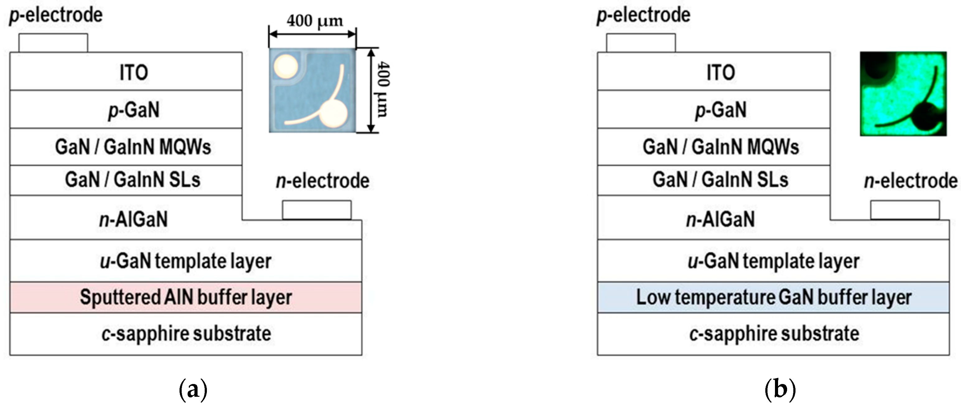
2. Materials and Methods

Schematic illustrations of the LED structure are shown in Figure 1a,b. All samples were grown on c-plane flat sapphire substrates (FSS) with either a sputtered-AlN buffer layer or a conventional low temperature GaN buffer layer. For deposition of the sputtered-AlN buffer layer (Figure 1a), a sintered AlN target was placed ~85 mm from the substrate. After the chamber was evacuated to <5.5 × 10⁻⁵ Pa, an Ar-N2 gas mixture was introduced as the sputtering gas. By controlling the time at 450 W of RF power, a 20-nm thick sputtered-AlN layer was deposited on the FSS at 600 °C. By contrast, for deposition of the low temperature GaN buffer layer (Figure 1b), a 30 nm thick GaN buffer layer was grown on FSS in MOCVD at 470 °C. The epitaxial structure of the green LEDs are identical to each other except for the buffer layer, and was composed of a 4 μm thick u-GaN template layer grown at 1050 °C, a Si-doped n-Al0.02Ga0.98N layer, 10 pairs of Ga0.93In0.07N/GaN (3 nm/3 nm) SLs, and the MQWs consisting of five pairs of 3 nm thick Ga0.77In0.23N QWs sandwiched by 10 nm thick GaN barriers. On top of the MQWs, a Mg-doped p-GaN layer was grown. The indium composition in the MQWs was estimated by X-ray diffraction of both samples. Although we run these samples separately, significant differences cannot be observed in terms of epi-layer thickness and alloy composition between samples.
The chip size was 400 × 400 μm with a conventional lateral electrode structure as shown in the inset of Figure 1. The chip was mounted on a STEM-type metal package without epoxy molding for measuring electrical and optical properties. Hereafter, we refer to green the LEDs grown on a sputtered-AlN buffer layer in Figure 1a, as LED A, and the green LEDs grown on a conventional low temperature GaN buffer layer in Figure 1b, as LED B.
The I–V and capacitance–voltage (C–V) characteristics were measured using an Agilent semiconductor parameter analyzer and an Agilent impedance analyzer, respectively. The C–V characteristics were measured at a fixed modulation frequency of 1 MHz with an amplitude of 10 mV under a reverse bias range. The optical properties including light output power and spectrum were measured by a Si photo-diode and a spectrometer under the pulsed-current driving condition (pulse period = 100 µs and duty cycle = 1%) in order to avoid self-heating, respectively.

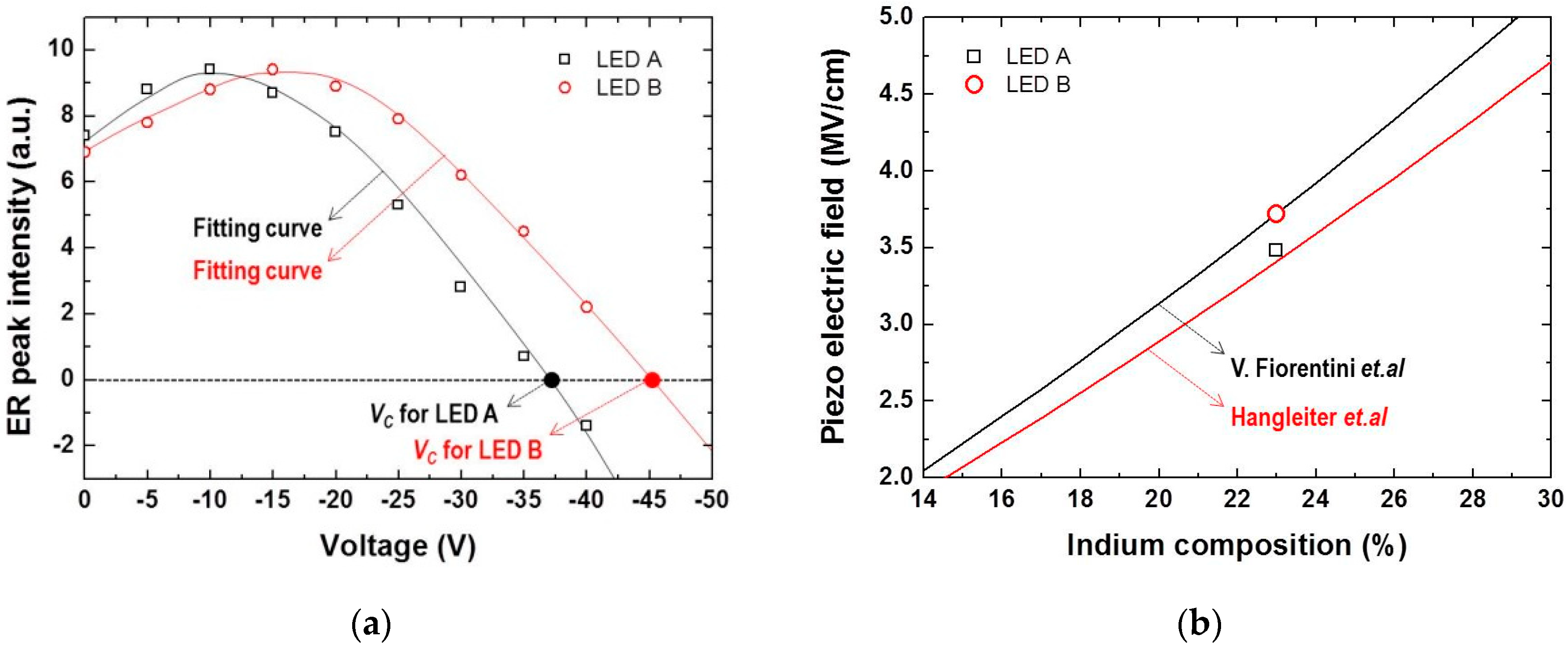
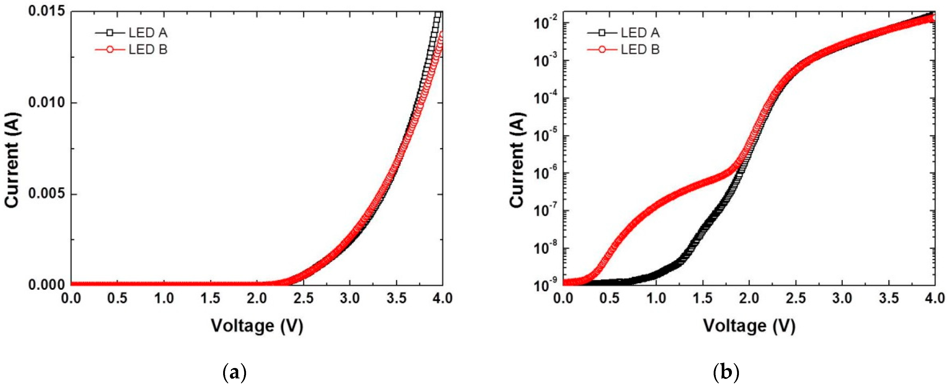
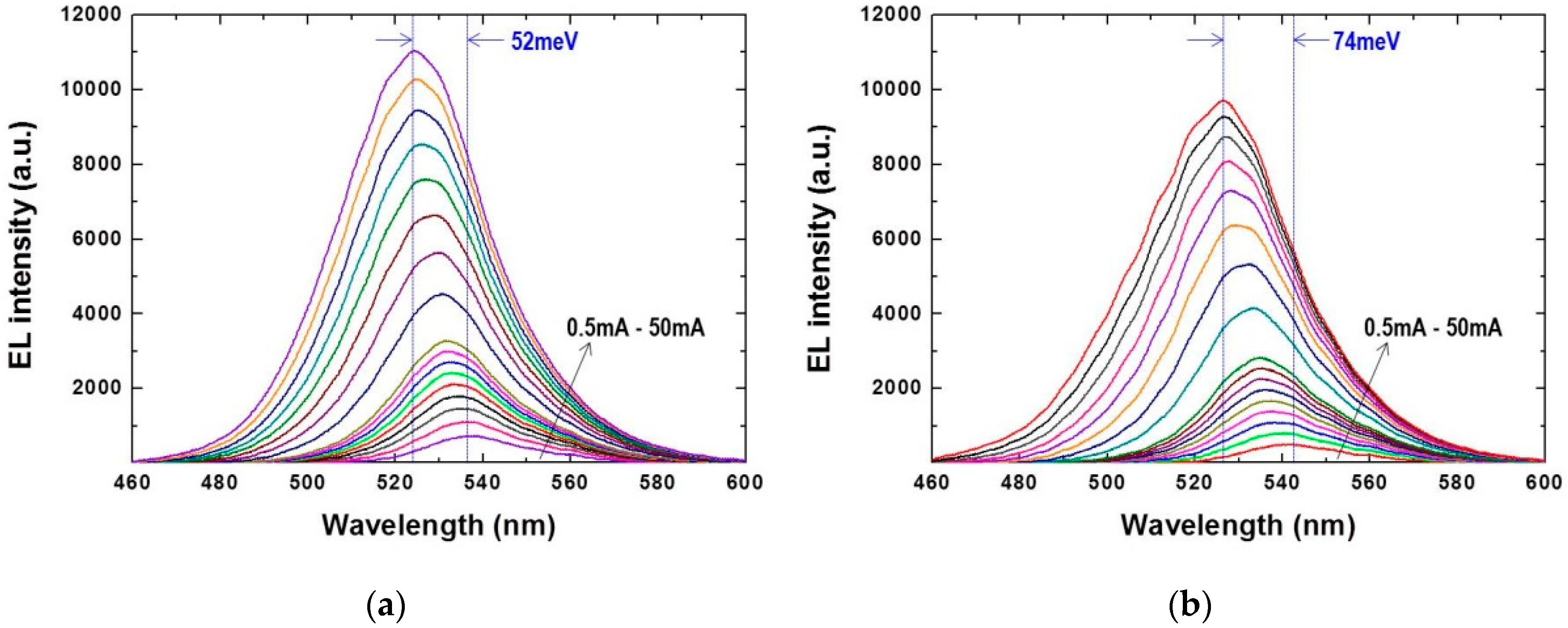
3. Results and Discussion

Previously, we reported that less strain in the u-GaN template layer can be achieved by replacing a conventional low temperature GaN buffer layer with a sputtered-AlN buffer layer on a c-plane sapphire substrate, where the crystalline quality of both samples was comparable [20]. Since the strain in the epitaxial layer after cooling down is greatly impacted by the strain of an adjacent layer during growth, one can thus infer that the strain and piezoelectric field in the MQWs active region is significantly influenced by the strain of the underlying layer [21,22,23]. In our structure, the epitaxial structure of the green LEDs is identical except for the buffer layer, thus, the strain in the u-GaN template layer can be considered a factor that limits the QCSE in the MQWs. To investigate the effect of the buffer layer on the piezoelectric field in the MQWs induced by strain, we experimentally measured the internal electric field of GaInN/GaN MQWs by means of reverse-biased ER spectroscopy. The detailed experimental set-up is described elsewhere [24]. The direction of the internal electric field induced by polarization in the GaInN/GaN MQWs grown on a c-plain sapphire substrate is opposite to that of the built-in electric field formed by a p-n junction [25]. Hence, the total internal electric field gradually decreases as the applied reverse bias increases. When the applied reverse bias reaches a compensation voltage (VC), a flat band condition is achieved. That is, one can then estimate the piezoelectric field by measuring VC. When the applied electric field further increases, i.e., V > VC, a phase inversion of the ER peak signal is expected [24,26]. In other words, investigating the peak intensity of the ER spectrum as a function of applied reverse bias, i.e., a phase inversion of the ER peak signal, is a useful way to measure VC [27].
Figure 2a shows the peak intensity in the ER spectra plotted against the applied reverse bias for LED A and LED B. A fifth-order polynomial function has been used to fit the experimental data and to estimate VC. The VC is determined by estimating a reverse-bias voltage at which point the fitting curve crosses zero [28]. Beyond this point, the peak intensity of the ER spectra turns negative, indicating a phase inversion of the ER signal. From the results in Figure 2a, the VC was estimated to be ~−38 V for LED A and ~−46 V for LED B.
Once VC is determined, the piezoelectric field (FPZ) can be obtained from the following equation [28]:
F P Z 2 ( V b i V C ) w ( V C ) ,
where Vbi is the built-in voltage and w(VC) is the depletion width at VC. Here, we selected 2.7 V as the Vbi and w(VC) was determined from the C–V curve. Note that C = εA/w, where C is the capacitance, ε is the dielectric constant, and A is the junction area [29]. From the C–V curve, w(VC) was estimated to be ~233 nm at −38 V for LED A and ~261 nm at −46 V for LED B. By combining the results for VC, Vbi, and w(VC), the FPZ was calculated to be ~3.48 MV/cm for LED A and ~3.72 MV/cm for LED B. The MQWs active layer are suffered from the compressive strain due to the difference in lattice mismatch between GaInN and GaN. Thus, measured piezo electric field in Figure 2b is caused by a compressive strain. The obtained FPZ values of the samples fall between the theoretical expectations reported by V. Fiorentini et al. [30] and Hangleiter et al. [31], as depicted in Figure 2b. That is, the obtained values of FPZ are reasonable considering the theoretical expected values (~3.72 MV/cm by V. Fiorentini et al. and ~3.41 MV/cm by Hangleiter et al. for 23% of GaN/GaInN strained layer). Therefore, we experimentally confirmed that the sputtered-AlN buffer layer of LED A leads to less strain and a lower FPZ in MQWs compared to that of a low temperature GaN buffer layer in LED B.
Next, to investigate the effect of the buffer layer on the electrical properties of the LEDs, we studied the I–V curves in linear and semi-log scales, see Figure 3a,b for LED A and LED B, respectively. No remarkable difference is observed in the linear scale graph (Figure 3a), while one can clearly observe in the semi-log scale graph (Figure 3b) that there is a different current component under low forward bias (from 0 V to 2 V).
There is no remarkable difference in the leakage current under reverse bias (results not shown in this paper). It is well-known that threading dislocations (TDs) and V-defects induce an additional current path that encourages leakage current by tunneling processes under low forward bias [32,33,34]. Thus, the larger leakage current under low forward bias is possibly due to higher TD and V-defect densities in MQWs of LED B. In general, the main contribution to the generation of dislocations and defects in a GaInN/GaN layer is the strain energy, namely, the strain energy is dissipated through the formation of a dislocation [35,36]. In this case, we infer that the larger strain energy of LED B introduces a higher density of TDs and V-defects, which eventually acts as a leakage current path and leads to tunneling leakage dominating the current flow under low forward bias, as shown in Figure 3b. Since the forward leakage current typically has a great impact on device reliability, electrostatic discharge characteristics, and ultimately device failure, one can say that a reliable LED device with a long lifetime could be expected by replacing a buffer layer with a sputtered-AlN layer [37].
Next, we investigated the optical properties by considering the EL spectrum dependence on the driving current for LED A and LED B (see Figure 4a,b). The wavelength at peak EL intensity (λpeak) was measured as ~536 nm for LED A and ~543 nm for LED B at 0.5 mA, and ~524 nm for LED A and ~526 nm for LED B at 50 mA. The blue shifts for LED A and LED B were ~52 meV and ~74 meV, respectively, namely, a larger blue shift of λpeak is observed in LED B. A blue shift that depends on driving current is typically caused by two mechanisms; (i) the QCSE and screening of the piezoelectric field owing to injected carriers [15], and (ii) the filling of the band-tail states by the injected carriers [29]. Here, we think that the QCSE is the dominant factor in this experimental result. The small blue shift in λpeak caused by less strain indicates some mitigation of the QCSE and a reduced piezoelectric field in LED A. Thus, we believe that this is further evidence of strain relaxation in MQWs by replacing a buffer layer with a sputtered-AlN layer.
Lastly, to investigate the emission performance of the LEDs, we measured the L–I and IQE–I curves of LED A and LED B, which are depicted in Figure 5a,b, respectively. Note that the measured light output power is a relative value. All light output powers of the LEDs in Figure 5a increase with increasing driving current. The light output powers of LED A and LED B are ~2.62 and ~1.91 at 50 mA, which indicates that the light output power of LED A is ~1.37 times greater than that of LED B. Note that the EQEs at 50 mA are estimated as ~15.8% and ~11.5% for LED A and LED B, respectively. Recently, we proposed a reliable and convenient method to determine the IQE of GaInN-based LEDs [38]. The method is based on finding an exact value of the light extraction efficiency (LEE) by analyzing the L–I curve with an advanced carrier dynamics equation, which obtains the IQE values by comparing the EQEs, i.e., IQE = EQE × LEE. The IQEs of the samples were evaluated by our proposed method and the results are shown in Figure 5b. A higher peak value of the IQE in LED A is observed, ~56% at 15 mA, compared to ~51% at 4 mA for LED B. The IQEs of LED A and LED B at 50 mA are ~52% and ~38% (a ~1.36-fold difference), which corresponds to the light output powers at 50 mA. This observation indicates that the LEEs of LED A and LED B are comparable. A more severe efficiency droop phenomenon (efficiency degradation from the peak of IQE to the IQE at 50 mA) is observed in LED B, i.e., ~4% for LED A and ~13% for LED B. These efficiency droop behaviors can be explained as follows: polarization sheet charges induced by strain at well-barrier interfaces lead to band bending which makes it potentially easier for carrier overflow from the MQWs to the p-side region [39,40]. In other words, the carrier overflow is enhanced by the energy barrier reduction by the strain, which results in a decrease in injection efficiency and consequently makes efficiency droop at a high injection current [41]. Therefore, the experimental results in Figure 5b, such as the IQE and efficiency droop behavior, are mainly determined from the piezoelectric field induced by strain. That is, the stronger FPZ of LED B than that of LED A in Figure 2 results in a more severe efficiency droop and degradation in emission performance.
Lastly, measured data of both samples are summarized and shown in Table 1 for the comparison.

4. Summary

In summary, we have demonstrated the electrical and optical performances of GaInN-based green LED devices with a sputtered-AlN buffer (LED A) and a conventional low temperature GaN buffer layer (LED B). We experimentally confirmed by means of reverse bias ER spectroscopy and the smaller blue shift in the EL spectrum that there is a larger reduction in the piezoelectric field in LED A compared to that of LED B (approximately 9%). The I–V curve shows different conduction process in the low forward bias region, i.e., tunneling leakage dominates the current in LED B, which is due to the generation of TDs and V-defects that relax the strain energy. These defects are fatal to device reliability and lifetime. We obtained ~56% and ~51% of the peak IQE, and ~52% and ~38% of IQE at 50 mA, and ~4% and ~13% efficiency droops for LED A and LED B, respectively. We believe that the improvement in IQE and light output power is due to a reduction in carrier overflow which is limited by the strain and the piezoelectric field in MQWs. We show that the crystalline quality and strain in the active region can be improved by just replacing the buffer layer, which eventually contributes to high performance and reliability of the LED device. Therefore, we can conclude that replacing a conventional low temperature GaN buffer layer with a sputtered-AlN buffer layer is a very effective way for improving device performance, such light output power, and the IQE of green GaInN-based LEDs. Additionally, it can be expected that the reliability and lifetime could also be improved. We believe that further improvements can be achieved by the optimization of a sp-AlN buffer layer such as thickness and sputtering power.

Author Contributions

S.I., D.-P.H., K.Y. and R.M. conducted the experiments and data analysis under the advising of S.K., T.T., M.I. and I.A.; D.-P.H. and S.I. mainly wrote the manuscript; S.K. read, edited and commented on the manuscript.

Funding

This research is supported by MEXT Private University Research Branding Project and JSPS KAKENHI for Innovative Areas [No.16H06416].

Acknowledgments

Authors would like to thank Gyeong Won Lee and Sang-Jin Min at Hanyang University, Korea for supporting of ER measurement. This work was supported by MEXT Private University Research Branding Project, MEXT Program for research and development of next-generation semiconductor to realize energy-saving society, JSPS KAKENHI for Scientific Research A [No.15H02019], JSPS KAKENHI for Scientific Research A [No.17H01055], JSPS KAKENHI for Innovative Areas [No.16H06416], and Japan Science and Technology CREST [No.16815710].

Conflicts of Interest

The authors declare no conflict of interest.

References

  1. Amano, H. Nobel Lecture: Growth of GaN on sapphire via low-temperature deposited buffer layer and realization of p-type GaN by Mg doping followed by low-energy electron beam irradiation. Rev. Mod. Phys. 2015, 87, 1133–1138. [Google Scholar] [CrossRef]
  2. Tsao, J.Y.; Wierer, J.J., Jr.; Rohwer, L.E.S.; Coltrin, M.E.; Crawford, M.H.; Simmons, J.A.; Hung, P.-C.; Saunders, H.; Sizov, D.S.; Bhat, R.; et al. Introduction Part B. Ultra-efficient solid-state lighting: Likely characteristics, economic benefits, technological approaches. In III-Nitride Based Light Emitting Diodes and Applications; Seong, T.-Y., Han, J., Amano, H., Morkoç, H., Eds.; Springer: Dordrecht, The Netherlands, 2013; pp. 11–26. ISBN 978-94-007-5862-9. [Google Scholar]
  3. Liu, B.; Nie, H.; Zhou, X.; Hu, S.; Luo, D.; Gao, D.; Zou, J.; Xu, M.; Wang, L.; Zhao, Z.; et al. Manipulation of Charge and Exciton Distribution Based on Blue Aggregation-Induced Emission Fluorophors: A Novel Concept to Achieve High-Performance Hybrid White Organic Light-Emitting Diodes. Adv. Funct. Mater. 2016, 26, 776–783. [Google Scholar] [CrossRef]
  4. Ikeyama, K.; Kozuka, Y.; Matsui, K.; Yoshida, S.; Akagi, T.; Akatsuka, Y.; Koide, N.; Takeuchi, T.; Kamiyama, S.; Iwaya, M.; et al. Room-temperature continuous-wave operation of GaN-based vertical-cavity surface-emitting lasers with n-type conducting AllnN/GaN distributed Bragg reflectors. Appl. Phys. Express 2016, 9, 102101. [Google Scholar] [CrossRef]
  5. Razeghi, M.; Rogalski, A. Semiconductor ultraviolet detectors. J. Appl. Phys. 1996, 79, 7433–7473. [Google Scholar] [CrossRef]
  6. Kurokawa, H.; Kaga, M.; Goda, T.; Iwaya, M.; Takeuchi, T.; Kamiyama, S.; Akasaki, I. Multijunction GaInN-based solar cells using a tunnel junction. Appl. Phys. Express 2014, 7, 034104. [Google Scholar] [CrossRef]
  7. Nakamura, S.; Fasol, G. The Blue Laser Diode: GaN Based Light Emitters and Lasers; Springer: Berlin/Heidelberg, Germany, 1997; pp. 1–335. ISBN 978-3-662-03464-4. [Google Scholar]
  8. Amano, H.; Sawaki, N.; Akasaki, I.; Toyoda, Y. Metalorganic vapor phase epitaxial growth of a high quality GaN film using an AIN buffer layer. Appl. Phys. Lett. 1986, 48, 353–355. [Google Scholar] [CrossRef]
  9. David, A.; Hurni, C.A.; Young, N.G.; Graven, M.D. Electrical properties of III-Nitride LEDs: Recombination-based injection model and theoretical limits to electrical efficiency and electroluminescent cooling. Appl. Phys. Lett. 2016, 109, 083501. [Google Scholar] [CrossRef] [Green Version]
  10. Saito, S.; Hashimoto, R.; Hwang, J.; Nunoue, S. InGaN Light-emitting diodes on c-Face sapphire substrates in green gap spectral range. Appl. Phys. Express 2013, 6, 111004. [Google Scholar] [CrossRef]
  11. Crawford, M.H. LEDs for solid-state lighting: Performance challenges and recent advances. IEEE J. Sel. Top. Quantum Electron. 2009, 15, 1028–1040. [Google Scholar] [CrossRef]
  12. Holec, D.; Costa, P.M.F.J.; Kappers, M.J.; Humphreys, C.J. Critical thickness calculations for InGaN/GaN. J. Cryst. Growth 2007, 303, 314–317. [Google Scholar] [CrossRef]
  13. Doi, T.; Honda, Y.; Yamaguchi, M.; Amano, H. Strain-compensated effect on the growth of InGaN/AlGaN multi-quantum well by metalorganic vapor phase epitaxy. Jpn. J. Appl. Phys. 2013, 52, 08JB14. [Google Scholar] [CrossRef]
  14. der Maur, M.A.; Pecchia, A.; Penazzi, G.; Rodrogies, W.; Carlo, A.D. Efficiency drop in green InGaN/GaN light emitting diodes: The role of random alloy fluctuations. Phys. Rev. Lett. 2016, 116, 027401. [Google Scholar] [CrossRef] [PubMed]
  15. Takeuchi, T.; Sota, S.; Satusragawa, M.; Komori, M.; Takeuch, H.; Amano, H.; Akasaki, I. Quantum-confined Stark effect due to piezoelectric fileds in GaInN strained quantum wells. Jpn. J. Appl. Phys. 1997, 36, L382–L385. [Google Scholar] [CrossRef]
  16. Xia, Y.; Hou, W.; Zhao, L.; Zhu, M.; Detchprohm, T.; Wetzel, C. Boosting green GaInN/GaN light-emitting diode performance by a GaInN underlying layer. IEEE Trans. Electron Dev. 2010, 57, 2639–2643. [Google Scholar] [CrossRef]
  17. Iida, D.; Lu, S.; Hirahara, S.; Niwa, K.; Kamiyama, S.; Ohkawa, K. Enhanced light output power of InGaN-based amber LEDs by strain-compensating AlN/AlGaN barriers. J. Cryst. Growth 2016, 448, 105–108. [Google Scholar] [CrossRef]
  18. Taksuka, D.; Akatsuka, Y.; Ino, M.; Koide, N.; Takeuchi, T.; Kamiyama, S.; Iwaya, M.; Akasaki, I. GaInN-based tunnel junctions with graded layers. Appl. Phys. Express 2016, 9, 081005. [Google Scholar] [CrossRef]
  19. Park, J.-Y.; Lee, J.-H.; Jung, S.; Ji, T. InGaN/GaN-based green-light-emitting diodes with an inserted InGaN/GaN-graded superlattice layer. Phys. Status Solidi A 2016, 213, 1610–1614. [Google Scholar] [CrossRef]
  20. Ishimoto, S.; Han, D.-P.; Yamamoto, K.; Kamiyama, S.; Takeuchi, T.; Iwaya, M.; Akasaki, I. Improvement of Emission Efficiency with Sputtered AlN Buffer Layer in GaInN-based Light-emitting Diodes. Jpn. J. Appl. Phys. 2019, in press. [Google Scholar]
  21. Shioda, T.; Yoshida, H.; Tachibana, K.; Sugiyama, N.; Nunoue, S. Enhanced light output power of green LEDs employing AlGaN interlayer in InGaN/GaN MQW structure on sapphire (0001) substrate. Phys. Status Solidi A 2012, 209, 473–476. [Google Scholar] [CrossRef]
  22. Lee, K.; Lee, C.-R.; Lee, J.H.; Chung, T.-H.; Ryu, M.-Y.; Jeong, K.-U.; Leem, J.-Y.; Kim, J.S. Influences of Si-doped graded short-period superlattice on green InGaN/GaN light-emitting diodes. Opt. Express 2016, 24, 7743–7751. [Google Scholar] [CrossRef] [PubMed]
  23. Nakao, T.; Fujii, T.; Sugiyama, T.; Yamamoto, S.; Iida, D.; Iwaya, M.; Takeuchi, T.; Kamiyama, S.; Akasaki, I.; Amano, H. Fabrication of nonpolar a-plane nitride-based solar cell on r-Plane sapphire substrate. Appl. Phys. Express 2011, 4, 101001. [Google Scholar] [CrossRef]
  24. Usman, M.; Kim, H.; Shim, J.-I.; Shin, D.-S. Measurement of piezoelectric field in single- and double-quantum-well green LEDs using electroreflectance spectroscopy. Jpn. J. Appl. Phys. 2014, 53, 098002. [Google Scholar] [CrossRef]
  25. Takeuchi, T.; Amano, H.; Akasaki, I. Theoretical study of orientation dependence of piezoelectric effects in wurtzite strained GaInN/GaN heterostructures and quantum wells. Jpn. J. Appl. Phys. 2000, 39, 413–416. [Google Scholar] [CrossRef]
  26. Wetzel, C.; Takeuchi, T.; Akasaki, I. Piezoelectric Franz–Keldysh effect in strained GaInN/GaN heterostructures. J. Appl. Phys. 1999, 85, 3786–3791. [Google Scholar] [CrossRef]
  27. Hsu, T.M.; Lai, C.Y.; Chang, W.-H.; Pan, C.-C.; Chuo, C.-C.; Chyi, J.-I. Electroreflectance study on the polarization field in InGaN/AlInGaN multiple quantum wells. Appl. Phys. Lett. 2004, 84, 1114–1116. [Google Scholar] [CrossRef]
  28. Song, J.-H.; Kim, T.-S.; Park, K.-N.; Lee, J.-G.; Hong, S.-K.; Choi, S.-R.; Lee, S.; Cho, M.W. Experimental verification of effects of barrier dopings on the internal electric fields and the band structure in InGaN/GaN light emitting diodes. Appl. Phys. Lett. 2014, 104, 121114. [Google Scholar] [CrossRef]
  29. Han, D.-P.; Shim, J.-I.; Shin, D.-S.; Kim, K.-S. Effects of unbalanced carrier injection on the performance characteristics of InGaN light-emitting diodes. Appl. Phys. Express 2016, 9, 081002. [Google Scholar] [CrossRef]
  30. Fiorentini, V.; Bernardini, F.; Ambacher, O. Evidence for nonlinear macroscopic polarization in III–V nitride alloy heterostructures. Appl. Phys. Lett. 2002, 80, 1204–1206. [Google Scholar] [CrossRef]
  31. Hangleiter, A.; Hitzel, F.; Lahmann, S.; Rossow, U. Composition dependence of polarization fields in GaInN/GaN quantum wells. Appl. Phys. Lett. 2003, 83, 1169–1171. [Google Scholar] [CrossRef]
  32. Han, D.-P.; Oh, C.-H.; Kim, H.; Shim, J.-I.; Kim, K.-S.; Shin, D.-S. Conduction mechanisms of leakage currents in InGaN/GaN-based light-emitting diodes. IEEE Trans. Electron Dev. 2015, 62, 587–592. [Google Scholar]
  33. Kim, J.; Kim, J.; Tak, Y.; Chae, S.; Kim, J.-Y.; Park, Y. Effect of V-shaped pit size on the reverse leakage current of InGaN/GaN light-emitting diodes. IEEE Electron Dev. Lett. 2013, 34, 1409–1411. [Google Scholar] [CrossRef]
  34. Cao, X.A.; Stokes, E.B.; Sandvik, P.M.; LeBoeuf, S.F.; Kretchmer, J.; Walker, D. Diffusion and tunneling currents in GaN/InGaN multiple quantum Well light-emitting diodes. IEEE Electron Dev. Lett. 2002, 23, 535–537. [Google Scholar] [CrossRef]
  35. Iwaya, M.; Yamamoto, T.; Iida, D.; Condo, Y.; Sowa, M.; Matsubara, H.; Ishihara, K.; Takeuchi, T.; Kamiyama, S.; Akasaki, I. Relationship between misfit-dislocation formation and initial threading-dislocation density in GaInN/GaN heterostructures. Jpn. J. Appl. Phys. 2015, 54, 115501. [Google Scholar] [CrossRef]
  36. Iida, D.; Condo, Y.; Sowa, M.; Toru, S.; Iwaya, M.; Takeuchi, T.; Kamiyama, S.; Akasaki, I. Analysis of strain relaxation process in GaInN/GaN heterostructure by in situ X-ray diffraction monitoring during metalorganic vapor-phase epitaxial growth. Phys. Status Solidi RRL 2013, 7, 211–214. [Google Scholar] [CrossRef]
  37. Meneghini, M.; Tazzoli, A.; Mura, G.; Meneghesso, G.; Zanoni, E. A Review on the physical mechanisms that limit the reliability of GaN-based LEDs. IEEE Trans. Electron Dev. 2010, 57, 108–118. [Google Scholar] [CrossRef]
  38. Han, D.-P.; Yamamoto, K.; Ishimoto, S.; Mano, R.; Iwaya, M.; Takeuchi, T.; Kamiyama, S.; Akasaki, I. Determination of Internal Quantum Efficiency in GaInN-based Light-emitting Diode under Electrical Injection: Carrier Recombination Dynamics Analysis. Appl. Phys. Express 2019, 12, 032006. [Google Scholar] [CrossRef]
  39. Kim, M.-H.; Schubert, M.F.; Dai, Q.; Kim, J.K.; Schubert, E.F. Origin of efficiency droop in GaN-based light-emitting diodes. Appl. Phys. Lett. 2007, 91, 183507. [Google Scholar] [CrossRef] [Green Version]
  40. Ryu, H.-Y. Effect of internal polarization fields in InGaN/GaN multiple-quantum wells on the efficiency of blue light-emitting diodes. Jpn. J. Appl. Phys. 2012, 51, 09MK03. [Google Scholar] [CrossRef]
  41. Han, D.-P.; Shim, J.-I.; Shin, D.-S. Analysis of carrier recombination dynamics in InGaN-based light-emitting diodes by differential carrier lifetime measurement. Appl. Phys. Express 2017, 10, 052101. [Google Scholar] [CrossRef]
Figure 1. Schematic illustrations of (a) GaInN-based green light-emitting diode (LED) with a sputtered-AlN buffer layer (LED A) (b) GaInN-based green LED with a conventional LT-GaN buffer layer (LED B). The inset of Figure 1a is the top-view image of both samples and the inset of Figure 1b is the top-view image of electroluminescence (EL) emission for both samples.
Applsci 09 00788 g001
Figure 2. (a) The peak intensity of the ER spectra and the fitting curves plotted against the applied reverse bias for LED A and LED B. (b) Measured piezoelectric field values (dots) and the theoretically calculated values (solid lines).
Applsci 09 00788 g002
Figure 3. Current-voltage characteristics (I–V curve) for LED A and LED B (a) linear scale and (b) in semi-log scale.
Applsci 09 00788 g003
Figure 4. Electroluminescence (EL) spectrum dependence on driving current of (a) LED A and (b) LED B.
Applsci 09 00788 g004
Figure 5. Results of (a) light output power-current characteristics (L–I curve) and (b) internal quantum efficiency-current characteristics (IQE–I curve) for LED A and LED B on a linear scale.
Applsci 09 00788 g005
Table 1. Measured data of LED A and LED B.
SamplePiezoelectric Field
[MV/cm]
Blue Shift
[meV]
IQE at 50 mA
[%]
Efficiency Droop
[%]
LED A~3.4852524
LED B~3.72743813

