1. Introduction
Metamaterials are artificial structures or assemblies specially designed to reach specific properties that natural materials do not have [
1]. Artificial media can be created by different means, among which additive manufacturing offers several advantages for making objects with a complex shape [
2,
3]. Before adopting a new manufacturing process such as 3D printing, the merit of the process must be evaluated with care. Sustainability criteria are becoming more and more stringent in the process assessment. Reduced consumption of both energy and natural resources, a small volume of waste, environmental issues, life cycle of the manufactured products, etc., must be weighted with specific tools against other constraints, such as cost and ease of production, human labor, etc. [
4]. Among the advantages of additive manufacturing, one may cite (i) the possibility to produce a large variety of prototypes or functional components with complex geometry, (ii) substantial automation of the technological process, and (iii) a reduction in the number of manufacturing steps [
5,
6,
7]. Disadvantages include (i) the limited number of materials that can be involved in the process, (ii) a longer fabrication time, and (iii) a higher energy consumption in comparison with conventional methods.
Due to its advantages, additive manufacturing is actively used in diverse such areas as aerospace, automotive, medical, architecture, education, etc. [
8]. Different 3D printing technologies include stereolithography [
3,
9] and extrusion printing method [
10]. The latter approach has been successfully applied to produce conductive cellular structures [
10,
11]. For this production, ink made of polymer with embedded conductive inclusions at a concentration above the percolation threshold is used. Despite the low cost and wide prevalence of 3D printing technology based on extrusion of polymer material, this method is limited to the production of overhanging structures. It requires special support media that complicate the manufacturing process [
12]. In contrast, the selective laser sintering fabrication process can deal with a shape sample of any complexity. It can potentially be applied for the fabrication of 3D cellular structures with, however, a larger mass of material used in the fabrication process [
13].
Nowadays, sub-mm spatial resolution can easily be reached with commercially-available printers. At this length scale and above, one may think of myriads of mechanical, acoustical, electrical, etc., applications, including the fabrication of molds for the manufacture of special pieces [
4]. In particular, 3D printing is providing new opportunities for the fabrication of electromagnetic metamaterials with unusual behavior for electromagnetic radiation in the radio wave and microwave domains [
14,
15]. For instance, suitably-structured dielectrics behave like an effective anisotropic media for microwaves [
16]; a periodic array of small metallic inclusions in a polymer matrix may be seen as a diamagnetic effective medium [
17]. When deposited on a metallic foil, 3D-printed all-dielectric resonators lead to broad-band absorption in the microwave range [
18,
19]. Many other applications are under investigation, which range from DC electrical circuits [
20] to GHz antennas [
21].
The structure of interest in this work is a periodic network of interconnected beams defining a 3D mesh.
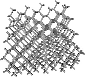
Figure 1 is an example representing a diamond lattice. Light 3D lattices of that kind can easily be produced by additive manufacturing [
22,
23], including the largely-diffused 3D-printing technology based on polymer materials, such as fused deposition modeling (FDM). Recent examples of FDM products are: Kagome mesh structures made of acrylonitrile butadiene styrene (ABS) polymer [
24] and simple-cubic lattices made of conducting nanocarbon-doped polylactic acid (PLA) [
25]. In that case, the lattice parameter is a few millimeters wide or larger. The advantages of incorporating lattice structures in mechanical parts is so obvious [
26] that commercial 3D printing software includes this feature. Moreover, strategies for optimizing the lattice geometry specifically for additive manufacturing have been proposed [
27]. From the mechanical point of view, a three-dimensional frame of struts just meeting at nodes must have a nodal connectivity
Z greater than five to ensure structural stability [
28]. This rule does not hold when the structural elements are intimately welded as they are with 3D printing. In fact, lattices manufactured by 3D printing combine light weight and remarkable mechanical properties [
29,
30]. Whereas lattice structures combine many properties of foams, it has been argued that 3D-printed lattice structures may outperform foam materials of the same porosity [
31].
A plastic 3D mesh manufactured by FDM can conduct electricity when the polymer filament that feeds the printer has been loaded with nanoscopic conducting inclusions at a concentration above the percolation threshold [
11,
20,
32]. Polymer-based resistive lattices have potential applications as 3D stretchable conductors [
33]. They are also interesting media for electromagnetic (em) applications owing to their lower conductivity compared to metallic networks. As a consequence, only a small fraction of incoming em radiations is reflected; the rest enters the structure while being progressively absorbed. The shielding structure does not need to be earthed, because the em attenuation is due to power loss produced by Joule heating. Inspired by research works on disordered 2D networks of metallic nanowires [
34] or on 3D percolation networks in composite polymers [
35], one may infer that an artificial lattice of conducting elements may offer protection against electrostatic discharges or be efficient to shield electromagnetic perturbations. In the latter case, absorption resonances are expected to happen for wavelengths of the order of, or shorter than, the unit cell size [
36].
In the present paper, by combining the theory of resistor networks [
37] and classical continuous-medium electrodynamics, a new formulation of the electrokinetic behavior of a conducting lattice is derived. Due to the length scale provided by the lattice parameter, the effective continuous medium that mimics the electrokinetic response of a resistor lattice is characterized by a non-local Ohm’s law.
2. Background
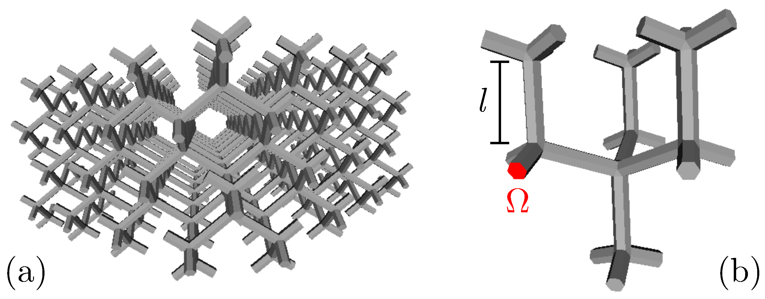
Figure 1 shows a model of a mesh having the diamond structure designed for 3D printing technology. The mesh can be viewed as a periodic duplication of the structural unit detailed in Panel (b). The mesh is composed of conducting rods interconnected at nodes. Each rod has a prismatic shape (hexagonal prism in
Figure 1). A node is defined as the volume where crossing rods meet. In
Figure 1, the nodes are truncated tetrahedra. The mesh can be treated as a discrete network of resistors under the assumption that each node is an equipotential body. The latter assumption is valid either when the lateral dimensions of the rods are much smaller than their length or if each node is made of a perfectly-conducting medium. Then, a single potential can be attributed to each node. Under this condition, the resistance of a rod is
with
l and
being the length and cross-sectional area (see
Figure 1b), respectively, and
being the conductivity of the polymer nanocomposite used for the fabrication. The mesh can therefore be considered as a network of resistors [
38].
The nodes of the mesh receive discrete labels
. If
is the current injected at node
i from an external source, combining Kirchhoff and Ohm’s laws yields:
where
if
i and
j are connected by a rod of resistance
,
otherwise, and
. Obviously, the admittance matrix
, also called the Laplacian matrix [
39], is singular. This prevents one to solve Equation (
1) directly for
. The difficulty can be tackled by assuming that each node is connected to an external ground electrode, whose potential is set to zero, by a constant admittance
y. The limit
will be taken at the end of the calculations. With this trick in hand, Equation (
1) is replaced by:
Now, the set of equations (
2) for
can be solved for the node potentials
in the form:
with
being the elements of the resolvent matrix
. The resolvent matrix is symmetric. It is perfectly defined whenever
y is outside the set of eigenvalues of
L, in particular for any real positive value of
y.
When the mesh is a regular infinite lattice where all nodes are equivalent and all rods have the same resistance
R, the resolvent matrix is related to the topological lattice Green’s function [
40]
where
is the adjacency matrix, defined as
when the nodes
i and
j are directly connected and zero otherwise including when
. The relation between the matrices is
where
Z is the lattice coordination number. With the help of Bloch’s theorem, a spectral representation of
for 2D and 3D lattices is available in the form of 2D and 3D integrals in Fourier space, to which belong the so-called Watson integrals [
41]. Due to the translational symmetry of the lattice, the diagonal elements
all take on the same value. For 2D lattices, the diagonal elements of
diverge like
when
, which corresponds to the limit
of relevance here. For 3D lattices, the limit of
for
is a finite number
listed in
Table 1. There is a simple 1/4 factor between the
values of the fcc and diamond lattices [
42].
The equivalent resistance of the mesh seen from two nodes
m and
n, also called two-point resistance [
43], is defined as the ratio
when the current
I is injected at node
m and removed from node
n. A simple application of Equation (
3) yields:
after the limit
has been taken and given that
is a symmetric matrix. The limit
of individual elements of the resolvent matrix may be difficult to evaluate, especially in 2D. One can get rid of this difficulty by rewriting the right-hand side of Equation (
4) as a diagonal element of the resolvent matrix [
38]. Values of
can be obtained analytically for a few simple 3D lattices: sc [
44], bcc [
45], fcc [
46] (the equivalent resistances tabulated in [
46] must be divided by a factor of two), and diamond [
47].
By construction,
when
. The equivalent resistance between two nodes infinitely far away is
[
41].
3. Continuous Medium Approximation
The aim of this section is to transform the electrokinetic equations of a continuous medium so as to reproduce the main characteristics of an infinite discrete 3D lattice of resistors with constant resistance R. It is implicitly assumed that all the nodes of the lattice are equivalent (mono-atomic-like crystal lattice).
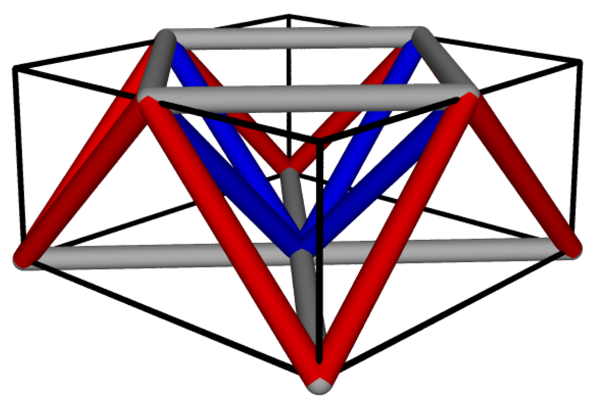
The first objective is to assign an apparent bulk conductivity to the resistor lattice. For a simple cubic lattice in
d-dimensional-space and parameter
a, the apparent resistivity is
[
44].
Figure 2 sketches how an apparent resistivity can be obtained for a resistive mesh with fcc lattice. Half a conventional cubic unit cell is shown. The nodes located in the basal plane are grounded to potential zero. The nodes located in the upper horizontal plane are at potential
V. The current flows across the non-horizontal rods. All have the same resistance
R and are assembled in parallel. Each of the height red rods, being shared by two adjacent cells, must be viewed as two parallel resistors of resistances
, one per each face-sharing unit cell. Accordingly, the total resistance experienced by the current flowing through half the unit cell shown in
Figure 2 is
. The same half unit cell, viewed as a continuous medium of resistivity
, height
, and basis area
would have a resistance
, where
a is the fcc lattice parameter. Consequently,
for the fcc mesh. The apparent resistivity obtained the same way for other lattices is given in
Table 1.
If the current
I is injected on a given node, referred to as “Node 0”, Equation (
3) gives the potential
on any node
m compared to the zero potential of the ground electrode each node is connected through the fictitious admittance
y. Accordingly, for any positive value of
y, the current cannot spread on the network to infinity, and
vanishes when the distance between Nodes
m and 0 increases to infinity. This property remains at the limit
with the consequence:
Setting
, one obtains the potential of the contact node
, which is finite for a 3D lattice as mentioned above (see
Table 1).
In the same condition, the potential at location
produced in a continuous medium by a point source injecting the current
I at position
is
. Similar to the case of the discrete lattice, this expression for the potential vanishes at infinity. Unlike the case of the discrete lattice, the potential at the contact point is infinite. Therefore, the Coulomb-like law has to be corrected for short distances, by writing:
with
and
the positions of Sites
m and 0 on the lattice.
is a correction function that vanishes like
at the limit
so as to balance the Coulomb singularity. Comparing Equation (
5) for
and Equation (
6) for
allows one to set:
Combining Equations (
4)–(
7), the two-point resistance can be recast as:
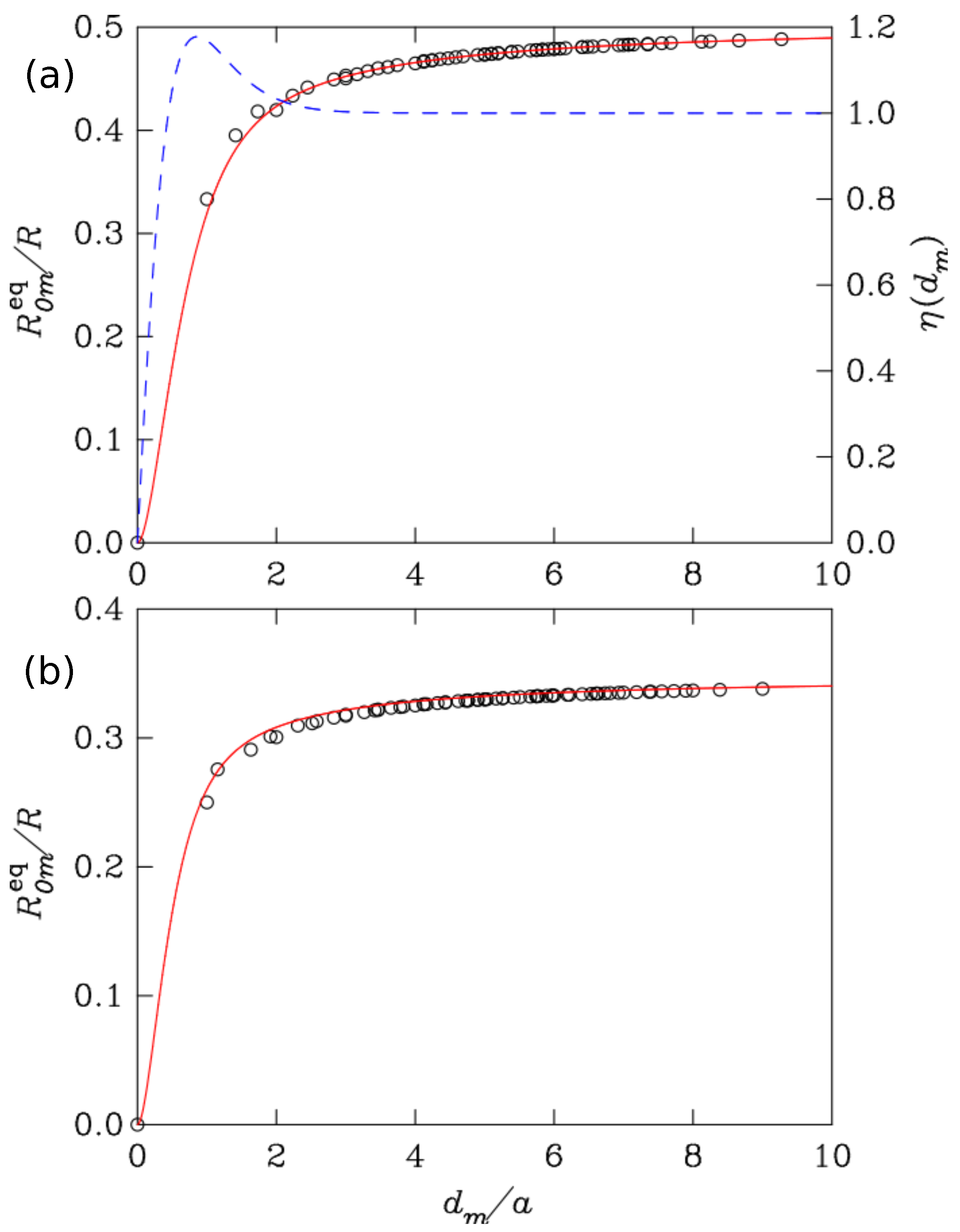
The open circle symbols in
Figure 3 represent the equivalent resistances between pairs of nodes of the simple cubic and body-centered cubic resistor lattices up to a distance of nine-times the cubic lattice parameter
a. Although the pairs of nodes are oriented along various crystallographic directions, the equivalent-resistance data chiefly fall around a single monotonous curve of the separation distance
. For these cubic lattices, one may then ignore the existence of tiny anisotropic variations and consider that the correction function
is a function of the distance
. Setting from now on:
yields:
At the bond length distance
, the equivalent resistance is
[
48], with
Z the lattice coordination as above. Accordingly, Equation (
10) tells one that:
The values of
and
for cubic lattices are listed in
Table 1.
Having a continuous-medium approximation in mind, one considers
as a continuous parameter. At a large distance, the discrete character of the resistor lattice should play no role, with the consequence
. At the other end, it has already been established through the definition of
(Equation (
7)) that
for
. At the bond length distance,
Table 1 indicates that
.
Summing up the information gained thus far, the function
increases for small
x, reaches a maximum above unity, and eventually approaches one asymptotically. The shape of the function
can be sketched; see the dashed-line curve plotted in
Figure 3. For reasons that will be made clear below, one will further impose
. A simple function that reproduces all these characteristics is:
The full-line curves in
Figure 3 illustrate how well this function works for the simple cubic and body-centered cubic resistor lattices. Even if a better representation of the two-point resistance versus distance could be achieved based on more sophisticated expressions of
, additional terms in
would make it possible to reproduce the exact value given by Equation (
11) for
. Equation (
12) will be sufficient for what follows.
When a given set of nodes
m of the resistor lattice is fed by a given set of currents
, a current source function can be defined as
. With this definition in hand, the resulting potential of the lattice nodes readily follows from Equation (
6):
where
can conveniently be viewed as a continuous variable, although it strictly stands for the position of the nodes of the system. When writing this equation, it has been assumed that the correction function
is a function of the distance
.
The last equations will be applied to a lattice portion having the shape of a slab whose top and bottom faces are two parallel crystallographic planes. All the nodes of the mesh located on and above the top face of the slab are supposed to be held at the potential
, while the nodes located on and below the bottom face are held at the potential
. Under the assumption of monoatomic lattice, all the nodes located on each ending face are equivalent and receive the same current
on the top and
at the bottom. Each crystallographic plane parallel to the ending faces of the slab is an equipotential surface. From now on, the mesh is treated as a continuous medium. In particular, the slab is seen as a disk of radius
and height
L. The source function is given by
with
z being the axial coordinate and
, where
A is the area of the two-dimensional periodic unit cell of the ending lattice faces. The potential (Equation (
13)) of a point located on the axis of the slab at a distance
z from the bottom basis is:
with
and
. Having realized that
, one obtains:
In particular,
where Equation (
9) has been used to transform the last term between
in the right-hand side of the last expression. This last term rapidly vanishes with increasing
thanks to the integral property imposed on the function
. With the expression (Equation (
12)) of
, the result
is recovered as soon as
L is larger than
, which is already the case after one lattice parameter
a (see
Table 1). This is an important outcome, because the apparent resistivity
of a resistor lattice was defined exactly according to the usual relationship between
and
j.
4. Ohm’s Law
The continuous-medium description of a lattice mesh obtained thus far reproduces some important electrokinetic properties of the latter. Even though the electrokinetics of a network of resistors is governed by topology much more than by geometry, it is tempting to explore the continuous-medium approach slightly further. Forgetting the discrete nature of the interconnected rods, a microscopic Ohm’s law will be derived for the continuous medium that would respond to a current source distribution according to Equation (
13). Ohm’s law is first derived in Fourier space. A non-local form of Ohm’s law in real space will be obtained afterward by back Fourier transform of the results obtained. Taking the Fourier transform of Equation (
13) versus
yields:
where
and
are the Fourier transforms of
and
, respectively.
In the stationary case,
and
. In Fourier space,
and
with
and
the Fourier transforms of the electric field and the current density, respectively. Inserting these expressions into Equation (
17) yields:
The set of factors on the left-hand side of the dot product symbol represents the resistivity tensor:
Using the definition of
(Equation (
17)) and assuming as here above that
is a function of the distance
r irrespective of the direction of
leads one to:
The last term follows from Equation (
9) along with the mathematical model provided by Equation (
12).
A back-Fourier transform of Equation (
18) allows one to write the electric field in real space as a convolution of the current density. The result is:
with
,
being the identity tensor. This expression is the main result of the paper. It gives the macroscopic electric field at location
due to the actual distribution of current density.
In order to catch the content of the obtained non-local Ohm’s law for an infinite medium, let us consider a uniform flow of
in one direction, taken as the
z axis, with an intensity
depending on the
z coordinate only. The integral over
in Equation (
21) can be performed in cylindrical coordinates around the axis parallel to
z passing through the local position
. It is easy to show that the electric field will be oriented along
z with a component that depends on
z only. Working as for Equation (
15), one is led to:
The integration over the variable
R is readily carried out to give the simple analytical result:
where
is the derivative of the function
with respect to its argument. As a simple illustration, the current density is supposed to be a constant
j in the half space
and zero in the half space
. This situation would be realized if there were a current source uniformly distributed on the plane
and a current drain localized on a parallel plane at
. Taking into account the properties
and
, one obtains:
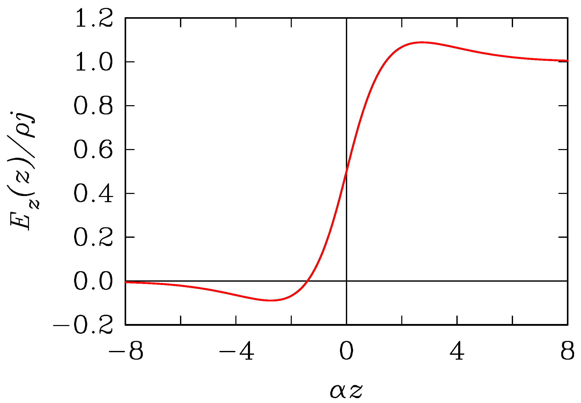
As shown in
Figure 4, the electric field rapidly converges to
in the half space that sustains the current and rapidly vanishes in the half space where there is no current. Still, the transition at the interface
is not infinitely sharp, but extends over a region of width
. The minima and maxima of the electric field are due to the maximum that the correction function
must have, as discussed above. With the simple analytical representation used here (Equation (
12)), the extrema of
take place at
. This value can be considered as a penetration depth of the electric field in a region where the current density is zero.
It can be useful to recast Equation (
21) in the following form:
after the first term, which corresponds to a normal 3D resistive medium, has been extracted. If the right-hand side were limited to this sole first term, the equation obtained would be equivalent to
after
were replaced by
, with
. The second part of Equation (
26) is a correction to Ohm’s law coming from the discrete structure of the resistive mesh. The correction term is still a convolution product, like Equation (
21), now with a kernel that samples a narrow region around the position
, with radius of the order of
. If the current density varies slowly with
on the scale
, it can be expended in a power series of
restricted to its first few terms. Each term can be integrated over
. Carrying on this development is easy in Fourier space, starting from Equation (
20). Under the condition
, one gets
and
. After back Fourier transform of Equation (
18), the first term of the small-
k development for
generates the first term of Equation (
26), and the second term gives
. Locally, the first term of Equation (
26) should reproduce the microscopic Ohm’s law that, after adding the correction just obtained, becomes:
where
is the current source function. The factor of two in front of the corrective term depends on the mathematical model used for
. According to Equation (
20), this factor is the value of the integral
.
At the same level of approximation, the last equation can be inverted to give:
A real continuous medium can be retrieved from a resistive mesh by taking the limit of vanishing lattice parameter
a. In that case, the fourth row of
Table 1 indicates that
. Equation (
28) then identifies with the usual microscopic Ohm law.


