Near-IR Emitting Si Nanocrystals Fabricated by Thermal Annealing of SiNx/Si3N4 Multilayers

 , ,
, , 
Abstract
:1. Introduction
2. Materials and Methods
2.1. Sample Fabrication
2.2. Sample Characterization
3. Results and Discussion
3.1. TEM Results
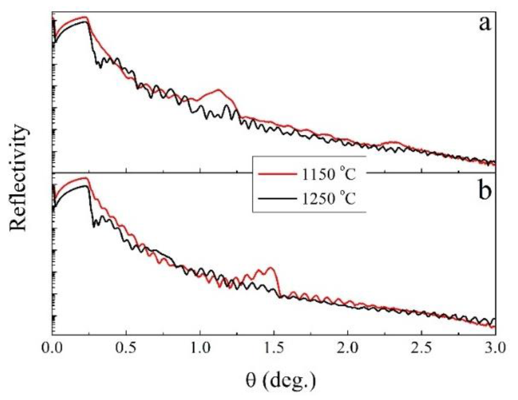
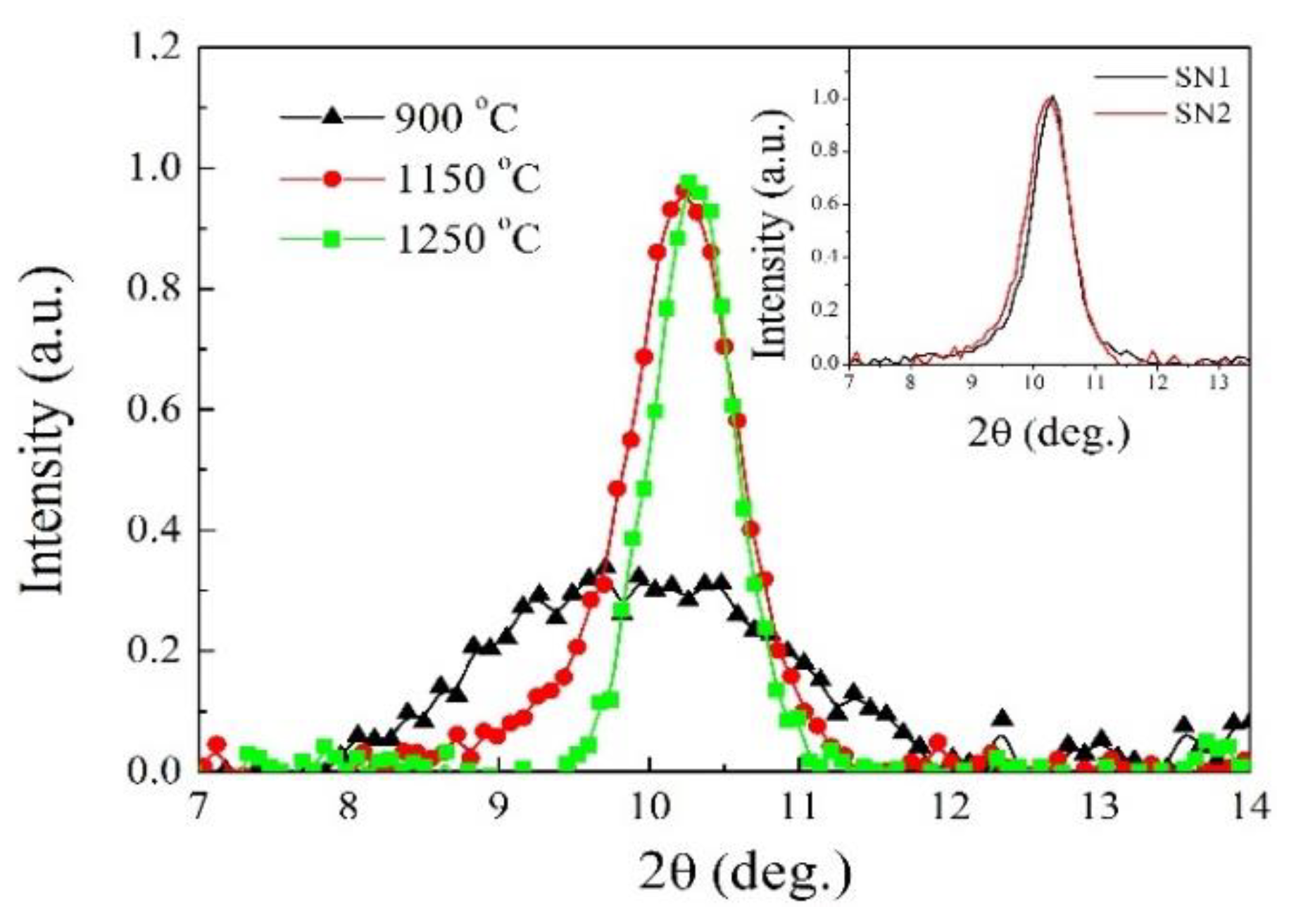
3.2. X-ray Studies
3.3. Photoluminescence Measurements
4. Conclusions
Author Contributions
Funding
Acknowledgments
Conflicts of Interest
References
- Kovalev, D.; Heckler, H.; Polisski, G.; Koch, F. Optical Properties of Si Nanocrystals. Phys. Status Solidi B 1999, 215, 871–932. [Google Scholar] [CrossRef]
- Takeoka, S.; Fujii, M.; Hayashi, S. Size-dependent photoluminescence from surface-oxidized Si nanocrystals in a weak confinement regime. Phys. Rev. B 2000, 62, 16820–16825. [Google Scholar] [CrossRef]
- Linnros, J.; Lalic, N.; Galeckas, A.; Grivickas, V. Analysis of the stretched exponential photoluminescence decay from nanometer-sized silicon crystals in SiO2. J. Appl. Phys. 1999, 86, 6128–6134. [Google Scholar] [CrossRef]
- Conibeer, G.; Green, M.; Cho, E.-C.; König, D.; Cho, Y.-H.; Fangsuwannarak, T.; Scardera, G.; Pink, E.; Huang, Y.; Puzzer, T.; et al. Silicon quantum dot nanostructures for tandem photovoltaic cells. Thin Solid Films 2008, 516, 6748–6756. [Google Scholar] [CrossRef]
- Wan, Z.; Huang, S.; Green, M.; Conibeer, G. Residual stress study of silicon quantum dot in silicon carbide matrix by Raman measurement. Phys. Status Solidi C 2011, 8, 185–188. [Google Scholar] [CrossRef]
- Zelenina, A.; Sarikov, A.; Gutsch, S.; Zakharov, N.; Werner, P.; Reichert, A.; Weiss, C.; Zacharias, M. Formation of size-controlled and luminescent Si nanocrystals from SiOxNy/Si3N4 hetero-superlattices. J. Appl. Phys. 2015, 117, 175303. [Google Scholar] [CrossRef]
- Heitmann, J.; Kovalev, D.; Schmidt, M.; Yi, L.X.; Scholz, R.; Eichhorn, F.; Zacharias, M. Synthesis and size control of Si nanocrystals by SiO/SiO2 superlattices and Er doping. MRS Proc. 2002, 737, F1.6. [Google Scholar] [CrossRef]
- Volodin, V.A.; Arzhannikova, S.A.; Gismatulin, A.A.; Kamaev, G.N.; Antonenko, A.K.; Cherkova, S.G.; Cherkov, A.G.; Kochubei, S.A.; Popov, A.A.; Robert, S.; et al. Laser pulse crystallization and optical properties of Si/SiO2 and Si/Si3N4 multilayer nano-heterostructures. Proc. SPIE 2012, 8700, 870008. [Google Scholar] [CrossRef]
- So, Y.-H.; Huang, S.; Conibeer, G.; Green, M.A. Formation and photoluminescence of Si nanocrystals in controlled multilayer structure comprising of Si-rich nitride and ultrathin silicon nitride barrier layers. Thin Solid Films 2011, 519, 5408–5412. [Google Scholar] [CrossRef]
- Chen, X.; Yang, W.; Yang, P.; Yuan, J.; Zhao, F.; Hao, J.; Tang, Y. Size-controlled Si quantum dots embedded in B-doped SiNx/Si3N4 superlatice for Si quantum dot solar cells. J. Mater. Sci. Mater. Electron. 2017, 28, 1322–1327. [Google Scholar] [CrossRef]
- Zhigunov, D.M.; Sarikov, A.; Chesnokov, Y.M.; Vasiliev, A.L.; Zakharov, N.; Kashkarov, P.K. Thickness and temperature depending intermixing of SiOx/SiO2 and SiOxNy/SiO2 superlattices: Experimental observation and thermodynamic modeling. Appl. Phys. Lett. 2016, 108, 223102. [Google Scholar] [CrossRef]
- Zelenina, A.; Sarikov, A.; Zhigunov, D.M.; Weiss, C.; Zakharov, N.; Werner, P.; López-Conesa, L.; Estradé, S.; Peiró, F.; Dyakov, S.A.; et al. Silicon nanocrystals in SiNx/SiO2 hetero-superlattices: The loss of size control after thermal annealing. J. Appl. Phys. 2014, 115, 244304. [Google Scholar] [CrossRef]
- Sain, B.; Das, D. Tunable photoluminescence from nc-Si/a-SiNx:H quantum dot thin films prepared by ICP-CVD. Phys. Chem. Chem. Phys. 2013, 15, 3881–3888. [Google Scholar] [CrossRef] [PubMed]
- Lin, C.-H.; Uen, W.-Y.; Lan, S.-M.; Huang, Y.-C.; Liao, S.-M.; Li, Z.-Y.; Yang, T.-N.; Ku, C.-T.; Chen, M.-C.; Huang, Y.-H. Luminescence mechanisms of silicon-rich nitride films fabricated by atmospheric pressure chemical vapor deposition in N2 and H2 atmospheres. J. Appl. Phys. 2009, 105, 053107. [Google Scholar] [CrossRef]
- Wang, M.; Li, D.; Yuan, Z.; Yang, D.; Que, D. Photoluminescence of Si-rich silicon nitride: Defect-related states and silicon nanoclusters. Appl. Phys. Lett. 2007, 90, 131903. [Google Scholar] [CrossRef]
- Delachat, F.; Carrada, M.; Ferblantier, G.; Grob, J.-J.; Slaoui, A. Properties of silicon nanoparticles embedded in SiNx deposited by microwave-PECVD. Nanotechnology 2009, 20, 415608. [Google Scholar] [CrossRef] [PubMed]
- Kistner, J.; Chen, X.; Weng, Y.; Strunk, H.P.; Schubert, M.B.; Werner, J.H. Photoluminescence from silicon nitride—No quantum effect. J. Appl. Phys. 2011, 110, 023520. [Google Scholar] [CrossRef]
- Giorgis, F.; Vinegoni, C.; Pavesi, L. Optical absorption and photoluminescence properties of a-Si1−xNx:H films deposited by plasma-enhanced CVD. Phys. Rev. B 2000, 61, 4693–4698. [Google Scholar] [CrossRef]
- Korchagina, T.T.; Marin, D.V.; Volodin, V.A.; Popov, A.A.; Vergnat, M. Structure and optical properties of SiNx:H films with Si nanoclusters produced by low-frequency plasma-enhanced chemical vapor deposition. Semiconductors 2009, 43, 1514–1520. [Google Scholar] [CrossRef]
- Molinari, M.; Rinnert, H.; Vergnat, M. Evolution with the annealing treatments of the photoluminescence mechanisms in a-SiNx: H alloys prepared by reactive evaporation. J. Appl. Phys. 2007, 101, 123532. [Google Scholar] [CrossRef]
- Liao, W.; Zeng, X.; Wen, X.; Chen, X.; Wang, W. Annealing and excitation dependent photoluminescence of silicon rich silicon nitride films with silicon quantum dots. Vacuum 2015, 121, 147–151. [Google Scholar] [CrossRef]
- Sarikov, A.; Zhigunov, D. Thermodynamic mechanism of the intermixing of multilayered structures in the SiOx/SiO2 superlattices with nanometer thick layers. Mater. Today Commun. 2017, 13, 163–169. [Google Scholar] [CrossRef]
- Zhigunov, D.M.; Martyshov, M.N.; Forsh, P.A.; Kamenskikh, I.A.; Yakunin, S.N.; Kashkarov, P.K. Structure-related current transport and photoluminescence in SiOxNy and SiNx based superlattices with Si nanocrystals. Phys. Status Solidi A Appl. Mater. 2017, 214, 1700040. [Google Scholar] [CrossRef]
- Hartel, A. Structural and Optical Properties of PECVD Grown Silicon Nanocrystals Embedded in SiOxNy Matrix. Ph.D. Thesis, Albert-Ludwigs-Universität Freiburg im Breisgau, Freiburg, Germany, 5 August 2013. [Google Scholar]
- Zhigunov, D.M.; Kamenskikh, I.A.; Lebedev, A.M.; Chumakov, R.G.; Logachev, Y.A.; Yakunin, S.N.; Kashkarov, P.K. X-ray reflectivity and photoelectron spectroscopy of superlattices with silicon nanocrystals. JETP Lett. 2017, 106, 517–521. [Google Scholar] [CrossRef]
- Heitmann, J.; Müller, F.; Zacharias, M.; Gösele, U. Silicon nanocrystals: Size matters. Adv. Mater. 2005, 17, 795–803. [Google Scholar] [CrossRef]
- Zelenina, A.; Dyakov, S.A.; Hiller, D.; Gutsch, S.; Trouillet, V.; Bruns, M.; Mirabella, S.; Löper, P.; López-Conesa, L.; López-Vidrier, J.; et al. Structural and optical properties of size controlled Si nanocrystals in Si3N4 matrix: The nature of photoluminescence peak shift. J. Appl. Phys. 2013, 114, 184311. [Google Scholar] [CrossRef]
- Timoshenko, V.Y.; Lisachenko, M.G.; Shalygina, O.A.; Kamenev, B.V.; Zhigunov, D.M.; Teterukov, S.A.; Kashkarov, P.K.; Heitmann, J.; Schmidt, M.; Zacharias, M. Comparative study of photoluminescence of undoped and erbium-doped size-controlled nanocrystalline Si/SiO2 multilayered structures. J. Appl. Phys. 2004, 96, 2254–2260. [Google Scholar] [CrossRef]


© 2019 by the authors. Licensee MDPI, Basel, Switzerland. This article is an open access article distributed under the terms and conditions of the Creative Commons Attribution (CC BY) license (http://creativecommons.org/licenses/by/4.0/).
Share and Cite
Zhigunov, D.M.; Popov, A.A.; Chesnokov, Y.M.; Vasiliev, A.L.; Lebedev, A.M.; Subbotin, I.A.; Yakunin, S.N.; Shalygina, O.A.; Kamenskikh, I.A. Near-IR Emitting Si Nanocrystals Fabricated by Thermal Annealing of SiNx/Si3N4 Multilayers. Appl. Sci. 2019, 9, 4725. https://doi.org/10.3390/app9224725
Zhigunov DM, Popov AA, Chesnokov YM, Vasiliev AL, Lebedev AM, Subbotin IA, Yakunin SN, Shalygina OA, Kamenskikh IA. Near-IR Emitting Si Nanocrystals Fabricated by Thermal Annealing of SiNx/Si3N4 Multilayers. Applied Sciences. 2019; 9(22):4725. https://doi.org/10.3390/app9224725
Chicago/Turabian StyleZhigunov, D. M., A. A. Popov, Yu. M. Chesnokov, A. L. Vasiliev, A. M. Lebedev, I. A. Subbotin, S. N. Yakunin, O. A. Shalygina, and I. A. Kamenskikh. 2019. "Near-IR Emitting Si Nanocrystals Fabricated by Thermal Annealing of SiNx/Si3N4 Multilayers" Applied Sciences 9, no. 22: 4725. https://doi.org/10.3390/app9224725